Metalenzele grafene ultra-late și plate au mai multe proprietăți(Ultrathin and flat graphene metalenses gain more properties)

Metasuprafețele sunt materiale noi 2D care pot controla în mod eficient componentele electrice și magnetice ale luminii (și alte unde electromagnetice) și le îndoiesc în direcții personalizate. Controlul direcției fasciculului poate aduce fenomene interesante; cea mai incredibilă fiind „efectul invizibilității mantalei”, unde undele de lumină ocolește un obiect care recreează imaginea dincolo de obiect, deoarece apa care curge într-un râu ar ocoli o piatră.Metalenzele au fost proiectate pentru un tip de undă electromagnetică, care se încadrează între radiația infraroșie și radiația cu microunde, numită radiație terahertz. Acest tip de radiații poate trece prin anumite materiale (cum ar fi țesăturile și materialele plastice), dar la o adâncime mai mică decât radiațiile cu microunde, din acest motiv este folosit pentru supravegherea și screening-ul de securitate.

Posted: Nov 27, 2017

Ultrathin and flat graphene metalenses gain more properties

(Nanowerk News) On the quest for miniaturization, scientists at the Center for Integrated Nanostructure Physics, within the Institute for Basic Science (IBS, South Korea), in collaboration with researchers from the University of Birmingham and the Korea Advanced Institute of Science and Technology (KAIST), develop credit card-thick, flat lenses with tunable features. These optical devices, made of graphene and a punctured gold surface, could become optical components for advanced applications, such as amplitude tunable lenses, lasers (i.e. vortex phase plates), and dynamic holography.

Comparison between conventional lenses and metalenses for terahertz (THz) radiation
Comparison between conventional lenses and metalenses for terahertz (THz) radiation. Metalenses are ultrathin (around 25 micrometers in thickness) and also very flat compared with conventional ones.
Metasurfaces are new 2D materials that can effectively control the electric and magnetic components of light (and other electromagnetic waves) and bend them to bespoken directions. Controlling the beam’s direction can bring out interesting phenomena; the most incredible being the “invisibility cloak effect”, where light waves bypass an object recreating the image beyond the object, as flowing water in a river would bypass a stone.
Published in Advanced Optical Materials („Amplitude Modulation of Anomalous Refractive Terahertz Waves with Gated-Graphene Metasurfaces”), the study presents the properties of a metasurface which works as a convex lens. Specifically, it is made of a gold sheet pierced with micrometer-sized U-shaped holes and covered with graphene. As the shape of common convex lenses allows light to be concentrated on a spot (or focus), think about a magnifying glass which can concentrate a light beam and even start a fire, so the particular pattern of the tiny apertures of the metalenses works by focusing the incoming beam.
graphene metalens features
Metalenses’ features. a) The metalenses are made with an atom-thick graphene sheet and a gold thin surface with tiny U-shaped holes. b) The device can convert the circular polarization of the erahertz wave from left to right. Moreover, by rotating the holes’ pattern, the beam (or wave) can be bent it to the desired angle.
In addition, these microholes can also change light polarization. While natural light is generally unpolarized before being reflected, the team used circularly polarized waves, that is a light beam where the direction of the electric field is corkscrew spiraling. This metalens can convert the left-circular polarization wave (going counterclockwise if seen straight in front) to right-circular polarization (clockwise). The researchers managed to obtain a conversion rate of 35%. Converting circular polarization could be useful in a number of fields, for example biosensing and telecommunications.
In order to control even more properties, the scientists took advantage of graphene’s unique electronic features and used them to tune the output beam’s intensity or amplitude. Here graphene plays the role of the exposure of a camera. In the case of the camera, a mechanical control allows a certain shutter’s opening time and size to determine the amount of light entering the instrument. These metalenses instead, regulate the exposure via an electric tension applied to the graphene sheet, without the need for bulky components. When voltage is applied to the graphene layer, the output beam becomes weaker. “Using metalenses, you can make microscopes, cameras, and tools used in very sensitive optical measurements, much more compact,” clarifies Teun-Teun Kim, the first author of the study.
The function of the U-shaped pattern and graphene is to concentrate the beam’s direction and modulate signal intensity
The function of the U-shaped pattern and graphene is to concentrate the beam’s direction and modulate signal intensity. Different U-shaped hole pattern on the metasurface create a striped (a) and a focalized (b) beam output. In b) the beam is concentrated to a small area (red spot), in the same way as a magnifying glass focuses light on a specific point. Moreover, by applying a gated voltage (2.2 V) on graphene, the output beam intensity becomes weaker. Graphene function could be compared to the exposure of a camera.
The metalenses were designed for a type of electromagnetic wave, which falls in-between infrared radiation and microwave radiation, called terahertz radiation. This type of radiation can pass through some materials (like fabrics and plastics), but at a shorter depth than microwave radiation, for this reason it is employed for surveillance and security screening.
“While conventional optical lenses have a thickness of several centimeters to several millimeters, this metalens is just a few tens of micrometers thick. The intensity of the focused light can be effectively controlled and it could find useful applications in ultra-small optical instruments,” highlights the scientists.Teun-Teun Kim, the first author of the study.
Source: Institute for Basic Science

Cerneluri cu semiconductoare ecologice, care utilizează surfactanți(Eco-friendly waterborne semiconductor inks using surfactant)

a dezvoltat o tehnologie pentru a produce cerneluri semiconductoare pe bază de apă ecologice folosind surfactant, aditivi care amestecă substanțe de diferite proprietăți și componentă a săpunului.
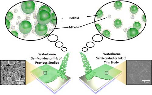
Semiconductorii polimeri sunt compuși ai carbonului care prezintă proprietățile electrice ale semiconductorilor. Acesta a fost evidențiat ca un material de generație următoare de dispozitive inteligente pentru uzură etc., nu numai pentru că sunt flexibile și ușoare în greutate, dar pot fi prelucrate într-o zonă extinsă și cu un cost redus prin procesul de soluționare. Cu toate acestea, există o problemă care cauzează o poluare semnificativă a mediului, deoarece solvenții organici toxici sunt utilizați în acest proces;a produs cerneluri semiconductoare cu apă; cerneala semiconductoare pe bază de apă recent dezvoltată are particule coloidale mici și miceluri surfactante comparativ la cernelurile semiconductoare pe bază de apă în studiile anterioare.

Posted: Nov 27, 2017

Eco-friendly waterborne semiconductor inks using surfactant

(Nanowerk News) A research team of Energy Science and Engineering at Daegu Gyeongbuk Institute of Science and Technology (DGIST) has developed a technology to produce environmentally friendly water-borne semiconductor inks using surfactant, which is additives that mix substances of different properties and a component of soap.

Polymer semiconductors are carbon compounds showing the electrical properties of semiconductors. It has been highlighted as a next-generation material of wearable smart devices, etc. not only because they are flexible and light in weight, but also they can be processed in a wide area a low cost through the solution process. However, there is an issue that it causes significant environmental pollution as toxic organic solvents are used in the process.
Despite the limitations, the research team has developed a semiconductor surface control technique using surfactants for environmentally friendly semiconductor manufacturing processes that do not use toxic organic solvents and has produced water-borne semiconductor inks.
a comparison of waterborne semiconductor inks
A comparison of the waterborne semiconductor ink of this study and that of the previous studies. (Image: DGIST)
In the study (Energy & Environmental Science, „Universal selection rule for surfactants used in miniemulsion processes for eco-friendly and high performance polymer semiconductors”), the newly developed waterborne semiconductor ink of the research team has small colloidal particles and less surfactant micelles compared to the waterborne semiconductor inks in the previous studies. As a result, it has a relatively flat surface than the conventional waterborne semiconductor inks. The black and white image in the figure shows the comparison of the surface of the thin film made with the waterborne semiconductor ink developed in this study and conventional one.
According to the research team, the technique is expected to be applied in various electronic devices such as P-type and N-type transistors as well as PN diodes, complementary inverters, photodiodes as high-quality thin films.
Professor Chung stressed the significance of the study by stating „This research has fundamentally solved the environmental pollution problem generated during the production of organic semiconductor, which is spotlighted as the core material of wearable electronic devices. We have developed a source technology that can disperse various semiconductor materials into water through the simple chemical modification. We expect that it can be used in various optoelectronic devices ranging from transistors to solar cell, composite circuit, and image sensor.”
Source: Daegu Gyeongbuk Institute of Science and Technology (DGIST)

Senzori bazați pe plante pentru colectarea inteligenței(Plant-Based Sensors to Collect Intelligence)

DARPA evaluează faptul că senzorii de inteligență tradiționali ai armatei nu sunt întotdeauna optimi pentru sarcinile care au devenit din ce în ce mai complexe și provocatoare.Plantele sunt foarte atinse de mediile lor și manifestă în mod natural răspunsuri fiziologice la stimuli de bază cum ar fi lumina și temperatura, dar, de asemenea, în unele cazuri la atingere, chimicale, dăunători și agenți patogeni

Plant

Descoperirea celulelor solare deschide o nouă fereastră pentru alimentarea orașelor de mâine(Solar cell discovery opens a new window to powering tomorrow’s cities)

au determinat structura moleculara a electrozilor de lucru cu celule solare in cadrul unui dispozitiv complet asamblat care functioneaza ca o fereastra. Constatarea, publicată în Nanoscale , ajută la avansarea unei tehnologii inteligente de ferestre care ar putea permite orașelor să se apropie de obiectivul de a fi durabile din punct de vedere energetic.
Experimentele au fost efectuate pe celulele solare sensibile la coloranți, care sunt transparente și astfel foarte potrivite pentru utilizarea în sticlă. Încercările de a crea tehnologii inteligente pentru ferestre au fost limitate de numeroase mecanisme moleculare necunoscute între electrozii și electrolitul care se combină pentru a determina modul în care funcționează dispozitivul. a aratat ca anumite ingrediente chimice, unele dintre care pana acum au fost trecute cu vederea, pot influenta in mod clar performanta fotovoltaice a acestor celule solare, Cole a spus.

Posted: Nov 23, 2017

Solar cell discovery opens a new window to powering tomorrow’s cities

(Nanowerk News) Buildings of the future may come equipped with windows that can generate their own electricity, thanks to a finding of a team led by Jacqui Cole, a materials scientist from the University of Cambridge, UK, currently based at the U.S. Department of Energy’s (DOE) Argonne National Laboratory.

For the first time, Cole and colleagues determined the molecular structure of working solar cell electrodes within a fully assembled device that works like a window. The finding, published in Nanoscale, helps advance smart window technology that could enable cities to move closer to the goal of being energy sustainable.
The experiments were performed on dye-sensitized solar cells, which are transparent and thus well-suited for use in glass. Attempts to create smart window technologies have been limited by the many unknown molecular mechanisms between the electrodes and electrolyte that combine to determine how the device operates.
“Most previous studies have modeled the molecular function of these working electrodes without considering the electrolyte ingredients,” Cole said. “Our work shows that these chemical ingredients can clearly influence the performance of solar cells, so we can now use this knowledge to tune the ions to increase photovoltaic efficiency.”
To make the discovery, Cole — the 1851 Royal Commission 2014 Design Fellow — and her colleagues used neutron reflectometry to probe the function and interplay of the electrolyte ingredients with electrodes of the dye-sensitized solar cells. Neutron reflectometry, similar to X-ray reflectometry techniques, allows scientists to measure the structure of thin films with high resolution. But it was the fact that the tests were performed in a window-like system that made for a significant discovery.
“Prior research considered the working electrodes outside the device, so there has been no path to determine how the different device components interact,” Cole said. “Our work signifies a huge leap forward as it’s the world’s first example of applying in situ neutron reflectometry to dye-sensitized solar cells.”
Previous efforts to characterize the dye/titanium dioxide interface in these solar cells have been limited to determining this interfacial structure within an environment exposed to air or in a solvent medium. Because of these constraints, these solar cell environments are essentially artificial with limited relevance for window applications.
With this discovery, however, Cole and colleagues have moved beyond artificial constraints. In doing so, they can better understand how a thin-film electrode containing titanium dioxide, a naturally occurring compound found in paint, sunscreen and food coloring, can have a huge impact on solar cell efficiency.
“Our work has shown that certain chemical ingredients, some of which have so far been overlooked, can clearly influence the photovoltaic performance of these solar cells,” Cole said.
More efficient solar cells like these can move smart window technology closer to the marketplace, said Cole, adding that the science is almost there.
“We just need a modest boost in performance to make these solar cells competitive,” Cole said, “since price-to-performance governs the economics of the solar cell industry. And manufacturing dye-sensitized solar cells is very cheap relative to other solar cell technologies.”
Performance-wise, the cells recently broke a world record with a power conversion efficiency of 14.3 percent using a dye-sensitized electrode featuring two co-sensitized metal-free organic dyes. These dyes “promise cheaper, more environmentally friendly synthetic routes and greater molecular design flexibility than their metal-containing counterparts,” according to the paper.
Source: By Ron Walli, Argonne National Laboratory

Descoperirea celulelor solare deschide o nouă fereastră pentru alimentarea orașelor de mâine(

au determinat structura moleculara a electrozilor de lucru cu celule solare in cadrul unui dispozitiv complet asamblat care functioneaza ca o fereastra.ei pot intelege mai bine cum un electrod subtire care contine dioxid de titan, un compus natural care se gaseste in vopsea, protectie solara si colorarea alimentelor, poate avea un impact imens asupra eficientei celulelor solare.

Posted: Nov 23, 2017

Solar cell discovery opens a new window to powering tomorrow’s cities

(Nanowerk News) Buildings of the future may come equipped with windows that can generate their own electricity, thanks to a finding of a team led by Jacqui Cole, a materials scientist from the University of Cambridge, UK, currently based at the U.S. Department of Energy’s (DOE) Argonne National Laboratory.

For the first time, Cole and colleagues determined the molecular structure of working solar cell electrodes within a fully assembled device that works like a window. The finding, published in Nanoscale, helps advance smart window technology that could enable cities to move closer to the goal of being energy sustainable.
The experiments were performed on dye-sensitized solar cells, which are transparent and thus well-suited for use in glass. Attempts to create smart window technologies have been limited by the many unknown molecular mechanisms between the electrodes and electrolyte that combine to determine how the device operates.
“Most previous studies have modeled the molecular function of these working electrodes without considering the electrolyte ingredients,” Cole said. “Our work shows that these chemical ingredients can clearly influence the performance of solar cells, so we can now use this knowledge to tune the ions to increase photovoltaic efficiency.”
To make the discovery, Cole — the 1851 Royal Commission 2014 Design Fellow — and her colleagues used neutron reflectometry to probe the function and interplay of the electrolyte ingredients with electrodes of the dye-sensitized solar cells. Neutron reflectometry, similar to X-ray reflectometry techniques, allows scientists to measure the structure of thin films with high resolution. But it was the fact that the tests were performed in a window-like system that made for a significant discovery.
“Prior research considered the working electrodes outside the device, so there has been no path to determine how the different device components interact,” Cole said. “Our work signifies a huge leap forward as it’s the world’s first example of applying in situ neutron reflectometry to dye-sensitized solar cells.”
Previous efforts to characterize the dye/titanium dioxide interface in these solar cells have been limited to determining this interfacial structure within an environment exposed to air or in a solvent medium. Because of these constraints, these solar cell environments are essentially artificial with limited relevance for window applications.
With this discovery, however, Cole and colleagues have moved beyond artificial constraints. In doing so, they can better understand how a thin-film electrode containing titanium dioxide, a naturally occurring compound found in paint, sunscreen and food coloring, can have a huge impact on solar cell efficiency.
“Our work has shown that certain chemical ingredients, some of which have so far been overlooked, can clearly influence the photovoltaic performance of these solar cells,” Cole said.
More efficient solar cells like these can move smart window technology closer to the marketplace, said Cole, adding that the science is almost there.
“We just need a modest boost in performance to make these solar cells competitive,” Cole said, “since price-to-performance governs the economics of the solar cell industry. And manufacturing dye-sensitized solar cells is very cheap relative to other solar cell technologies.”
Performance-wise, the cells recently broke a world record with a power conversion efficiency of 14.3 percent using a dye-sensitized electrode featuring two co-sensitized metal-free organic dyes. These dyes “promise cheaper, more environmentally friendly synthetic routes and greater molecular design flexibility than their metal-containing counterparts,” according to the paper.
Source: By Ron Walli, Argonne National Laboratory

Îmbunătățirea capacităților de detectare cuantică a diamantului(Enhancing the quantum sensing capabilities of diamond)

senzori si resurse imbunatatite pentru tehnologiile cuantice.
Diamantele sunt fabricate din atomi de carbon într-o structură cristalină, dar dacă un atom de carbon este înlocuit cu un alt tip de atom, acest lucru va duce la un defect de zăbrele. Un astfel de defect este Nitrogen-Vacancy (NV), unde un atom de carbon este înlocuit cu un atom de azot, iar vecinul său lipsește (un spațiu gol rămâne în locul său).
Dacă acest defect este iluminat cu un laser verde, în urma răspunsului acesta va emite lumină roșie (fluorescentă) cu o caracteristică interesantă: intensitatea sa variază în funcție de proprietățile magnetice din mediul înconjurător. Această caracteristică unică face ca centrul NV să fie deosebit de util pentru măsurarea câmpurilor magnetice, a imaginilor magnetice (MRI), a calculului cuantic și a informațiilor.

Posted: Nov 22, 2017

Enhancing the quantum sensing capabilities of diamond

(Nanowerk News) Researchers have discovered that dense ensembles of quantum spins can be created in diamond with high resolution using an electron microscopes, paving the way for enhanced sensors and resources for quantum technologies.

Diamonds are made of carbon atoms in a crystalline structure, but if a carbon atom is replaced with another type of atom, this will result in a lattice defect. One such defect is the Nitrogen-Vacancy (NV), where one carbon atom is replaced by a nitrogen atom, and its neighbor is missing (an empty space remains in its place).
If this defect is illuminated with a green laser, in response it will emit red light (fluoresce) with an interesting feature: its intensity varies depending on the magnetic properties in the environment. This unique feature makes the NV center particularly useful for measuring magnetic fields, magnetic imaging (MRI), and quantum computing and information.
In order to produce optimal magnetic detectors, the density of these defects should be increased without increasing environmental noise and damaging the diamond properties.
Now, scientists from the research group of Nir Bar-Gill at the Hebrew University of Jerusalem’s Racah Institute of Physics and Department of Applied Physics, in cooperation with Prof. Eyal Buks of the Technion – Israel Institute of Technology, have shown that ultra-high densities of NV centers can be obtained by a simple process of using electron beams to kick carbon atoms out of the lattice.
Diamond Sample Illuminated by Green Light
This photo shows a diamond sample illuminated by green light in home-built microscope. The sample is placed on a special mount, within a printed circuit board, used to deliver microwaves which allow quantum manipulations and magnetic sensing with the NVs. (Image: Yoav Romach
This work, published in the scientific journal Applied Physics Letters („Enhanced concentrations of nitrogen-vacancy centers in diamond through TEM irradiation”), is a continuation of previous work in the field, and demonstrates an improvement in the densities of NV centers in a variety of diamond types. The irradiation is performed using an electron beam microscope (Transmission Electron Microscope or TEM), which has been specifically converted for this purpose. The availability of this device in nanotechnology centers in many universities in Israel and around the world enables this process with high spatial accuracy, quickly and simply.
The enhanced densities of the NV color centers obtained, while maintaining their unique quantum properties, foreshadow future improvements in the sensitivity of diamond magnetic measurements, as well as promising directions in the study of solid state physics and quantum information theory.
Nitrogen Vacancy (NV) color centers exhibit remarkable and unique properties, including long coherence times at room temperature (~ ms), optical initialization and readout, and coherent microwave control.
„This work is an important stepping stone toward utilizing NV centers in diamond as resources for quantum technologies, such as enhanced sensing, quantum simulation and potentially quantum information processing”, said Bar-Gill, an Assistant Professor in the Dept. of Applied Physics and Racah Institute of Physics at the Hebrew University, where he founded the Quantum Information, Simulation and Sensing lab.
„What is special about our approach is that it’s very simple and straightforward,” said Hebrew University researcher Dima Farfurnik. „You get sufficiently high NV concentrations that are appropriate for many applications with a simple procedure that can be done in-house.”
Source: The Hebrew University of Jerusalem

Comunicarea la viteza luminii cu grafen(Communicating at the speed of light with graphene)

mesaje cu viteza luminii.
Materialele subțiri din două dimensiuni, realizate prin strat atomic de strat atomic, pot permite comunicații la o viteză mai mare și consumuri de energie mai mici decât cele realizate anterior.Acestea ar putea fi baza sistemelor optice de interconectare de generație viitoare în infrastructurile Air Force, a spus ea.

Posted: Nov 22, 2017

Communicating at the speed of light with graphene

(Nanowerk News) Imagine how much we could accomplish in a day if we could exchange messages at the speed of light.

Thin two-dimensional materials, made atomic layer by atomic layer, may enable communications at higher speed and lower power consumptions than previously realized. Multidisciplinary research in this field is happening now at the University of Delaware.
Tingyi Gu, assistant professor of electrical and computer engineering at the University of Delaware
Tingyi Gu, assistant professor of electrical and computer engineering at the University of Delaware.
For this work, Tingyi Gu, an assistant professor in the Department of Electrical and Computer Engineering, is one of 43 scientists nationwide to receive a grant this year through the Air Force Office of Scientific Research (AFOSR) Young Investigator Program this year.

The AFOSR Young Investigator Program was established to foster creative basic research. It is awarded to scholars with exceptional ability and promise who have earned their doctoral degrees within the last five years.

Under this three-year, $450,000 grant, Gu is developing „next-generation hybrid optical communications”–small, lightweight devices for efficient light generation and transportation, enabling high speed and low power optical interconnects, which is an interface between electronic signals in computers and optical fiber communication signals.

In optical communications, signals are transmitted via light. Fiber communication is the backbone bundling all the signals.
In contrast, the communications devices you use everyday, like laptops and phones, use wireless radio signals to transmit signals.
To build devices for optical communications, Gu first uses software to design the devices, optimizing their optical, electronic and thermal properties. Then, she will work with the team at the UD Nanofabrication Facility to make the devices.
„The UD Nanofabrication Facility team is actively working with Prof. Gu’s group on this project and we have recently made promising progress on fabricating those high quality nanophotonic devices on a large scale,” said Iulian Codreanu, Ph.D., director of operations at UD NanoFab.
The devices start with silicon, a material commonly used in photonics–the study of light and its applications. Then graphene, a two-dimensional material made from a single layer of atoms, is bonded onto silicon chips. Graphene can improve chip performance, including generation, amplification, modulation, and detection of optical signals.
„Its unique structure gives it unique electronic properties not enabled by bulk materials,” said Gu.
In 2010, the pioneers of graphene research, located at the University of Manchester, won the Nobel Prize in Physics. Since then, „two-dimensional materials have been a hot area of research,” said Gu.
Gu isn’t just making devices–she is testing them in order to improve speed, performance, and scalability of devices made with these materials. These could be the basis of next-generation optical interconnect systems in Air Force infrastructures, she said.
„Together we are doing very sharp engineering in combination with hot science,” said Gu. „This grant gives me more opportunity to tap the potential of my research.”
Gu’s students will also benefit from this award.
„This is a wonderful opportunity for students to get trained to understand the process from beginning to end,” she said, „which is critical for their future careers.”
Gu’s work with photonic devices has also garnered attention from NASA, which granted her an Early Career Faculty Award earlier this year.
Dennis Prather, Engineering Alumni Professor in the Department of Electrical and Computer Engineering and Dr. Gu’s faculty mentor, has been studying silicon photonics for nearly two decades. He is impressed by Gu’s success thus far.
„I’m certain she will be a future pillar of our department and I’m already so proud to call her my colleague,” he said.
Source: By Julie Stewart, University of Delaware

Izolatori topologici: este suficientă o singură privire(Topological insulators: one glimpse is enough)

Izolatorii topologici sunt materiale noi cu proprietăți electronice speciale și au un interes fundamental și orientat spre aplicații.Izolatoarele topologice sunt lucruri ciudate. Cea mai mare parte a unui astfel de cristal este izolator și nu poate purta un curent electric, totuși suprafețele aceluiași cristal conduc. Aceste materiale noi au un interes fundamental deosebit, dar sunt, de asemenea, foarte promițătoare pentru o serie de aplicații viitoare în tipuri speciale de electronică și în calculul cuantic și astfel fac obiectul unui efort substanțial de cercetare fizică. Semnificația materialelor topologice a fost subliniată anul trecut prin acordarea Premiului Nobel pentru dezvoltarea teoriilor fundamentale care stabilesc existența și comportamentul materiei topologice.

Posted: Nov 21, 2017

Topological insulators: one glimpse is enough

(Nanowerk News) The Nobel Prize for physics in 2016 was awarded for the theory of topological matter. Topological insulators are new materials with special electronic properties and are of great fundamental and applications-oriented interest. Nevertheless, physicists have wrestled with a ten-year-old puzzle in which the results from the two best methods to probe their electronic states disagree. Researchers from Amsterdam, including two FOM-funded PhD candidates, with collaborators in France, Switzerland and Germany now know exactly why.

he band structure of a topological insulator measured using photoemission
The band structure of a topological insulator measured using photoemission. The dark areas indicate which energies [on the y-axis] go together with which (here inverse) wavelengths [on the x-axis] for the electron waves in the solid. After 20 seconds exposure to the UV light involved in doing a photoemission experiment (right-hand image) the band structure is very different to that after only 1 second exposure (left-hand image). The coloured circles show the position of the Dirac point. (Image: Universiteit van Amsterdam)
Topological insulators are strange stuff. The bulk of such a crystal is insulating and cannot carry an electrical current, yet the surfaces of that same crystal are conducting. These new materials are of great fundamental interest but are also very promising for a number of future applications in special types of electronics and in quantum computation, and so they are the subject of a substantial physics research effort. The significance of topological materials was underlined last year with the award of the Nobel Prize for the development of fundamental theories setting out the existence and behaviour of topological matter.
There are two powerful experimental methods to examine the behaviour of the electrons – the particles that carry electrical current – at the surface of a topological insulator. The first involves sending a current through the system in the presence of a very large magnetic field, and is known as magnetotransport. The second involves the use of an ultraviolet light beam to examine the surface of the crystal. In this case, the energy of a light particle can be absorbed by an electron and in this way those near the surface can escape the crystal and be analysed. Researchers can harness this photo-electric effect to gather valuable information on the electronic properties at the surface of a topological insulator, the place where all the action is. This kind of experiment is called photoemission.
Since more than 10 years, researchers have been baffled as to why these two experiments completely disagree when applied to topological insulators. Now researchers from Amsterdam, including two FOM-funded PhD candidates, together with collaborators in France, Switzerland and Germany recently caught a glimpse of the reasons why. The hypothesis? The very first UV light flash, required to record the photoemission data, itself alters the electronic structure at the surface.
The quantity that describes and explains how electrons in a solid do their stuff is called the band structure. It can be seen as a sort of road network, that maps out the allowed combinations of energy and wavelength the electron-waves can have in the crystal. A slice through such a band structure can be easily displayed as a 2D image like those in the images shown here. This kind of snapshot contains valuable information on the electronic structure of a topological insulator, and in particular the energy location of the crossing-point of the two branches visible in the band structure. This special feature – highlighted with a coloured marker in the images – is called the Dirac point, named for theoretical physicist Paul Dirac whose theory first described electrons like those at the surface of a topological insulator.
Normally, recording a band structure image costs a minute or more. But here the researchers worked hard to bring this down to just a single second, and the left-hand image was the result. The Dirac point (green circle) comes at an energy matching that from magnetotransport data. After only 20 seconds of UV exposure, the red marker in right-hand picture shows that the Dirac point, and the rest of the band structure with it has slid way down in energy, far from the value found in the transport experiments.
It was already known that molecules that stick to the surface of the topological insulator can cause a downward shift of the Dirac point. These new experiments were able to disentangle the effect of the molecules at the surface and that of the UV light, so the researchers could demonstrate that the very first flash of light in fact plays the role of the starter’s pistol, triggering a rapid downward slide of the Dirac point.
These new results are very useful, as photoemission is a very important experiment in the field of topological materials. But do they mean that photoemission is ripe for the rubbish bin? On the contrary! Now that the effect of the UV light is properly understood, protocols could be developed as to how photoemission can be used in the right way in future studies of topological insulators. The photoemission results and the guidelines for improved experimental procedures were published this week in the leading (open access) physics journal, Physical Review X („Trigger of the ubiquitous surface band bending in 3D topological insulators”).
Source: Universiteit van Amsterdam

Proiectarea de aliaje noi de metal folosind nanostructuri construite(Designing new metal alloys using engineered nanostructures)

Un candidat primar pentru acest „material cu care se confruntă plasmă” este tungstenul, datorită punctului său de topire ridicat – cel mai mare dintre metale sub formă pură și randament scăzut de sputtering (numărul de atomi ejectați de ionii energetici din plasmă). Cu toate acestea, stabilitatea tungstenului împotriva recristalizării, rezistența la oxidare, toleranța la radiații pe termen lung și performanța mecanică sunt problematice.tudiază, de asemenea, comportamentul de deformare a „nanolaminatelor” metalice care constau din straturi cristaline și amorfe alternante și încearcă să abordeze limita teoretică a rezistenței aliajelor ușoare de aluminiu prin strategii sinergice de dopaj chimic (adăugând alte elemente într-un material pentru a-și schimba proprietățile).

Posted: Nov 21, 2017

Designing new metal alloys using engineered nanostructures

(Nanowerk News) Materials science is a field that Jason Trelewicz has been interested in since he was a young child, when his father—an engineer—would bring him to work. In the materials lab at his father’s workplace, Trelewicz would use optical microscopes to zoom in on material surfaces, intrigued by all the distinct features he would see as light interacted with different samples.

Jason Trelewicz
Materials scientist Jason Trelewicz in an electron microscopy laboratory at Brookhaven’s Center for Functional Nanomaterials, where he characterizes nanoscale structures in metals mixed with other elements.
Now, Trelewicz—an assistant professor in the College of Engineering and Applied Sciences’ Department of Materials Science and Chemical Engineering with a joint appointment in the Institute for Advanced Computational Science at Stony Brook University and principal investigator of the Engineered Metallic Nanostructures Laboratory—takes advantage of the much higher magnifications of electron microscopes to see tiny nanostructures in fine detail and learn what happens when they are exposed to heat, radiation, and mechanical forces.

In particular, Trelewicz is interested in nanostructured metal alloys (metals mixed with other elements) that incorporate nanometer-sized features into classical materials to enhance their performance. The information collected from electron microscopy studies helps him understand interactions between structural and chemical features at the nanoscale. This understanding can then be employed to tune the properties of materials for use in everything from aerospace and automotive components to consumer electronics and nuclear reactors.

Since 2012, when he arrived at Stony Brook University, Trelewicz has been using the electron microscopes and the high-performance computing (HPC) cluster at the Center for Functional Nanomaterials (CFN)—a U.S. Department of Energy (DOE) Office of Science User Facility at Brookhaven National Laboratory—to perform his research.

“At the time, I was looking for ways to apply my idea of stabilizing nanostructures in metals to an application-oriented problem,” said Trelewicz. “I’ve long been interested in nuclear energy technologies, initially reading about fusion in grade school. The idea of recreating the processes responsible for the energy we receive from the sun here on earth was captivating, and fueled my interest in nuclear energy throughout my entire academic career. Though we are still very far away from a fusion reactor that generates power, a large international team on a project under construction in France called ITER is working to demonstrate a prolonged fusion reaction at a large scale.”

Plasma-facing materials for fusion reactors

Nuclear fusion—the reaction in which atomic nuclei collide—could provide a nearly unlimited supply of safe, clean energy, like that naturally produced by the sun through fusing hydrogen nuclei into helium atoms. Harnessing this carbon-free energy in reactors requires generating and sustaining a plasma, an ionized gas, at the very high temperatures at which fusion occurs (about six times hotter than the sun’s core) while confining it using magnetic fields. Of the many challenges currently facing fusion reactor demonstrations, one of particular interest to Trelewicz is creating viable materials to build a reactor.
“The formidable materials challenges for fusion are where I saw an opportunity for my research—developing materials that can survive inside the fusion reactor, where the plasma will generate high heat fluxes, high thermal stresses, and high particle and neutron fluxes,” said Trelewicz. “The operational conditions in this environment are among the harshest in which one could expect a material to function.”
A primary candidate for such “plasma-facing material” is tungsten, because of its high melting point—the highest one among metals in pure form—and low sputtering yield (number of atoms ejected by energetic ions from the plasma). However, tungsten’s stability against recrystallization, oxidation resistance, long-term radiation tolerance, and mechanical performance are problematic.
Trelewicz thinks that designing tungsten alloys with precisely tailored nanostructures could be a way to overcome these problems. In August, he received a $750,000 five-year award from the DOE’s Early Career Research Program to develop stable nanocrystalline tungsten alloys that can withstand the demanding environment of a fusion reactor. His research is combining simulations that model atomic interactions and experiments involving real-time ion irradiation exposure and mechanical testing to understand the fundamental mechanisms responsible for the alloys’ thermal stability, radiation tolerance and mechanical performance. The insights from this research will inform the design of more resilient alloys for fusion applications.
atomistic simulations to explore the segregation of solute species to grain boundaries (GBs)—interfaces between grains—in nanostructured alloys
Trelewicz and his students perform large-scale atomistic simulations to explore the segregation of solute species to grain boundaries (GBs)—interfaces between grains—in nanostructured alloys, as shown here for an aluminum-magnesium (Al-Mg) system, and its implications for the governing deformation mechanisms. They are using the insights gained through these simulations to design lightweight alloys with theoretical strengths. (Image: Jason Trelewicz )
In addition to the computational resources they use at their home institution, Trelewicz and his lab group are using the HPC cluster at the CFN—and those at other DOE facilities, such as Titan at Oak Ridge Leadership Computing Facility (a DOE Office of Science User Facility at Oak Ridge National Laboratory)—to conduct large-scale atomistic simulations as part of the project.
“The length scales of the structures we want to design into our materials are on the order of a few nanometers to 100 nanometers, and a single simulation can involve up to 10 million atoms,” said Trelewicz. “Using HPC clusters, we can build a system atom-by-atom, representative of the structure we would like to explore experimentally, and run simulations to study the response of that system under various external stimuli. For example, we can fire a high-energy atom into the system and watch what happens to the material and how it evolves, hundreds or thousands of times. Once damage has accumulated in the structure, we can simulate thermal and mechanical forces to understand how defect structure impacts other behavior.”
These simulations inform the structures and chemistries of experimental alloys, which Trelewicz and his students fabricate at Stony Brook University through high-energy milling. To characterize the nanoscale structure and chemical distribution of the engineered alloys, they extensively use the microscopy facilities at the CFN—including scanning electron microscopes, transmission electron microscopes, and scanning transmission electron microscopes. Imaging is conducted at high resolution and often combined with heating within the microscope to examine in real time how the structures evolve with temperature. Experiments are also conducted at other DOE national labs, such as Sandia through collaboration with materials scientist Khalid Hattar of the Ion Beam Laboratory. Here, students in Trelewicz’s research group simultaneously irradiate the engineered alloys with an ion beam and image them with an electron microscope over the course of many days.
“Though this damage does not compare to what the material would experience in a reactor, it provides a starting point to evaluate whether or not the engineered material could indeed address some of the limitations of tungsten for fusion applications,” said Trelewicz.
Electron microscopy at the CFN has played a key role in an exciting discovery that Trelewicz’s students recently made: an unexpected metastable-to-stable phase transition in thin films of nanostructured tungsten. This phase transition drives an abnormal „grain” growth process in which some crystalline nanostructure features grow very dramatically at the expense of others. When the students added chromium and titanium to tungsten, this metastable phase was completely eliminated, in turn enhancing the thermal stability of the material.
“One of the great aspects of having both experimental and computational components to our research is that when we learn new things from our experiments, we can go back and tailor the simulations to more accurately reflect the actual materials,” said Trelewicz.

Other projects in Trelewicz’s research group

The research with tungsten is only one of many projects ongoing in the Engineered Metallic Nanostructures Laboratory.
“All of our projects fall under the umbrella of developing new metal alloys with enhanced and/or multifunctional properties,” said Trelewicz. “We are looking at different strategies to optimize material performance by collectively tailoring chemistry and microstructure in our materials. Much of the science lies in understanding the nanoscale mechanisms that govern the properties we measure at the macroscale.”
Through a National Science Foundation CAREER (Faculty Early Career Development Program) award, Trelewicz and his research group are exploring another class of high-strength alloys—amorphous metals, or “metallic glasses,” which are metals that have a disordered atomic structure akin to glass. Compared to everyday metals, metallic glasses are often inherently higher strength but usually very brittle, and it is difficult to make them in large parts such as bulk sheets. Trelewicz’s team is designing interfaces and engineering them into the metallic glasses—initially iron-based and later zirconium-based ones—to enhance the toughness of the materials, and exploring additive manufacturing processes to enable sheet-metal production. They will use the Nanofabrication Facility at the CFN to fabricate thin films of these interface-engineered metallic glasses for in situ analysis using electron microscopy techniques.
In a similar project, they are seeking to understand how introducing a crystalline phase into a zirconium-based amorphous alloy to form a metallic glass matrix composite (composed of both amorphous and crystalline phases) augments the deformation process relative to that of regular metallic glasses. Metallic glasses usually fail catastrophically because strain becomes localized into shear bands. Introducing crystalline regions in the metallic glasses could inhibit the process by which strain localizes in the material. They have already demonstrated that the presence of the crystalline phase fundamentally alters the mechanism through which the shear bands form.
Trelewicz and his group are also exploring the deformation behavior of metallic “nanolaminates” that consist of alternating crystalline and amorphous layers, and are trying to approach the theoretical limit of strength in lightweight aluminum alloys through synergistic chemical doping strategies (adding other elements to a material to change its properties).
“We leverage resources of the CFN for every project ongoing in my research group,” said Trelewicz. “We extensively use the electron microscopy facilities to look at material micro- and nanostructure, very often at how interfaces are coupled with compositional inhomogeneities—information that helps us stabilize and design interfacial networks in nanostructured metal alloys. Computational modeling and simulation enabled by the HPC clusters at the CFN informs what we do in our experiments.”
Beyond his work at CFN, Trelewicz collaborates with his departmental colleagues to characterize materials at the National Synchrotron Light Source II—another DOE Office of Science User Facility at Brookhaven.
“There are various ways to characterize structural and chemical inhomogeneities,” said Trelewicz. “We look at small amounts of material through the electron microscopes at CFN and on more of a bulk level at NSLS-II through techniques such as x-ray diffraction and the micro/nano probe. We combine this local and global information to thoroughly characterize a material and use this information to optimize its properties.”

Future of next-generation materials

When he is not doing research, Trelewicz is typically busy with student outreach. He connects with the technology departments at various schools, providing them with materials engineering design projects. The students not only participate in the engineering aspects of materials design but are also trained on how to use 3D printers and other tools that are critical in today’s society to manufacture products more cost effectively and with better performance.
Going forward, Trelewicz would like to expand his collaborations at the CFN and help establish his research in metallic nanostructures as a core area supported by CFN and, ultimately, DOE, to achieve unprecedented properties in classical materials.
“Being able to learn something new every day, using that knowledge to have an impact on society, and seeing my students fill gaps in our current understanding are what make my career as a professor so rewarding,” said Trelewicz. “With the resources of Stony Brook University, nearby CFN, and other DOE labs, I have an amazing platform to make contributions to the field of materials science and metallurgy.”
Source: Brookhaven National Laboratory

Un material feromagnetic cu proprietăți promițătoare(A ferromagnetic material with promising properties)

Producerea de nanoparticule din semiconductori feromagnetici cum ar fi oxidul de Europium (II) constituie o provocare imensă, mai ales în ceea ce privește geometria anizotropică. Până la urmă, particulele cu proprietăți noi interesante așteptate trebuie să fie și anizotropice;Un material inteligent cu o varietate de proprietăți”, spune Bastian Trepka de oxid de Europium (II). Mai presus de toate, are o structură cristalină simplă. „Putem explica schimbările în proprietățile cu recurs la structurile cristaline, care sunt predeterminate”În plus, cercetătorii au reușit să demonstreze că proprietățile magnetice ale oxidului de Europium (II) semiconductor sunt de fapt legate de forma nanostructurii sale sau anizotropia

Posted: Nov 21, 2017

A ferromagnetic material with promising properties

(Nanowerk News) Ferromagnetic semiconductors have attracted increasing attention over the last decade. Their properties make them promising functional materials that can be used in the field of spin-based electronics (spintronics). Spintronics is of crucial importance for the storage and transport of information. In an interdisciplinary collaboration, researchers at the University of Konstanz successfully developed a method for synthesising Europium(II) oxide (EuO) nanoparticles, a ferromagnetic semiconductor with extremely promising properties. The researchers also demonstrated that the nanoparticles have magnetic properties because of their structure.

The results of the joint research project have been published in Advanced Materials(„Nanomorphology Effects in Semiconductors with Native Ferromagnetism: Hierarchical Europium (II) Oxide Tubes Prepared via a Topotactic Nanostructure Transition”).
Picture of a hybrid particle taken by a transmission electron microscope
Picture of a hybrid particle taken by a transmission electron microscope. Pictured are the inorganic (dark) and organic (light) lamellas that the particle is made of, as well as the tubular shapes (the low-contrast area in the middle). Through vaporisation with Europium, the hybrid stage can be transformed into pure EuO. (Image: University of Konstanz)
The collaboration of the research groups led by Professor Sebastian Polarz (inorganic chemistry), Professor Mikhail Fonin (experimental physics) and Professor Ulrich Nowak (theoretical physics) from the University of Konstanz, as well as the electron microscopy team of the Leibniz Institute for Solid State and Materials Research Dresden (IFW Dresden) headed by Dr Axel Lubk, was carried out within the framework of the University of Konstanz’s Collaborative Research Centre (SFB) “Anisotropic Particles as Building Blocks: Tailoring Shape, Interactions and Structures”. “Without the cooperation of these research teams, we could not have achieved these results”, says Bastian Trepka, lead author of the study and a member of Sebastian Polarz’s research team Functional Inorganic Materials, where the nanoparticles have been synthesized.
The properties of anisotropic and magnetic nanoparticles are at the centre of the research project A5 of the SFB. Anisotropic means that the shape and the magnetic, optical or electronic properties are not identical for all spatial directions of the particle. This in turn makes it possible to investigate not only the new and often improved properties of nano-structured materials, but also the additional properties caused by anisotropy.
Producing nanoparticles from ferromagnetic semiconductors such as Europium(II) oxide constitutes a huge challenge, especially in anisotropic geometry. After all, the particles with the expected new interesting properties are to be anisotropic, too. “The aim is to deepen our understanding so that we can modulate and access the properties of nano-systems on demand”, says lead author Trepka. Using their special method, the researchers succeeded in producing high-quality and anisotropic EuO-nanoparticles that can be used to observe structure property effects.
The method is based on a two-stage process. In a first step, a hybrid material consisting of organic and inorganic components is produced, which is already anisotropic. In the next step, the hybrid material is treated with europium vapour. As a result, it chemically converts to EuO. In this case the nanoparticles’ shape is tubular. “This method is interesting because it is not limited to tubular forms. It is also possible to produce rods”, explains Bastian Trepka.
Furthermore, the researchers were able to demonstrate that the magnetic properties of the semiconductor Europium(II) oxide are actually related to the shape of its nanostructure, or rather the anisotropy. After further treatment while trying to generate counter-evidence, the tubular shapes disappeared, resulting in different properties. “The experimental physicists carried out measurements that confirmed the results that had been simulated by the theoretical physicists. This enabled us to develop ideas as to how the structure brings about this particular magnetic behaviour”, explains Bastian Trepka.
“What is really special about our process is the separation of structure control and chemical transformation. We can obtain different shapes from the same material by influencing the shape through process control. This way we will always get the material to assume the shape we need”, says Trepka. In the case of Europium(II) oxide, this is a topotactic nanotransformation that maintains its crystalline direction: it is tubular both before and after treatment.
“An intelligent material with a variety of properties”, says Bastian Trepka of Europium(II) oxide. Above all, it has a simple crystalline structure. “We can explain changes in properties with appeal to the crystalline structures, which are pre-determined”. This is ideal for basic research.
Source: University of Konstanz