Stiinta din spatele celui mai usor ceas de grafina din lume a dezvaluit(Science behind world’s lightest graphene watch revealed)

Cantitatea mică de grafen utilizat a fost adăugată la un compozit cu fibră de carbon cu scopul de a îmbunătăți rigiditatea și de a reduce greutatea prin utilizarea unui material mai puțin general. Deoarece grafenul are un nivel ridicat de rigiditate și rezistență, utilizarea acestuia ca armătură în compozitele polimerice prezintă un potențial imens de îmbunătățire a proprietăților mecanice ale compozitelor.

Posted: Aug 29, 2018

Science behind world’s lightest graphene watch revealed

(Nanowerk News) In January 2017 the world’s lightest mechanical chronograph watch was unveiled in Geneva, Switzerland, showcasing innovative composite development by using graphene. Now the research behind the project has been published. The unique precision-engineered watch was a result of collaboration between The University of Manchester, Richard Mille Watches and McLaren Applied Technologies.

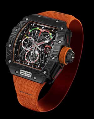
The RM 50-03 watch was made using a unique composite incorporating graphene to manufacture a strong but lightweight new case to house the watch mechanism which weighed just 40 grams in total, including the strap.
The RM 50-03 watch
The RM 50-03 watch.
The collaboration was an exercise in engineering excellence, exploring the methods of correctly aligning graphene within a composite to make the most of the two-dimensional materials superlative properties of mechanical stiffness and strength whilst negating the need for the addition of other, weightier materials.
Now the research behind this unique watch has been published in the journal, Composites Part A: Applied Science and Manufacturing („Realising the Theoretical Stiffness of Graphene in Composites through confinement between Carbon Fibres”). The work was primarily carried out by a group of researchers at The University of Manchester’s National Graphene Institute.
Leading the research Professor Robert Young said: “In this work, through the addition of only a small amount of graphene into the matrix, the mechanical properties of a unidirectionally-reinforced carbon fibre composite have been significantly enhanced.
“This could have future impact on precision-engineering industries where strength, stiffness and product weight are key concerns such in as aerospace and automotive.”
The small amount of graphene used was added to a carbon fibre composite with the goal of improving stiffness and reducing weight by requiring the use of less overall material. Since graphene has high levels of stiffness and strength, its use as a reinforcement in polymer composites shows huge potential of further enhancing the mechanical properties of composites.
The final results were achieved with only a 2% weight fraction of graphene added to the epoxy resin. The resulting composite with graphene and carbon fibre was then analysed by tensile testing and the mechanisms were revealed primarily by using Raman spectroscopy and X-ray CT scans.
The benefits of this research demonstrate a simple method which can be incorporated into existing industrial processes, allowing for engineering industries to benefit from graphene mechanical properties, such as the manufacture of airplane wings or the body work of high-performance cars.
The research group discovered that when comparing with a carbon fibre equivalent specimen, the addition of graphene significantly improved the tensile stiffness and strength. This occurred when the graphene was dispersed through the material and aligned in in the fibre direction.
Dr Zheling Li, a University of Manchester Research Associate said: „This study presents a way of increasing the axial stiffness and strength of composites by simple conventional processing methods, and clarifying the mechanisms that lead to this reinforcement.”
Aurèle Vuilleumier R&D Manager at Richard Mille said: “This project is a perfect example of technology transfer from the university to the product. The partnership with McLaren Applied Technologies allows a broad diffusion of graphene-enhanced composites in the industry. As a tangible result, a world record light and strong watch was available for our customers: the RM 50-03.”
Dr Broderick Coburn, Senior Mechanical Design Engineer at McLaren Applied Technologies said: “The potential of graphene to enhance composites’ structural properties has been known and demonstrated at a lab-scale for some time now. This application, although niche, is a great example of those structural benefits making it through to a prepreg material, and then into an actual product.”
The University of Manchester will soon be celebrating the opening of its second world-class graphene facility, the Graphene Engineering Innovation Centre (GEIC), set-to open later this year. The GEIC will allow industry to work alongside academic expertise to translate research into prototypes and pilot production and accelerate the commercialisation of graphene.
Source: University of Manchester

Cercetatorii dezvolta o metoda pentru mascarea nano-senzori pentru optica si biomedicina(Researchers develop a method for cloaking nano-sensors for optics and biomedicine)

a dezvoltat un model de metamaterial nou, care va îmbunătăți acuratețea nano-senzorilor în optică și biomedicină prin mascarea acestora din exterior radiații.Dezvoltarea unui nou metamaterial de cloaking pentru nano-senzori se realizează în cadrul proiectului italian-rus ANASTASIA (Anatolii invizibile avansate care nu împrăștie radiant și susțin anapoli invizibili).

Posted: Aug 28, 2018

Researchers develop a method for cloaking nano-sensors for optics and biomedicine

(Nanowerk News) An international research group of scientists from Politecnico di Torino (Italy) and NUST MISIS (Russia) has developed a model of a new metamaterial, which will improve the accuracy of nano-sensors in optics and biomedicine by cloaking them from external radiation.

The article reporting the results has been recently published in Scientific Reports („Multipolar passive cloaking by nonradiating anapole excitation”).
The development of a new cloaking metamaterial for nano-sensors is carried out within the framework of the Italian-Russian project ANASTASIA (Advanced Non-radiating Scattering Tenuously Architectures And Sustaining Invisible Anapoles).
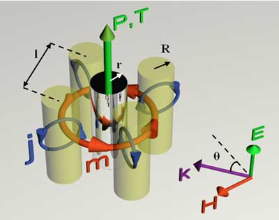
Visualization of a metamolecule, consisting of a PEC cylinder and four dielectric cylinders around
Figure 1: Visualization of a metamolecule, consisting of a PEC cylinder and four dielectric cylinders around. P stands for electric dipole moment of the conductor and T stands for toroidal moment of the dielectric coating
The aim of the project is to model and then prototype a metamaterial, which will make nano-scale objects invisible in the uncovered THz frequency range.
On the part of Politecnico di Torino, Professor Ladislau Matekovits heads the research group, while Professor Alexey Basharin leads the Russian team. In the research, 4 PhD students and other young professionals are also involved.
A cylinder of perfect electric conductor (PEC) with radius r=2.5 µm has been considered in order to imitate a nano-sensor. Being metallic, it possesses very high wave scattering, allowing to carry out calculations for the maximum possible level of re-radiation. The modeling was performed in THz range, which stands between infrared and microwave bands.
The key element of the new metamaterial is a metamolecule (Fig. 1), consisting of four dielectric lithium tantalate (LiTaO3) cylinders, r=5 µm. Serving as a coating for a nano-sensor, dielectrics interact with radiation, exciting non-radiating anapole mode. Separated from each other, all the elements radiate and distort the electric and magnetic fields (Fig. 2 a, b), but when considered all together the object becomes invisible for an external observer (Fig. 2 c).
Visible radiation of elements
Figure 2: Visible radiation of elements, where (a) is the central element without coating; (b) is coating elements without a central element; © is metamolecule: central element in the coating.
Apart from the used LiTaO3, depending on the field of application, other materials can be considered. For example, in nano-optics it would be possible to work with silicon and germanium, while in biomedical sensoring biocompatible sodium chloride would be a possible alternative.
The next research stage, which is the experimental characterization of a prototype of the proposed structure in vitro, is scheduled for this autumn.
Concurrently, interests in creating configurations by using proper materials, e.g., graphene, and geometrical arrangements that are only transparent at certain wavelengths and/or angles of incidence are targeted. The challenge set by scientists from Politecnico di Torino and NUST MISIS is to generalize the experience to develop a theory which can be used to model and then assemble metamaterials that will cloak nano-scaled objects at all the wavelengths and at any angles.
Source: National University of Science and Technology MISIS

Rusia testează armura de putere a robocopului care îi permite soldaților să tragă mitralierele cu o singură mână(Russia tests’robocop’ power armor enabling soldiers to fire machine-guns with one hand)

Un exoskeleton acționat cu motoare electrice integrate și o baterie de stocare testată în Rusia va permite militarilor să lovească cu precizie țintele cu o mitralieră ținută cu o singură mână

Russia tests

Reducerea fricțiunii cu un material de carbon de tip ceapă(Reducing friction with an onion-like carbon material)

În 2015, o echipă de la Argonne National Laboratory a creat un material cu super-lubricitate (aproape zero la frecare) la scară inginerească. Materialul conține grafen și diamante extrem de mici. Echipa a înlocuit grafenul cu disulfură de molibden. Disulfura de molibden provoacă o reacție care transformă diamantele în carbon de tip ceapă.Materialul este un lubrifiant auto-generat, care se reglează continuu, determinându-l să dureze mai mult decât lubrifianții tradiționali uscați

Posted: Aug 27, 2018

Reducing friction with an onion-like carbon material

(Nanowerk News) In 2015, a team from Argonne National Laboratory created a material with superlubricity (near-zero friction) at engineering scale. The material contained graphene and extremely small diamonds. The team replaced the graphene with molybdenum disulfide. The molybdenum disulfide causes a reaction that turns the diamonds into onion-like carbon.

The result? A self-generating, very low friction dry lubricant. As an added bonus, the material lasts much longer than other solid lubricants.
Atomistic simulations of the chemical mechanism leading to reduced friction
Atomistic simulations of the chemical mechanism leading to reduced friction. a–d: Atomic snapshots from simulations at selected times during the sulfur- (S-) induced amorphization of diamond nanoparticles. e–h: Atomic snapshots from simulations at selected times during the formation of onion-like carbon structures. (Image: Badri Narayanan and Subramanian Sankaranarayanan, Argonne National Laboratory)
Superlubricity—a state in which friction essentially disappears—is a highly desirable property. Automobiles and other mechanical assemblies lose efficiency and wear down due to friction. Scientists developed a new material that achieves superlubricity in dry environments. Potential uses include wind turbine gears, magnetic disc drives in computers, and rotating seals. Argonne National Laboratory has three patents on the superlubricity technology. They have a patent pending on the latest breakthrough. It will soon be available for licensing.
In 2015, a multidisciplinary team from Argonne National Laboratory created a material consisting of graphene, nanodiamond particles, and diamond-like carbon that demonstrated superlubricity at the macroscale for the first time. To inform the design of the material, the researchers coupled laboratory experiments at Argonne’s Tribology Laboratory and Center for Nanoscale Materials (CNM) with large-scale molecular dynamics simulations performed at the Argonne Leadership Computing Facility (ALCF) and the National Energy Research Scientific Computing Center (NERSC).
The team has continued to further develop this lubricant technology. Most recently, they replaced the graphene with molybdenum disulfide to explore the impact of using other two-dimensional materials.
In addition to performing detailed experimental investigations of the new material, the researchers carried out simulations on the ALCF’s Mira supercomputer to elucidate its behavior at the nanoscale. Using the LAMMPS (Large-scale Atomic/Molecular Massively Parallel Simulator) code, the team’s large-scale atomistic simulations revealed molecular insights into a mechanical stress-induced tribochemical reaction that led to superlubricity.
They found that the molybdenum disulfide was breaking up into molybdenum and sulfur and reacting with the nanodiamonds to convert them into onion-like carbon structures, which consist of several layers of spherical graphitic shells that can be used as a dry lubricant.
The material is a self-generating lubricant that re-adjusts itself continuously, causing it to last longer than traditional dry lubricants. The team published their findings in Nature Communications.
To enable the computationally demanding molecular dynamics simulations, ALCF staff collaborated with IBM, Lawrence Berkeley National Laboratory, and Sandia National Laboratories to optimize the performance of LAMMPS for Mira and other many-core architectures.

References

D. Berman, B. Narayanan, M.J. Cherukara, S.K.R.S. Sankaranarayanan, A. Erdemir, A. Zinovev, and A.V. Sumant, “Operando tribochemical formation of onion-like-carbon leads to macroscale superlubricity.” Nature Communications 9, 1164 (2018). [DOI: 10.1038/s41467-018-03549-6]
H.M. Aktulga, C. Knight, P. Coffman, K.A. O’Hearn, T.R. Shan, and W. Jiang, “Optimizing the performance of reactive molecular dynamics simulations for many-core architectures.” The International Journal of High Performance Computing Applications (2018). [DOI: 10.1177/1094342017746221]
Source: U.S. Department of Energy, Office of Science

Tehnologia Rostec Active și Passive Exoskeleton în cadrul lucrărilor pentru programul militar rus Ratnik-3 Future Soldier(Rostec Active and Passive Exoskeleton Technology in the Works for Russian Military Ratnik-3 Future Soldier Program)

Ca și cum camuflaj stealth / camuflajul de înclinare vizuală nu este suficient, contractorul rus militar de apărare, Rostec, tocmai a demonstrat „exoschemele pasive operative”

Rostec Active

Tehnologia Rostec Active și Passive Exoskeleton în cadrul lucrărilor pentru programul militar rus Ratnik-3 Future Soldier(Rostec Active and Passive Exoskeleton Technology in the Works for Russian Military Ratnik-3 Future Soldier Program)

Fabricat din fibră de carbon ușoară, materialul pasiv al exoscheletului îmbunătățește capacitățile fizice ale soldatului (forță, viteză etc.), protejând în același timp coloanei vertebrale și articulațiilor – și este reglabil în înălțime. Aceasta permite soldatului să transporte o greutate suplimentară de până la 50 kg (110,231 lbs) în timpul „marșurilor și atacurilor lungi”.Exoskeletonele pasive sunt complet autonome și nu necesită surse de alimentare, servomotoare, electronice și senzori”.

Rostec Active and Passive Exoskeleton Technology in the Works for Russian Military Ratnik-3 Future Soldier Program

As if “stealth camouflage” adaptive camouflage/visual cloaking tech isn’t enough, Russian military defense contractor Rostec just demonstrated “operative passive exoskeletons” for Russian Ratnik-3-type future soldiers/warfighters. Oh, and they’re not done. Rostec is also reportedly developing an active exoskeleton, and they’ve already designed a prototype that’ll be shown at an exhibition, soon. So, it would appear that US military infantry warfighters are going to have their hands full, if World War III (WWIII) ever breaks out, and the Russians are on the opposition.

According to Army Technology, the Rostec passive exoskeleton tech was co-developed by the Central Research Institute for Precision Machine Building (TSNIITOCHMASH), which is part of Russia’s Rostec State, and GB Engineering. Made from lightweight carbon fiber, the passive exoskeleton hardware enhances the soldier’s physical capabilities (strength, speed, etc.), while also protecting his/her spine and joints–and it’s height-adjustable. It enables the soldier to carry up to 50kg (110.231 lbs) extra weight during “long marches and assaults”.

This is the part that intrigues DefenseReview (DR), though:

“The passive exoskeletons are completely autonomous and require no power sources, servomotors, electronics and sensors.”

We’re interested to see how that actually works, and how its capabilities differ from the active exoskeleton tech, which we assume is even more capable in terms of strengh, speed and load-bearing enhancement.

Defense Review will try to glean as much information as possible on Rostec’s active exoskeleton technology, and do a follow-up piece on it. If it weren’t already being used for yogurt, a good name for the technology would be “Activia”–has a nice Russian ring to it.


Company Contact Info:

Rostec
24, Usacheva str.
Moscow, 119048
Russian Federation
Phone: +7 (495) 287-25-25
Email: [email protected]
Website: https://rostec.ru

Cercetătorii dezvoltă un proces nou pentru grafenul 3D(Researchers develop novel process to 3D-print graphene)

Anterior, cercetătorii ar fi putut tipări acest material, cunoscut sub numele de grafen, în foi 2D sau structuri de bază. Însă inginerii Virginia Tech au colaborat acum la un proiect care le permite să tipărească 3D obiecte grafene la o rezoluție cu un ordin de mărime mai mare decât oricând, imprimând astfel posibilitatea de a crea teoretic orice dimensiune sau formă de grafen.Grafenul este un singur strat de atomi de carbon, organizat într-o rețea hexagonală. Atunci când foile de grafen sunt stivuite cu precizie unul peste celălalt și formate într-o formă tridimensională, devine grafit, cunoscut sub numele de „plumb” în creioane.

Posted: Aug 23, 2018

Researchers develop novel process to 3D-print graphene

(Nanowerk News) Researchers from Virginia Tech and Lawrence Livermore National Laboratory have developed a novel way to 3D print complex objects of one of the highest-performing materials used in the battery and aerospace industries.

Previously, researchers could only print this material, known as graphene, in 2D sheets or basic structures. But Virginia Tech engineers have now collaborated on a project that allows them to 3D print graphene objects at a resolution an order of magnitude greater than ever before printed, which unlocks the ability to theoretically create any size or shape of graphene.
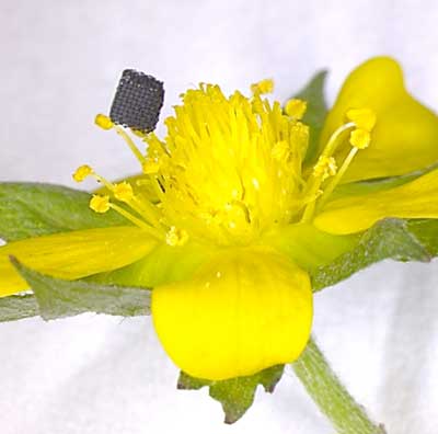
3D-printed graphene octet truss aerogel on strawberry blossom
3D-printed graphene octet truss aerogel on strawberry blossom. (Image: Virginia Tech)
Because of its strength – graphene is one of the strongest materials ever tested on Earth – and its high thermal and electricity conductivity, 3D printed graphene objects would be highly coveted in certain industries, including batteries, aerospace, separation, heat management, sensors, and catalysis.
Graphene is a single layer of carbon atoms organized in a hexagonal lattice. When graphene sheets are neatly stacked on top of each other and formed into a three-dimensional shape, it becomes graphite, commonly known as the “lead” in pencils.
Because graphite is simply packed-together graphene, it has fairly poor mechanical properties. But if the graphene sheets are separated with air-filled pores, the three-dimensional structure can maintain its properties. This porous graphene structure is called a graphene aerogel.
“Now a designer can design three-dimensional topology comprised of interconnected graphene sheets,” said Xiaoyu “Rayne” Zheng, assistant professor with the Department of Mechanical Engineering in the College of Engineering and director of the Advanced Manufacturing and Metamaterials Lab. “This new design and manufacturing freedom will lead to optimization of strength, conductivity, mass transport, strength, and weight density that are not achievable in graphene aerogels.”
Zheng, also an affiliated faculty member of the Macromolecules Innovation Institute, has received grants to study nanoscale materials and scale them up to lightweight and functional materials for applications in aerospace, automobiles, and batteries.
Previously, researchers could print graphene using an extrusion process, sort of like squeezing toothpaste, but that technique could only create simple objects that stacked on top of itself.
“With that technique, there’s very limited structures you can create because there’s no support and the resolution is quite limited, so you can’t get freeform factors,” Zheng said. “What we did was to get these graphene layers to be architected into any shape that you want with high resolution.”
This project began three years ago when Ryan Hensleigh, lead author of the article and now a third-year Macromolecular Science and Engineering Ph.D. student, began an internship at the Lawrence Livermore National Laboratory in Livermore, California. Hensleigh started working with Zheng, who was then a member of the technical staff at Lawrence Livermore National Laboratory. When Zheng joined the faculty at Virginia Tech in 2016, Hensleigh followed as a student and continued working on this project.
scanning electron microscope picture of a graphene octet-truss
Left: Zoomed-in scanning electron microscope picture of a graphene octet-truss at a resolution of 1 micrometer. Right: Zoomed-in scanning electron microscope picture of a graphene octet-truss at a resolution of 10 micrometers. (Image: Virginia Tech)
To create these complex structures, Hensleigh started with graphene oxide, a precursor to graphene, crosslinking the sheets to form a porous hydrogel. Breaking the graphene oxide hydrogel with ultrasound and adding light-sensitive acrylate polymers, Hensleigh could use projection micro-stereolithography to create the desired solid 3D structure with the graphene oxide trapped in the long, rigid chains of acrylate polymer. Finally, Hensleigh would place the 3D structure in a furnace to burn off the polymers and fuse the object together, leaving behind a pure and lightweight graphene aerogel.
“It’s a significant breakthrough compared to what’s been done,” Hensleigh said. “We can access pretty much any desired structure you want.”
The key finding of this work, which was recently published with collaborators at Lawrence Livermore National Laboratory in the journal Materials Horizons („Additive manufacturing of complex micro-architected graphene aerogels”), is that the researchers created graphene structures with a resolution an order of magnitude finer than ever printed. Hensleigh said other processes could print down to 100 microns, but the new technique allows him to print down to 10 microns in resolution, which approaches the size of actual graphene sheets.
“We’ve been able to show you can make a complex, three-dimensional architecture of graphene while still preserving some of its intrinsic prime properties,” Zheng said. “Usually when you try to 3D print graphene or scale up, you lose most of their lucrative mechanical properties found in its single sheet form.”
Source: Virginia Tech
Subscribe to a free copy of one of our daily
Nanowerk Newsletter Email Digests
with a compilation of all of the day’s news.
These articles might interest you as well:

Tranziția de transmisie a tulburărilor aduse se transformă în izolator fotonic topologic(Added disorder drives transition to photonic topological insulator)

Folosind valuri de lumină, cercetătorii au arătat că un sistem non-topologic devine topologic atunci când se adaugă o tulburare aleatorie: nici o lumină nu este transmisă prin interiorul structurii, dar lumina curge peste suprafață într-o manieră unidirecțională.
Sistemul topologic fotonic a fost fabricat prin utilizarea impulsurilor laser concentrate cu densități enorme de energie în gama gigawatt, gravarea ghidurilor de undă într-un mediu de sticlă cu silice de înaltă puritate. Ghidurile de undă au fost aranjate într-o structură de tip grafenie în fagure de miere.
Aceste ghiduri de undă paralele, care ghidează lumina ca fibrele de sticlă, sunt în acest caz proiectate nu ca niște linii drepte ci ca linii elicoidale, astfel încât propagarea luminii în direcția înainte corespunde cu un șurub în sensul acelor de ceasornic și în direcția inversă un șurub invers acelor de ceasornic

Posted: Aug 23, 2018

Added disorder drives transition to photonic topological insulator

(Nanowerk News) Research on insulators with topologically protected surface conductivity – in short: topological insulators – is currently in vogue. Topological materials may be able to replace semiconductor technology in the future.

Topological insulators are characterized by remarkable electrical properties. While these structures have insulating properties in their interior, their conductivity on the surface is extremely robust – to such a degree that in principle an electron current, once introduced, would never cease to flow: one speaks of a „topologically” protected current. Analogous to a stream of electrons, which are half- integer spin particles, so-called fermions, the principle of the topological insulator also works with light particles, so-called bosons, having integer spin.
The properties of a topological insulator are generally stable and persist even when disorder is added. Only a very large disorder in the regular structure can cause the conductive properties on the surface to vanish, resulting in a normal insulator. For photonic topological insulators, this regime of very large disorder means that no light at all can pass through the interior of such a structure, nor can it be transmitted on the surface.
In 2009, Chu, Jain, and Shen theoretically investigated electronic topological insulators with quite extraordinary properties. The starting point of their considerations was a normal insulator, which does not conduct electricity. In their numerical simulation, they showed that the characteristic properties of topological insulators – interior insulation and perfect conductance along the surface (edge) – can be generated by introducing random disorder of the structure. This hypothesis has thus far never been proven in an experiment.
A honeycomb waveguide structure with helical waveguides acts as a photonic topological insulator so that light is guided along the surface
Fig. 1: A honeycomb waveguide structure with helical waveguides acts as a photonic topological insulator so that light is guided along the surface.
In a paper in Nature („Photonic Topological Anderson Insulators”), this hypothesis for electrons in solids was experimentally demonstrated for light waves by an international team of scientists based at the University of Rostock (Germany), the Technion (Israel), as well as Penn State University and the University of Maryland (U.S.). After extensive theoretical considerations and numerically complex simulations, an experimental design was implemented.
Using light waves, the researchers showed that a non-topological system becomes topological when random disorder is added: no light is transmitted through the interior of the structure, but light flows over the surface in a unidirectional fashion.
The photonic topological system was fabricated by using focused laser pulses with enormous energy densities in the gigawatt range, engraving waveguides into a high-purity fused-silica glass medium. The waveguides were arranged in a honeycomb graphene structure.
These parallel waveguides, which guide the light like glass fibers, are in this case designed not as straight lines but as helical lines, so that the propagation of the light in the forward direction corresponds to a clockwise screw and in the reverse direction a counterclockwise screw. This creates the diffraction properties of a topological insulator, where light circulates around the circumference of the helical array of waveguides in a single direction, and in a way that is immune to disorder such as a missing waveguide (Fig. 1).
However, when the helical honeycomb lattice is systematically modified so that the refractive index of adjacent waveguides is slightly different, the topological properties are destroyed: the light no longer flows on the surface in a unidirectional manner (Fig. 2). When a random disorder is added on top of this modified structure, the topological properties are fully recovered.
Adding further disorders to the refractive indices of the waveguides restores the topological properties so that light flows again along the surface of the structure
Fig. 2: Adding further disorders to the refractive indices of the waveguides restores the topological properties so that light flows again along the surface of the structure.
In the experimental setup, light from a red Helium Neon laser is coupled into the waveguide structure. At the other end of the waveguide structure, a camera detects whether light is transmitted through the structure or is transmitted on the surface. In a first experiment, the refractive indices of every adjacent waveguides were made to differ by two ten thousandths. Thus the conductive properties of the topological structure were completely destroyed: no light could be detected behind the structure. But what happens if further disorders are added to the existing disorder?
In a second experiment, the waveguides were prepared in such a way that irregularly distributed differences in the refractive indices of all waveguides were added to the existing regular disorder of adjacent waveguides. Contrary to the expectation that in the event of further disorder in the topological structure the purely insulating properties would be retained and it would remain dark in the sample, the second experiment showed light conduction across the surface. Light could indeed be detected at the edge.
Thus, in the case of light, the experimental proof of the hypothesis of Chu et al., which had originally been expressed only for electrons, has succeeded: by adding disorder, topological insulators can be generated from normal insulators, a highly counterintuitive result. The properties of topological materials as such are quite remarkable; however the dependence of their properties on disorder in the structure is even more extraordinary.
The novel findings of the international research group may contribute to further elucidating the bizarre properties of topological insulators.
“These findings shed new light onto the peculiar properties of topological insulators,” said Professor Alexander Szameit, principal investigator of the Rostock group and lead author of the publication. “This shows that using photonics, we have opened the door to understanding disordered topological insulators in a completely new way. Photonic topological systems could potentially be a route to overcoming parasitic disorder in both fundamental science and real-world applications.”
Professor Mordechai Segev of the Technion added: “The first photonic topological insulator for light was realized in 2013 through collaboration between my group, where the research was led by Mikael Rechtsman and Yonatan Plotnik, and the group of Alex Szameit (at that time in Jena, Germany). Two years later, Mikael Rechtsman and my young colleague Netanel Lindner wrote a theory paper that envisioned the current experiment. And now the experiment has become a reality through the efforts of Alex’s students in a beautiful paper which we all collaborated on. It is fascinating to see how this new field is being led by a group of young, very talented people like Mik, Netanel, Alex and their students, in three different countries.”
Source: Universität Rostock

Conductele laminate de la Graphene ar putea reduce coroziunea în industria de petrol și gaze(Graphene laminated pipes could reduce corrosion in the oil and gas industry)

Grafenul este primul material bidimensional din lume, flexibil, transparent, mai conductiv decât cuprul și este cunoscut că blochează trecerea heliului, cel mai greu gaz de blocat.Cercetătorii au descoperit că dacă grafenul a fost amestecat mecanic cu materialul plastic sau dacă s-a aplicat un singur strat de grafen, gazele ar fi putut să treacă.
Cu toate acestea, prin laminarea unui strat subțire de nanoplateste de grafen la poliamida 11 (PA11) – un material plastic folosit adesea în aceste căptușeli – echipa a reușit să producă structuri care se comportă ca niște bariere excepțional de bune.

Posted: Aug 22, 2018

Graphene laminated pipes could reduce corrosion in the oil and gas industry

(Nanowerk News) Researchers at The University of Manchester and TWI have discovered ways of using graphene to prolong the lifetime of pipes used in the oil and gas industry.

Published in Advanced Materials Interfaces („Graphene/Polyamide Laminates for Supercritical CO2 and H2S Barrier Applications: An Approach toward Permeation Shutdown „), the team have found a way of incorporating graphene into a polymer liner used in pipes that transport crude oil and gas from the sea floor.
The pipes are generally made of internal layers of polymer or composite and external strengthening steel. Within these pipes, fluids may be at very high pressure and elevated temperature.
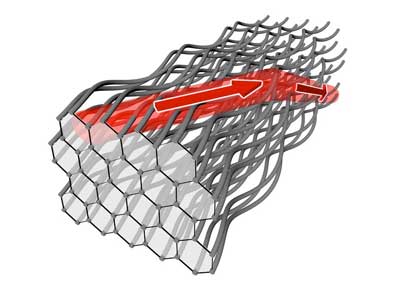
using graphene to prolong the lifetime of pipes used in the oil and gas industry
Using graphene to prolong the lifetime of pipes used in the oil and gas industry. (Image: University of Manchester)
In situations where carbon dioxide (CO2), hydrogen sulfide (H2S) and water permeate through the protective barrier layer of the pipe, the steel may corrode causing the pipe to lose strength over time, leading to a risk of catastrophic failure.
The researchers found that if the graphene was mechanically mixed with the plastic, or if a single layer of graphene were applied, gases were still able to pass through.
However, by laminating a thin layer of graphene nanoplatelets to polyamide 11 (PA11) – a plastic often used in these liners – the team were able to produce structures that behave as exceptionally good barriers.
The multi-layered laminate structures were tested at 60°C and at pressures up to 400 times atmospheric pressure, and were shown to reduce CO2 permeation by over 90% compared to PA11 alone, while permeation of H2S can be reduced to undetectable levels.
Graphene is the world’s first two-dimensional material, flexible, transparent, more conductive than copper, and is known to block the passage of helium, the hardest gas to block.
Corrosion costs the oil and gas industry in the US alone $1.4 billion. This technology has the potential to extend the life of the underwater pipework and therefore reduce the time between repairs.
Professor Peter Budd, who led the Manchester team, said: “Graphene has many amazing properties, but it is not always easy to realise them on a large scale. Our work represents an important step in taking graphene out of the laboratory and into the real world.”
Dr Paul Woollin, Director of Research, TWI, said: “This research is an example of how TWI can work effectively with world leading universities through its Innovation Network, and draw on our cutting edge testing capability and in house experts, to identify unique and novel solutions to industry’s most challenging problems.
Graphene membranes such as these have the potential to open up vast new markets and revolutionise countless industrial processes, such as food packaging, water filtration and gas separation.
Source: University of Manchester

Insulatorul topologic nou ar putea îmbunătăți eficiența procesării și memoriei computerului(New topological insulator could improve efficiency of computer processing and memory)

O echipă de cercetători condusă de Universitatea din Minnesota a dezvoltat un nou material care ar putea îmbunătăți eficiența procesării și memoriei computerului. Cercetatorii au depus un brevet asupra materialului cu sprijinul companiei de cercetare Semiconductor Corporation, iar oamenii din industria semiconductorilor au cerut deja mostre din material.Noul material se află într-o clasă de materiale numite „izolatoare topologice”, care au fost studiate recent de comunitățile de cercetare fizică și materiale și de industria semiconductorilor datorită transportului unic spin-electronic și proprietăților magnetice.

Posted: Aug 22, 2018

New topological insulator could improve efficiency of computer processing and memory

(Nanowerk News) A team of researchers led by the University of Minnesota has developed a new material that could potentially improve the efficiency of computer processing and memory. The researchers have filed a patent on the material with support from the Semiconductor Research Corporation, and people in the semiconductor industry have already requested samples of the material.

The findings are published in Nature Materials („Room-temperature high spin–orbit torque due to quantum confinement in sputtered BixSe(1–x) films”), a peer-reviewed scientific journal published by Nature Publishing Group.
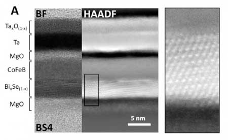
cross-sectional transmission electron microscope image shows a sample used for the charge-to-spin conversion experiment
This cross-sectional transmission electron microscope image shows a sample used for the charge-to-spin conversion experiment. The nano-sized grains of less than 6 nanometers in the sputtered topological insulator layer created new physical properties for the material that changed the behavior of the electrons in the material. (Image: Wang Group, University of Minnesota)
“We used a quantum material that has attracted a lot of attention by the semiconductor industry in the past few years, but created it in unique way that resulted in a material with new physical and spin-electronic properties that could greatly improve computing and memory efficiency,” said lead researcher Jian-Ping Wang, a University of Minnesota Distinguished McKnight Professor and Robert F. Hartmann Chair in electrical engineering.
The new material is in a class of materials called “topological insulators,” which have been studied recently by physics and materials research communities and the semiconductor industry because of their unique spin-electronic transport and magnetic properties. Topological insulators are usually created using a single crystal growth process. Another common fabrication technique uses a process called Molecular Beam Epitaxy in which crystals are grown in a thin film. Both of these techniques cannot be easily scaled up for use in the semiconductor industry.
In this study, researchers started with bismuth selenide (Bi2Se3), a compound of bismuth and selenium. They then used a thin film deposition technique called “sputtering,” which is driven by the momentum exchange between the ions and atoms in the target materials due to collisions. While the sputtering technique is common in the semiconductor industry, this is the first time it has been used to create a topological insulator material that could be scaled up for semiconductor and magnetic industry applications.
However, the fact that the sputtering technique worked was not the most surprising part of the experiment. The nano-sized grains of less than 6 nanometers in the sputtered topological insulator layer created new physical properties for the material that changed the behavior of the electrons in the material. After testing the new material, the researchers found it to be 18 times more efficient in computing processing and memory compared to current materials.
“As the size of the grains decreased, we experienced what we call ‘quantum confinement’ in which the electrons in the material act differently giving us more control over the electron behavior,” said study co-author Tony Low, a University of Minnesota assistant professor of electrical and computer engineering.
Researchers studied the material using the University of Minnesota’s unique high-resolution transmission electron microscopy (TEM), a microscopy technique in which a beam of electrons is transmitted through a specimen to form an image.
“Using our advanced aberration-corrected scanning TEM we managed to identify those nano-sized grains and their interfaces in the film,” said Andre Mkhoyan, a University of Minnesota associate professor of chemical engineering and materials science and electron microscopy expert.
Researchers say this is only the beginning and that this discovery could open the door to more advances in the semiconductor industry as well as related industries, such as magnetic random access memory (MRAM) technology.
“With the new physics of these materials could come many new applications,” said Mahendra DC (Dangi Chhetri), first author of the paper and a physics Ph.D. student in Professor Wang’s lab.
Wang agrees that this cutting-edge research could make a big impact.
“Using the sputtering process to fabricate a quantum material like a bismuth-selenide-based topological insulator is against the intuitive instincts of all researchers in the field and actually is not supported by any existing theory,” Wang said. “Four years ago, with a strong support from Semiconductor Research Corporation and the Defense Advanced Research Projects Agency, we started with a big idea to search for a practical pathway to grow and apply the topological insulator material for future computing and memory devices. Our surprising experimental discovery led to a new theory for topological insulator materials.
“Research is all about being patient and collaborating with team members. This time there was a big pay off,” Wang said.
Source: University of Minnesota College of Science and Engineering