Procedura de nanosculptare pentru îmbinarea metalelor fără sudură(Nanosculpturing process to join metals without welding)

În schimb, procesul dezvoltat de grupul de cercetare al Universității din Kiel, condus de profesorul Rainer Adelung, nu numai că economisește materialele care urmează să fie alăturate, dar este și mai ușor și mai flexibil de utilizat, chiar și în locuri greu accesibile, cum ar fi colțurile sau partea superioară în jos pe tavan. În doar câteva minute, metalele pot fi conectate permanent între ele, dar și cu polimeri.

Posted: Apr 24, 2018

Nanosculpturing process to join metals without welding

(Nanowerk News) Welding is still the standard technique for joining metals. However, this laborious process carried out at high temperatures is not suitable for all applications. Now, a research team from the „Functional Nanomaterials” working group at Kiel University, together with the company Phi-Stone AG from Kiel, has developed a versatile alternative to conventional welding and gluing processes. Based on a special etching process, it enables aluminium and aluminium alloys to be joined with each other as well as with polymers, forming a durable and strong joint (Nanoscale Horizons, „Making metal surfaces strong, resistant, and multifunctional by nanoscale-sculpturing”).

They will present the prototype of a mobile joining unit at the Hannover Messe (23 – 27 April). They plan to commence mass production in future, after feedback from customers.
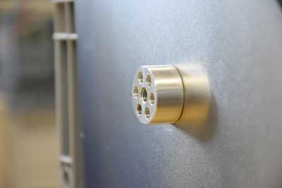
aluminium flange attached to an aluminium wall
The aluminium flange is firmly attached to the aluminium wall. (Image: Siekmann, CAU)
When welding, components are joined by locally melting them at the connection point. However, the high temperatures required for this influence the material in the so-called heat-affected zone, causing structural as well as optical changes. It also requires special safety precautions and appropriately qualified staff.
In contrast, the process developed by the Kiel University research group led by Professor Rainer Adelung not only spares the materials to be joined, but it is also easier and more flexible to use, even in hard-to-reach places such as corners or upside down on the ceiling. In just a few minutes, metals can be permanently connected with each other, but also with polymers.
The team envisages areas of application such as ship, aircraft or vehicle production. The process is particularly well-suited for subsequently attaching components in existing constructions, for example, in the interiors of ships or cars, explained Adelung regarding possible applications.
„The high temperatures of welding will destroy surfaces that have already been treated and painted, for example. Our process, on the other hand, works at room temperature without special protective measures,” said Adelung.
To be able to connect metals, the Kiel research team uses its „nanoscale sculpturing” process to roughen the surface with a precise electro-chemical etching procedure, so that a fine, rectangular hook structure is created on the micrometre level. When two of these treated surfaces are inter-locked using an adhesive, a strong joint is created which is very difficult to break.
„If something breaks at all, then perhaps the actual adhesive or the material itself, but not the connection point”, said Ingo Paulowicz, board member of Phi-Stone AG. „The nanoscale sculpturing process thus opens up completely new possibilities in the field of joining technology, but also entirely new combinations of materials, such as aluminium with copper or with silicone. This could be interesting for medical technology, for example,” added Adelung.
In order to use this joining process in industry, the Kiel University team and Phi-Stone AG have now developed a mobile and easy-to-use prototype called „Metalangelo”. Using customised etching cells produced via 3D printing, metal surfaces can be precisely processed at room temperature. Together with their first customers, they want to include customer requirements and develop the prototype to market-readiness. Two patents have already been registered in this regard.
The name of the prototype references to the renaissance sculptor Michelangelo, and emphasises the basic principle of the new process: the directed modification of surfaces – in the case of the Kiel research team, however, metal instead of marble.
From 23 – 27 April 2018, the research team will present its prototype at the Kiel University booth at the Hannover Messe, and demonstrate the process daily, live at 1:30pm (Hall 2, Research & Technology, Booth C07). Professor Rainer Adelung will also present the new connection process in a lecture on Tuesday 24 April 2005 at 2pm and 4pm.
Source: Christian-Albrechts-Universität zu Kiel

Hexapod rapid, de înaltă încărcare pentru simulare de mișcare, stabilizare și anulare

Noul HEXAPODAL compact este de călătorie liniară variază de până la 200mm și rotația la 66 de grade. Acesta este condus de brushless servomotoare și combină o capacitate de încărcare mare (130 lbs), cu răspuns rapid și viteze liniare mari de până la 80mm / sec și viteza unghiulară de 30 ° / sec. Paralel Designul cinematicii elimina necesitatea cablurilor și a rezultatelor se deplasează într-o soluție de poziționare foarte rigid și compact, în comparație cu convenționale modele multi-axe.

Posted: Apr 29, 2016

Fast, High-Load Hexapod for Motion Simulation, Stabilization, and Cancellation

(Nanowerk News) PI (Physik Instrumente) LP, a leading manufacturer of precision positioning, motion control and nanopositioning equipment, introduces the H-900KSCO hexapod, designed dynamic motion in XYZ, pitch roll, and yaw. 6-axis parallel kinematics motion is perfected by PI hexapods delivering nanopositioning precision, high speed, and stability necessary to meet today’s demanding motion control applications.
H-900KSCO hexapod
H-900KSCO hexapod
Applications of H-900KSCO Hexapod
Hexapod applications include motion simulation (profiles compatible to ISO 20672, ISO 8728, and ISO 16328), industrial production, precision machining, automotive industry, stabilization of motion on moving vehicles and vessels.
Compact & Stiff, No Moving Cables
The new compact hexapod provides linear travel ranges up to 200mm and rotation to 66 degrees. It is driven by brushless servo-motors and combines high load capacity (130 lbs) with fast response and high linear speeds up to 80mm/sec and angular speed of 30°/sec. The parallel kinematics design eliminates the need for moving cables and results in a very stiff and compact positioning solution, compared to conventional multi-axis designs.
Watch video on versatility of PI Hexapods
Specifications, Datasheet, More Information
Standard and Custom
PI has in-house engineered solutions with over 4 decades of experience working with customers to provide products that meet application demands, and can quickly modify existing product designs or provide a fully customized OEM part to fit the exact requirements of the application.
Features & Advantages
  • Low-Wear, Brushless DC Motor
  • Load Up to 60kg
  • Travel Ranges to 200mm (linear), 66° (rotation)
  • Speed: 80mm/sec (linear), 30°/sec (angular)
About PI
PI is a leading manufacturer of precision motion control equipment, piezo motors, air bearing stages and hexapod parallel-kinematics for semiconductor applications, photonics, bio-nano-technology and medical engineering. PI has been developing and manufacturing standard & custom precision products with piezoceramic and electromagnetic drives for 4 decades. The company has been ISO 9001 certified since 1994 and provides innovative, high-quality solutions for OEM and research. PI is present worldwide with eleven subsidiaries, R&D / engineering on 3 continents and total staff of 850.
Source: PI (press release)

Read more: Fast, High-Load Hexapod for Motion Simulation, Stabilization, and Cancellation

Îmbunătățirea măsurătorilor CD-AFM de la vârf în jos

Probele finale au fost distribuite companiilor membre SEMATECH. Produsul final a fost o bucată de 1 cm2 de siliciu cu ținte multiple de măsurare cufundate în centrul unei plachete de 200 mm. Inainte de acest efort NIST, cercetatorii au folosit o varietate de produse comerciale pentru a încerca să calibreze sfaturi lor AFM. Unele dintre soluțiile au avut tendința de a deteriora vârfurile instrumentului. În cazul în care vârful a supraviețuit procesului, produsele au fost doar in masura sa ofere incertitudinea de aproximativ 5 nm. Alți oameni de știință din industrie ar folosi mostre de producție cu valori cunoscute pentru a încerca calibrare sfat, obtinandu-se incertitudinea de aproximativ 5 nm. Probele fabricate de NIST echipa umplut o nevoie critică în industrie, în cazul în care standardele acceptabile pentru calibrarea lățimii vârfului AFM nu au fost disponibile.

Posted: Mar 31, 2016

Improving CD-AFM measurements from the tip down

(Nanowerk News) As the sizes of computer chips in electronic devices continue to shrink, traditional measurement tools (e.g., microscopes utilizing visible light) are no longer capable of examining surface features, which can be just tens of nanometers. In order to examine these tiny features, researchers use tools such as the critical dimension atomic force microscope (CD-AFM), which measures features by dragging its ∼10 nm tip across the subject’s surface much like a record player needle pulling across a record’s grooves. With its extremely high accuracy—potential width uncertainty as low as 1 nm—the CD-AFM is the tool of choice for numerous scientists in the semiconductor industry. However, accurate measurements using the CD-AFM are entirely dependent on whether the instrument’s tip is properly calibrated. To address this critical need, PML researchers, led by the Engineering Physics Division’s Ron Dixson, have created reference samples that allow tip calibration with an uncertainty of less than 1 nm.

 Scanning electron microscope image of a SCCDRM sample, displaying the pattern of near-vertical sidewalls with varying linewidths, high uniformity, and known linewidth values
Figure 1. Scanning electron microscope image of the SCCDRM sample, displaying the pattern of near-vertical sidewalls with varying linewidths, high uniformity, and known linewidth values.
“With an AFM, linewidth calibration and tip-width calibration are basically synonymous,” Dixson says. “A linewidth measurement with an AFM depends entirely on the tip calibration.”
When examining the raw data from a CD-AFM, The apparent linewidths actually include the width of the tip. The tip width is then subtracted from the image to provide the final data. If the user believes the tip width is 10 nm but it is actually 15 nm, the uncertainty of the tool’s measurements can rise to an unacceptable level.
So, how do you know the precise measurement of a nanometer-sized tip when the tool in question is one of the only ways of measuring a feature that small?
Dixson and his colleagues have been working periodically over the past 10 to 15 years on a solution to calibrate CD-AFM tips. The first NIST standard for this calibration was created by the team back in 2005 („Traceable calibration of critical-dimension atomic force microscope linewidth measurements with nanometer uncertainty”), and it provided a tip width uncertainty of approximately 1 nm. This was the result of a fruitful collaboration between NIST and SEMATECH that sent Dixson on assignment at SEMATECH for three years starting in late 2001.
“We didn’t have a CD-AFM at NIST,” Dixson explains. “We had no real AFM linewidth measurement capability, and we weren’t actually expecting that we would get it. Those instruments cost over a million dollars at the time. SEMATECH had an AFM, and they didn’t actually have anyone there to run it at the time. We had AFM experts at NIST, and they had an AFM.” Thus, the collaboration was born.
During this initial research period, Dixson and his colleagues used the CD-AFM and a transmission electron microscope (TEM) in concert to calibrate the samples. This was done by using CD-AFM as a comparator between the samples sacrificed for TEM and those distributed to end users. Although the TEM is a destructive measurement technique, it creates images that allow the researcher to count the atomic planes of the sample.* The NIST researchers were able to measure samples with the non-destructive CD-AFM and anchor the results to the SI meter using measurements with high resolution TEM.
The final samples were distributed to SEMATECH member companies. The end product was a 1 cm2 piece of silicon with multiple measurement targets sunk into the center of a 200 mm wafer. Prior to this NIST effort, researchers used a variety of commercial products to attempt to calibrate their AFM tips. Some of the solutions had a tendency to damage the instrument tips. If the tip survived the process, the products were only able to offer an uncertainty of approximately 5 nm. Other industry scientists would use production samples with known values to attempt tip calibration, again achieving uncertainty of approximately 5 nm. The samples fabricated by the NIST team filled a critical need in the industry, where acceptable standards for calibration of AFM tip width were unavailable.
“The uncertainty was roughly 1 nm,” Dixson says. “The description is approximate because there were only a few chips from that generation that had that precise uncertainty. The majority of the samples had uncertainties closer to 1.5 or 2 nm.”** The difference between samples was due to the variation in linewidth along the features, which were not quite uniform.
Recently, after revisiting the sample fabrication process, the NIST team improved upon the results, creating reference samples that are more consistent from chip to chip and can provide an uncertainty of less than 1 nm („Process optimization for lattice-selective wet etching of crystalline silicon structures”).
 Scanning electron microscope image of a CDR50 type CD-AFM tip
Figure 2. Scanning electron microscope image of a CDR50 type CD-AFM tip. These tips have a nominal geometric width of 50 nm, but the width must be calibrated for each tip.
“The improvement of the new samples is up to a factor of five, taking into account the non-uniformity of earlier ones versus the new ones using the better etching process.”
Like the sample back in 2005, the new reference sample is a single crystal dimension reference material (SCCDRM), which was fabricated using a lattice-plane-selective etch on (110) silicon. Essentially, a pattern of near-vertical sidewalls with varying linewidths, high uniformity, and known values was etched onto a chip (see Figure 1). A user can calibrate a CD-AFM tip by measuring the sample, comparing it to the known value, and making adjustments as necessary.
“In most AFMs, the user has the capability of inputting the known tip width into the tool,” Dixson explains. If the user enters a value and then measures the sample, the results would indicate whether the known tip width is actually accurate.
The improvement of this latest batch of samples can be traced back to the use of potassium hydroxide (KOH) as the etchant instead of the previously used tetramethyl ammonium hydroxide. During the fabrication process, an oxide hard mask is applied to the chip surface. Before the sample can be completed, as much of the hard mask as possible needs to be removed. The KOH etchant was extremely successful at removing the oxide mask without damaging the narrow sidewalls, maintaining the precise features of the structure. On the 2005 samples, the dimensions of the sidewalls were not uniform throughout their lengths, which made user error a possibility if the tip was not placed at a precisely defined spot along the sidewall.
Since this research was completed, Dixson participated in a comparative study with PTB (Physikalisch-Technische Bundesanstalt, the National Metrology Institute of Germany). PTB was also working on a similar calibration solution for CD-AFMs, and it made sense for the two institutes to cross-check their samples. The soon-to-be-published results indicated that the samples from the two institutes had very similar levels of uncertainty.
Samples from the NIST team’s new and improved effort have not been widely distributed at this time. A wider distribution is under consideration. In addition, a future focus on providing additional CD-AFM tip calibrations is being discussed.
“We might explore the possibility of calibrating the vertical edge height,” Dixson says. “That is the distance between the base of the tip and the point that contacts the sample. There is no official standard available for this.”
Notes
*Strictly speaking, the HRTEM image does not allow the researcher to count the atoms. The researcher is actually counting interference fringes. But, there is a one-to-one correspondence with the atomic planes.
**The NIST master sample from the project is known to 0.6 nm (k = 2), but the added uncertainty due to the transfer process meant that the distributed samples all had larger uncertainties.
Source: NIST

Read more: Improving CD-AFM measurements from the tip down

Controlerul piezo-digital de înaltă performanță PI de înaltă performanță este prea eficient din punct de vedere al costurilor

Specificații, foaie de date, mai multe informații
Aplicațiile E-727
Aplicațiile includ nanopoziția, nano-automatizarea, tehnologia semiconductorilor, fotonica, bio-nanotehnologia, metrologia, microscopia, micro-manipularea, inclusiv aplicațiile curate.
Caracteristici și avantaje
– Servo Digital pentru algoritmi avansați de control
– Lățime de bandă de control de 25 kHz
– Pentru senzori de feedback cu capacitate și piezo-rezistență
– Intrări și ieșiri de control analogic de înaltă rezoluție
– Interfețe: Ethernet, USB și RS-232
– Intrări și ieșiri digitale
– DSP 32/64-bit, Floating Point, 375 MHz
– DAC pe 20 biți și rezoluție ADC
– ID Chip compatibil pentru interschimbabilitatea controlerului și a mecanicii
– Linia 4 din ordinul polinomial


Posted: Feb 29, 2016

PI’s New High Performance Multi-Channel Digital Piezo Controller is Cost-Effective Too

(Nanowerk News) PI (Physik Instrumente) L.P., an industry leader in precision motion components, systems, and solutions, has released a new, high-performance 3 and 4-channel digital piezo controller that integrates with a wide range of existing piezo-based nanpositioning systems and piezo actuators.
E-727 controller
Lower Price, Higher Performance
The new E-727 replaces the E-725 controller and combines higher performance with a lower price. Compared to its predecessor, it provides 3 additional high-resolution analog interfaces, a faster servo, as well as a broader choice of traditional, high-speed, and real time digital interfaces, such as SPI, Ethernet, USB and RS-232
Ultra-Low Noise Controller
20-bit DAC & ADC converters keep the closed-loop E-727 controller operating with high resolution and ultra-low noise, along with 4 integrated power amplifiers for multilayer piezo drives with operating voltage of -30 to +130V. Closed-loop nanopositioning systems are supported with capacitive feedback sensors, piezoresistive sensors, and traditional strain gauges. In addition to PID control, 2 additional user programmable notch filters are implemented for suppression of mechanical system resonances. Linearization based on 4th order polynomials provides higher positioning accuracy. The Dynamic Digital Linearization (DDL) feature eliminates non-linearities at high operating frequencies.
Data Recorder, Auto-Calibration ID Chip, Quick Start UP, Comprehensive Software Package The cost-effective E-727 has a data recorder for high speed tracing, ID chip compatibility for quick start-up, and exchange of system components without recalibration, and the additional feature of programmable drift compensation. The controller comes with extensive software support for LabVIEW and shared libraries for Windows and Linux. Multiple digital interfaces for ease of control: Ethernet, USB, RS-232, SPI. Four (4) digital I/O channels as well as four (4) high-resolution analog inputs and outputs each are also available for use with external sensors, target values or external amplifiers.
Specifications, Datasheet, More Information
Applications of the E-727
Applications include nanopositioning, nano-automation, semiconductor technology, photonics, bio-nano-technology, metrology, microscopy, micro-manipulation, including cleanroom applications.
Features & Advantages
  • – Digital Servo for Advanced Control Algorithms
  • – 25 kHz Control Bandwidth
  • – For Capacitive and Piezo-restive Strain Gauge Feedback Sensors
  • – High Resolution Analog Control Inputs and Outputs
  • – Interfaces: Ethernet, USB, and RS-232
  • – Digital Inputs and Outputs
  • – DSP 32/64-bit Floating Point, 375 MHz
  • – 20-bit DAC and ADC Resolution
  • – ID Chip Compatible for Interchangeability of Controller and Mechanics
  • – 4th Order Polynomial Linearization for Mechanics & Electronics
About PI
PI is a leading manufacturer of precision motion control equipment, piezo motors, air bearing stages and hexapod parallel-kinematics for semiconductor applications, photonics, bio-nano-technology and medical engineering. PI has been developing and manufacturing standard & custom precision products with piezoceramic and electromagnetic drives for 4 decades. The company has been ISO 9001 certified since 1994 and provides innovative, high-quality solutions for OEM and research. PI is present worldwide with eleven subsidiaries, R&D / engineering on 3 continents and total staff of 800+.
Source: PI (press release)

Read more: PI’s New High Performance Multi-Channel Digital Piezo Controller is Cost-Effective Too