Bolometrul nou de grafen este mai rapid, mai simplu și acoperă mai multe lungimi de undă(New graphene bolometer is faster, simpler, and covers more wavelengths)

Există o cerere imensă pentru noile tehnologii de detectare în infraroșu cu sensibilitate ridicată. Această lucrare a lui Efetov și co-lucrătorilor care raportează un bolometru inovator de grafen, integrat într-o cavitate de cristal fotonic pentru a obține o absorbție ridicată, este oportună și interesantă.

Posted: Jun 11, 2018

New graphene bolometer is faster, simpler, and covers more wavelengths

(Nanowerk News) Bolometers, devices that monitor electromagnetic radiation through heating of an absorbing material, are used by astronomers and homeowners alike. But most such devices have limited bandwidth and must be operated at ultralow temperatures. Now, researchers say they’ve found a ultrafast yet highly sensitive alternative that can work at room temperature — and may be much less expensive.

The findings, published in the journal Nature Nanotechnology („Fast thermal relaxation in cavity-coupled graphene bolometers with a Johnson noise read-out”), could help pave the way toward new kinds of astronomical observatories for long-wavelength emissions, new heat sensors for buildings, and even new kinds of quantum sensing and information processing devices, the multidisciplinary research team says. The group includes recent MIT postdoc Dmitri Efetov, Professor Dirk Englund of MIT’s Department of Electrical Engineering and Computer Science, Kin Chung Fong of Raytheon BBN Technologies, and colleagues from MIT and Columbia University.
graphene bolometer
Schematic illustration of the experimental setup. (Image: Courtesy of the researchers)
“We believe that our work opens the door to new types of efficient bolometers based on low-dimensional materials,” says Englund, the paper’s senior author. He says the new system, based on the heating of electrons in a small piece of a two-dimensional form of carbon called graphene, for the first time combines both high sensitivity and high bandwidth — orders of magnitude greater than that of conventional bolometers — in a single device.
“The new device is very sensitive, and at the same time ultrafast,” having the potential to take readings in just picoseconds (trillionths of a second), says Efetov, now a professor at ICFO, the Institute of Photonic Sciences in Barcelona, Spain, who is the paper’s lead author. “This combination of properties is unique,” he says.
The new system also can operate at any temperature, he says, unlike current devices that have to be cooled to extremely low temperatures. Although most actual applications of the device would still be done under these ultracold conditions, for some applications, such as thermal sensors for building efficiency, the ability to operate without specialized cooling systems could be a real plus. “This is the first device of this kind that has no limit on temperature,” Efetov says.
The new bolometer they built, and demonstrated under laboratory conditions, can measure the total energy carried by the photons of incoming electromagnetic radiation, whether that radiation is in the form of visible light, radio waves, microwaves, or other parts of the spectrum. That radiation may be coming from distant galaxies, or from the infrared waves of heat escaping from a poorly insulated house.
The device is entirely different from traditional bolometers, which typically use a metal to absorb the radiation and measure the resulting temperature rise. Instead, this team developed a new type of bolometer that relies on heating electrons moving in a small piece of graphene, rather than heating a solid metal. The graphene is coupled to a device called a photonic nanocavity, which serves to amplify the absorption of the radiation, Englund explains.
“Most bolometers rely on the vibrations of atoms in a piece of material, which tends to make their response slow,” he says. In this case, though, “unlike a traditional bolometer, the heated body here is simply the electron gas, which has a very low heat capacity, meaning that even a small energy input due to absorbed photons causes a large temperature swing,” making it easier to make precise measurements of that energy. Although graphene bolometers had previously been demonstrated, this work solves some of the important outstanding challenges, including efficient absorption into the graphene using a nanocavity, and the impedance-matched temperature readout.
The new technology, Englund says, “opens a new window for bolometers with entirely new functionalities that could radically improve thermal imaging, observational astronomy, quantum information, and quantum sensing, among other applications.”
For astronomical observations, the new system could help by filling in some of the remaining wavelength bands that have not yet had practical detectors to make observations, such as the “terahertz gap” of frequencies that are very difficult to pick up with existing systems. “There, our detector could be a state-of-the-art system” for observing these elusive rays, Efetov says. It could be useful for observing the very long-wavelength cosmic background radiation, he says.
Daniel Prober, a professor of applied physics at Yale University who was not involved in this research, says, “This work is a very good project to utilize the many benefits of the ultrathin metal layer, graphene, while cleverly working around the limitations that would otherwise be imposed by its conducting nature.” He adds, “The resulting detector is extremely sensitive for power detection in a challenging region of the spectrum, and is now ready for some exciting applications.”
And Robert Hadfield, a professor of photonics at the University of Glasgow, who also was not involved in this work, says, “There is huge demand for new high-sensitivity infrared detection technologies. This work by Efetov and co-workers reporting an innovative graphene bolometer integrated in a photonic crystal cavity to achieve high absorption is timely and exciting.”
Source: By David Chandler, MIT

Tehnica neașteptată pentru a detecta agenții chimici de război (Unexpexted Technique to Detect Chemical Warfare agents)

Oferind un mijloc inovator, ieftin și rapid de detectare a agenților de amenințare, o nouă tehnologie de detectare poate oferi avantaje semnificative pentru războinicii desfășurați

Unexpected

O fibră elastică umplute cu electrozi care să revoluționeze hainele inteligente(An elastic fiber filled with electrodes set to revolutionize smart clothes)

Este un mod cu totul nou de a gândi despre senzori. Fibrele mici dezvoltate la EPFL sunt fabricate din elastomer și pot încorpora materiale cum ar fi electrozi și polimeri nanocompoziți. Fibrele pot detecta chiar și cea mai mică presiune și tensiune și pot rezista la deformări de aproape 500% înainte de a-și recupera forma inițială. Tot ceea ce le face perfecte pentru aplicații în îmbrăcăminte și proteze inteligente și pentru crearea de nervi artificiali pentru roboți.deformate, dar întotdeauna se întorc la forma lor originală.
Materiale rigide precum polimerii nanocompozite, metalele și termoplastele pot fi introduse în fibre, precum și metalele lichide care pot fi ușor deformate. „De exemplu, putem adăuga trei șiruri de electrozi în partea superioară a fibrelor și una în partea inferioară.Electrodii diferiți vor intra în contact în funcție de modul în care se aplică presiunea asupra fibrelor.Aceasta va face ca electrozii să transmită un semnal, care poate fi apoi citită pentru a determina exact ce tip de stres este expus fibrei – cum ar fi stresul de compresiune sau forfecare,oamenii de stiinta si-au integrat fibrele in degetele robotice ca nervi artificiali. Ori de câte ori degetele atinge ceva, electrozii din fibre transmit informații despre interacțiunea tactilă a robotului cu mediul său

Posted: May 25, 2018

An elastic fiber filled with electrodes set to revolutionize smart clothes

(Nanowerk News) It’s a whole new way of thinking about sensors. The tiny fibers developed at EPFL are made of elastomer and can incorporate materials like electrodes and nanocomposite polymers. The fibers can detect even the slightest pressure and strain and can withstand deformation of close to 500% before recovering their initial shape. All that makes them perfect for applications in smart clothing and prostheses, and for creating artificial nerves for robots.

The fibers were developed at EPFL’s Laboratory of Photonic Materials and Fiber Devices (FIMAP), headed by Fabien Sorin at the School of Engineering. The scientists came up with a fast and easy method for embedding different kinds of microstructures in super-elastic fibers. For instance, by adding electrodes at strategic locations, they turned the fibers into ultra-sensitive sensors. What’s more, their method can be used to produce hundreds of meters of fiber in a short amount of time. Their research has just been published in Advanced Materials („Superelastic Multimaterial Electronic and Photonic Fibers and Devices via Thermal Drawing”).

Heat, then stretch

To make their fibers, the scientists used a thermal drawing process, which is the standard process for optical-fiber manufacturing. They started by creating a macroscopic preform with the various fiber components arranged in a carefully designed 3D pattern. They then heated the preform and stretched it out, like melted plastic, to make fibers of a few hundreds microns in diameter. And while this process stretched out the pattern of components lengthwise, it also contracted it crosswise, meaning the components’ relative positions stayed the same. The end result was a set of fibers with an extremely complicated microarchitecture and advanced properties.
Until now, thermal drawing could be used to make only rigid fibers. But Sorin and his team used it to make elastic fibers. With the help of a new criterion for selecting materials, they were able to identify some thermoplastic elastomers that have a high viscosity when heated. After the fibers are drawn, they can be stretched and deformed but they always return to their original shape.
Rigid materials like nanocomposite polymers, metals and thermoplastics can be introduced into the fibers, as well as liquid metals that can be easily deformed. „For instance, we can add three strings of electrodes at the top of the fibers and one at the bottom. Different electrodes will come into contact depending on how the pressure is applied to the fibers. This will cause the electrodes to transmit a signal, which can then be read to determine exactly what type of stress the fiber is exposed to – such as compression or shear stress, for example,” says Sorin.

Artificial nerves for robots

Working in association with Professor Dr. Oliver Brock (Robotics and Biology Laboratory, Technical University of Berlin), the scientists integrated their fibers into robotic fingers as artificial nerves. Whenever the fingers touch something, electrodes in the fibers transmit information about the robot’s tactile interaction with its environment. The research team also tested adding their fibers to large-mesh clothing to detect compression and stretching. „Our technology could be used to develop a touch keyboard that’s integrated directly into clothing, for instance” says Sorin.
The researchers see many other potential applications. Especially since the thermal drawing process can be easily tweaked for large-scale production. This is a real plus for the manufacturing sector. The textile sector has already expressed interest in the new technology, and patents have been filed.
Source: By Laure-Anne Pessina, Ecole Polytechnique Fédérale de Lausanne

Un câine de salvare electronic(An electronic rescue dog)

Oamenii de stiinta au dezvoltat anterior senzori de gaz mici si extrem de sensibili pentru acetona, amoniac si izopren – toate produsele metabolice pe care le emitem in concentratii scazute prin respiratia sau pielea noastra. Cercetătorii au combinat acum acești senzori într-un dispozitiv cu doi senzori comerciali pentru CO 2 și umiditate.Dronții și roboții ar putea fi, de asemenea, echipați cu senzori de gaz, permițând astfel căutarea unor zone greu accesibile sau inaccesibile

Posted: May 16, 2018

An electronic rescue dog

(Nanowerk News) Trained rescue dogs are still the best disaster workers – their sensitive noses help them to track down people buried by earthquakes or avalanches. Like all living creatures, however, dogs need to take breaks every now and again. They are also often not immediately available in disaster areas, and dog teams have to travel from further afield.

A new measuring device from researchers at ETH Zurich led by Sotiris Pratsinis, Professor of Process Engineering, however, is always ready for use. The scientists had previously developed small and extremely sensitive gas sensors for acetone, ammonia, and isoprene – all metabolic products that we emit in low concentrations via our breath or skin. The researchers have now combined these sensors in a device with two commercial sensors for CO2 and moisture.
miniature gas sensor
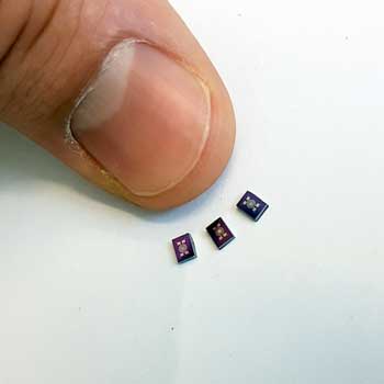
This is an image of the three gas sensors developed at ETH Zurich. (Image: ETH Zurich / Andreas Güntner)

Chemical „fingerprint”

As shown by laboratory tests in collaboration with Austrian and Cypriot scientists, this sensor combination can be quite useful when searching for entrapped people. The researchers used a test chamber at the University of Innsbruck’s Institute for Breath Research in Dornbirn as an entrapment simulator. Volunteers each remained in this chamber for two hours.
„The combination of sensors for various chemical compounds is important, because the individual substances could come from sources other than humans. CO2, for example, could come from either a buried person or a fire source,” explains Andreas Güntner, a postdoc in Pratsinis’ group and lead author of the study, published in the journal Analytical Chemistry („Sniffing Entrapped Humans with Sensor Arrays”). The combination of sensors provides the scientists with reliable indicators of the presence of people.

Suitable for inaccessible areas

The researchers also showed that there are differences between the compounds emitted via our breath and skin. „Acetone and isoprene are typical substances that we mostly breathe out. Ammonia, however, is usually emitted through the skin,” explains ETH professor Pratsinis. In the experiments in the entrapment simulator, the participants wore a breathing mask. In the first part of the experiment, the exhaled air was channelled directly out of the chamber; in the second part, it remained inside. This allowed the scientists to create separate breath and skin emission profiles.
The ETH scientists’ gas sensors are the size of a small computer chip. „They are about as sensitive as most ion mobility spectrometers, which cost thousands of Swiss francs and are the size of a suitcase,” says Pratsinis. „Our easy-to-handle sensor combination is by far the smallest and cheapest device that is sufficiently sensitive to detect entrapped people. In a next step, we would like to test it during real conditions, to see whether it is suited for use in searches after earthquakes or avalanches.”
While electronic devices are already in use during searches after earthquakes, these work with microphones and cameras. These only help to locate entrapped people who are capable of making themselves heard or are visible beneath ruins. The ETH scientists’ idea is to complement these resources with the chemical sensors.
They are currently looking for industry partners or investors to support the construction of a prototype. Drones and robots could also be equipped with the gas sensors, allowing difficult-to-reach or inaccessible areas to also be searched. Further potential applications could include detecting stowaways and exposing human trafficking.
Source: ETH Zurich

Microsensori cu sensibilitate ridicată la orizont(High-sensitivity microsensors on the horizon)

Microsensoarele wireless au permis noi modalități de a monitoriza mediul înconjurător, permițând utilizatorilor să măsoare spații care nu au depășit limitele cercetării, cum ar fi zone toxice, componente ale vehiculelor sau zone izolate din corpul uman.Explică modul în care noile dispozitive cu capacități mult mai mari decât cele ale senzorilor convenționali pot fi construite prin împrumutarea de concepte din mecanica cuantică.

Posted: May 14, 2018

High-sensitivity microsensors on the horizon

(Nanowerk News) Wireless microsensors have enabled new ways to monitor our environment by allowing users to measure spaces previously off limits to research, such as toxic areas, vehicle components, or remote areas in the human body. Researchers, however, have been stymied by limited improvements in the quality of data and sensitivity of these devices stemming from challenges associated with the environments they operate in and the need for sensors with extremely small footprints.

A new paper published today in Nature Electronics(„Generalized parity–time symmetry condition for enhanced sensor telemetry”) by researchers at the Advanced Science Research Center (ASRC) at The Graduate Center of The City University of New York, Wayne State University, and Michigan Technological University, explains how new devices with capabilities far beyond those of conventional sensors can be built by borrowing concepts from quantum mechanics.
parity-time symmetric electronic sensor for telemetry
Artistic rendering of a parity-time symmetric electronic sensor for telemetry. (Image: Pai-Yen Chen, Wayne State University)
The team, led by Andrea Alù, director of the ASRC’s Photonics Initiative and Einstein Professor of Physics at The Graduate Center, and Pai-Yen Chen, professor at Wayne State University, developed a new technique for designing microsensors that allows for significantly enhanced sensitivity and a very small footprint. Their method involves using isospectral parity-time-reciprocal scaling, or PTX symmetry, to design the electronic circuits. A ‘reader’ is paired with a passive microsensor that meets this PTX symmetry. The pair achieves highly sensitive radio-frequency readings.
„In the push to miniaturize the sensors to improve their resolution and enable large-scale networks of sensing devices, improving the sensitivity of microsensors is crucial,” Alù said. „Our approach addresses this need by introducing a generalized symmetry condition that enables high-quality readings in a miniaturized footprint.”
The work builds on recent advances in the area of quantum mechanics and optics, which have shown that systems symmetric under space and time inversion, or parity-time (PT) symmetric, may offer advantages for sensor design. The paper generalizes this property to a wider class of devices that satisfy a more general form of symmetry – PTX-symmetry. This type of symmetry, is particularly well-suited to maintain high sensitivity, while drastically reducing the footprint.
The researchers were able to show this phenomenon in a telemetric sensor system based on a radio-frequency electronic circuit, which exhibited drastically improved resolution and sensitivity compared to conventional sensors. The microelectromechanical (MEMS)-based wireless pressure sensors share the sensitivity advantages of previous PT-symmetric devices, but crucially the generalized symmetry condition allows both for device miniaturization and enables an efficient realization at low frequencies within a compact electronic circuit.
This new approach may allow researchers to overcome the current challenges in deploying ubiquitous networks of long-lasting, unobtrusive microsensors to monitor large areas. In the age of the internet of things and big data, such networks are useful for wireless health, smart cities, and cyber-physical systems that dynamically gather and store large amounts of information for eventual analysis.
„Development of wireless microsensors with high sensitivity is one of the major challenging issues for practical uses in bioimplants, wearable electronics, internet-of-things, and cyber-physical systems,” Chen said. „While there has been continuous progress in miniature micro-machined sensors, the basics of telemetric readout technique remains essentially unchanged since its invention. This new telemetry approach will make possible the long-sought goal of successfully detecting tiny physical or chemical actuation from contactless microsensors.”
Source: Advanced Science Research Center, GC/CUNY

Căptușeli MOF pentru a detecta gazele nocive(Lining MOF pockets to detect noxious gases)

Un material poros cu buzunare personalizate în structura sa este un material promițător pentru detectarea gazelor nocive. O peliculă subțire de material, acoperit pe un electrod, format un senzor electronic care ar putea detecta urme de dioxid de sulf gazos ( Journal of Materials Chemistry , „SO foarte sensibil și selectiv 2 senzor MF: integrarea MFM-300 MOF ca sensibil strat pe un electrod capsiv interdigitat ” ). Senzorul este un pas important către dispozitivele din lumea reală care pot străpunge gazele periculoase în aerul real.Cercetatorii au selectat o versiune pe baza de indiu a unui MOF numit MFM-300 ca material senzor.

Posted: May 03, 2018

Lining MOF pockets to detect noxious gases

(Nanowerk News) A porous material with tailor-made pockets stitched into its structure is a promising material for sensing noxious gases. A thin film of the material, coated onto an electrode, formed an electronic sensor that could detect traces of sulfur dioxide gas (Journal of Materials Chemistry, „Highly sensitive and selective SO2 MOF sensor: the integration of MFM-300 MOF as a sensitive layer on a capacitive interdigitated electrode”). The sensor is a significant step toward real-world devices that can sniff out dangerous gases in real air.

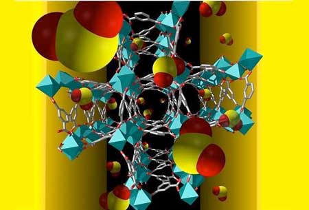
Sulfur dioxide molecules (red and yellow) are selectively taken up by pores in the metal-organic framework
Sulfur dioxide molecules (red and yellow) are selectively taken up by pores in the metal-organic framework. (Image: Valeriya Chernikova)
Although several lab-based analytical instruments can detect traces of a specific gas in the air, these instruments are typically large, expensive, power-hungry machines. There is still a need for small, inexpensive, energy-efficient sensors that, for example, could be widely deployed around industrial sites to continually monitor air quality.
One promising way to make such sensors involves porous materials called metal-organic frameworks (MOFs). By making the MOF from different metal atoms and organic linkers, researchers can create materials that selectively absorb specific gases into tailor-made pockets within the structure. Two King Abdullah University of Science and Technology (KAUST) research groups, led by materials scientist, Mohamed Eddaoudi, and electronic engineer, Khaled Salama, recently teamed up to develop MOF-based gas sensors.
The first step was completed in 2015 when the team made a proof-of-concept sensor by coating a MOF layer on to an electrode (Sensors, „Insights on Capacitive Interdigitated Electrodes Coated with MOF Thin Films: Humidity and VOCs Sensing as a Case Study”). The device senses gases in a similar way that a touchscreen senses a finger. The gas changes the MOF sensor’s capacitance, an electronic property that can be directly measured using the electrode.
Now, the team is working toward specific applications. “Our current work aims to identify the ideal MOF, in terms of sensitivity and selectivity, for detection of sulfur dioxide,” says Valeriya Chernikova, a Ph.D. student from Eddaoudi’s lab.
The researchers selected an indium-based version of a MOF called MFM-300 as their sensor material. A thin film of the material could be grown onto the electrode under mild conditions that do not damage the sensor circuit. The resulting material forms pockets lined with two -OH groups and four C-H groups that selectively bind sulfur-dioxide molecules. In lab tests using simple mixtures of gases, the sensor could detect sulfur dioxide at concentrations of just a few parts per billion.
To use the technology for real air—which comprises a much more complex mixture of gases—the next step is to develop sensor arrays that pool the responses of multiple MOF materials, Chernikova says. “The data will be processed using various statistical and machine learning algorithms to improve the accuracy of the sensor’s response,” she continues. “This is commonly referred to as an ‘artificial nose’.”
Source: King Abdullah University of Science and Technology

Membrana celulară inspiră un film electronic ultra-scurt(Cell membrane inspires new ultrathin electronic film)

Cercetatorii japonezi au dezvoltat o noua metoda de a construi arii mari de materiale semiconductoare, care are doar doua molecule groase si un total de 4.4 nanometri inaltime.Filmele funcționează ca tranzistori de film subțire și au aplicații potențiale viitoare în electronice flexibile sau detectoare chimice.Proprietățile semiconductoare ale bistratificatorului pot da aplicațiile de filme în electronică flexibilă sau în detectarea chimică.

Posted: May 03, 2018

Cell membrane inspires new ultrathin electronic film

(Nanowerk News) Japanese researchers have developed a new method to build large areas of semiconductive material that is just two molecules thick and a total of 4.4 nanometers tall (Advanced Materials, „Semiconductive single molecular bilayers realized using geometrical frustration”). The films function as thin film transistors, and have potential future applications in flexible electronics or chemical detectors. These thin film transistors are the first example of semiconductive single molecular bilayers created with liquid solution processing, a standard manufacturing process that minimizes costs.

3D computer model and Atomic Force Microscopy image of the new film made by University of Tokyo scientists
3D computer model and Atomic Force Microscopy image of the new film made by University of Tokyo scientists. Top surface view of 3D computer model (left) and Atomic Force Microscopy image (right) of the new film made by University of Tokyo scientists. The well-organized structure of the molecules is visible in both the 3D computer model and microscope image as a herringbone or cross-hair pattern. The color differences in the microscopy image are a result of the different lengths of the molecules’ tails; the length differences cause the geometric frustration that prevents layers from stacking. pm = picometers, nm = nanometers. (Image: Shunto Arai and Tatsuo Hasegawa)
„We want to give electronic devices the features of real cell membranes: flexible, strong, sensitive, and super thin. We found a novel way to design semiconductive single molecular bilayers that allows us to manufacture large surface areas, up to 100 square centimeters (39 square inches). They can function as high performance thin film transistors and could have many applications in the future,” said Assistant Professor Shunto Arai, the first author on the recent research publication.
Professor Tatsuo Hasegawa of the University of Tokyo Department of Applied Physics led the team that built the new film. The breakthrough responsible for their success is a concept called geometric frustration, which uses a molecular shape that makes it difficult for molecules to settle in multiple layers on top of each other.
The film is transparent, but the forces of attraction and repulsion between the molecules create an organized, repeated herringbone pattern when the film is viewed from above through a microscope. The overall molecular structure of the bilayer is highly stable. Researchers believe it should be possible to build the same structure out of different molecules with different functionalities.
Artist's representation of geometrically frustrated molecules
Artist’s representation of geometrically frustrated molecules. The molecules are aligned head-to-head (yellow portions) with their tails pointing in opposite directions (gray portions) so the molecules form a vertical line. The different tail lengths prevent additional layers of molecules from stacking on top. Thin film transistors made of single molecular bilayers will have better device performance than films that are irregular or greater thickness. (Image: The University of Tokyo)
The individual molecules used in the current film are divided into two regions: a head and a tail. The head of one molecule stacks on top of another, with their tails pointing in opposite directions so the molecules form a vertical line. These two molecules are surrounded by identical head-to-head pairs of molecules, which all together form a sandwich called a molecular bilayer.
Researchers discovered they could prevent additional bilayers from stacking on top by building the bilayer out of molecules with different length tails, so the surfaces of the bilayer are rough and naturally discourage stacking. This effect of different lengths is referred to as geometric frustration.
Standard methods of creating semiconductive molecular bilayers cannot control the thickness without causing cracks or an irregular surface. The geometric frustration of different length tails has allowed researchers to avoid these pitfalls and build a 10cm by 10cm (3.9 inches by 3.9 inches) square of their film using the common industrial method of solution processing.
Artist's representation of the blade coating solution process to produce single molecular bilayer thin film transistors
Artist’s representation of the blade coating solution process to produce single molecular bilayer thin film transistors. Liquid molecules are spread by a blade over the production surface at room temperature and standard air pressure in a technique called solution processing. As the liquid dries, the inter-molecular forces cause the molecules to automatically arrange themselves into geometrically frustrated single bilayers just 4.4 nanometers thick. (Image: Shunto Arai and Tatsuo Hasegawa)
The semiconductive properties of the bilayer may give the films applications in flexible electronics or chemical detection.
Semiconductors are able to switch between states that allow electricity to flow (conductors) and states that prevent electricity from flowing (insulators). This on-off switching is what allows transistors to quickly change displayed images, such as a picture on an LCD screen. The single molecular bilayer created by the UTokyo team is much faster than amorphous silicon thin film transistors, a common type of semiconductor currently used in electronics.
The team will continue to investigate the properties of geometrically frustrated single molecular bilayers and potential applications for chemical detection. Collaborators based at the National Institute of Advanced Industrial Science and Technology, the Nippon Kayaku Company Limited, Condensed Matter Research Center, and High Energy Accelerator Research Organization also contributed to the research.
Source: University of Tokyo

Disputa privind originea răspunsului foto terahertz în grafen are ca rezultat o remiză(The dispute about the origins of terahertz photoresponse in graphene results in a draw)

Aceste experimente vor ajuta la alegerea celui mai bun design pentru detectoarele terahertzi și ne vor aduce mai aproape de detectarea la distanță a substanțelor periculoase, diagnosticarea sigură medicală și comunicațiile wireless de mare viteză.

Posted: Apr 24, 2018

The dispute about the origins of terahertz photoresponse in graphene results in a draw

(Nanowerk News) Physicists at Moscow Institute of Physics and Technology (MIPT) and their British and Russian colleagues revealed the mechanisms leading to photocurrent in graphene under terahertz radiation. The paper published in Applied Physics Letters („Dual origin of room temperature sub-terahertz photoresponse in graphene field effect transistors”) not only puts a period to a long-lasting debate about the origins of direct current in graphene illuminated by high-frequency radiation but also sets the stage for the development of high-sensitivity terahertz detectors. Such detectors are highly demanded in medical diagnostics, wireless communications and security systems.

Photoresponse in graphene
Photoresponse in graphene. (Image: MIPT)
In 2005 MIPT alumni Andre Geim and Konstantin Novoselov experimentally studied the behavior of electrons in graphene, a flat honeycomb lattice of carbon atoms. They found that electrons in graphene respond to electromagnetic radiation with an energy of quantum, whereas the common semiconductors have an energy threshold below which the material does not respond to light at all. However, the direction of electron motion in graphene exposed to radiation has long remained a point of controversy, as there is a plenty of factors pulling it in different directions. The controversy was especially stark in the case of the photocurrent caused by terahertz radiation.
What sets terahertz radiation apart is its unique set of properties. As an example, it easily passes through many dielectrics without ionizing them: this is of particular value to medical diagnostic or security systems. A terahertz camera can „see” the weapons concealed under a person’s clothes, and a medical scanner can detect skin diseases at early stages by the spectral lines („fingerprints”) of characteristic biomolecules in the terahertz range. Finally, raising the carrier frequency of Wi-Fi devices from several to hundreds of gigahertz (into the sub-terahertz range) will proportionally increase the bandwidth. But all these applications need a sensitive and low-noise terahertz detector which is simple in fabrication.
Wiring diagram of a Graphene-based Terahertz Detector
Wiring diagram of a graphene-based terahertz detector: terahertz radiation hits the antenna connected to the left (source) and top (gate) terminals of a transistor. This generates direct photocurrent (or a constant voltage, depending on the measurement setup) between the left and right terminals, which is a measure of radiation intensity. (Image: MIPT)
A terahertz detector designed by researchers at MIPT, MSPU and the University of Manchester (the place where graphene was first discovered) is a graphene sheet (colored green in figures 1 and 2) sandwiched between dielectric layers of boron nitride and electrically coupled to a terahertz antenna–a metal spiral about a millimeter in size. As radiation impinges on the antenna, it rocks electrons on one side of the graphene sheet, while the resulting direct current is measured on the other side. It is the „packing” of graphene into boron nitride that enables record-high electric characteristics, giving the detector a sensitivity that is a cut above the earlier designs. However, the main result of the research is not a better-performing instrument; it is the insight into the physical phenomena responsible for the photocurrent.
There are three main effects leading to the electric current flowing in graphene exposed to terahertz radiation. The first one, the photothermoelectric effect, is due to the temperature difference between the antenna terminal and the sensing terminal. This sends electrons from the hot terminal to the cold one, like air rising up from a warm radiator up to cold ceiling. The second effect is the rectification of current at the terminals: it turns out that the edges of graphene let through only the high-frequency signal of a certain polarity. The third and most interesting effect is called plasma wave rectification. We can think of the antenna terminal as stirring up „waves in the electronic sea” of the graphene strip, while the sensing terminal registers the average current associated with these waves.
Operating Area of the Terahertz Detector
The operating area of the terahertz detector: the green strip is graphene, gold tracks lead to the antenna and a sensing ammeter. The scale bar is 6 microns. (Image: MIPT)
„Earlier attempts to explain the photocurrent in such detectors used only one of these mechanisms and excluded all the others,” says Dmitry Svintsov, head of the Laboratory of 2d Materials’ Optoelectronics at MIPT. „In reality, all three of them are at play, and our study found which effect dominates at which conditions. Thermoelectric effects dominate at low temperatures, while plasmonic rectification prevails at high temperatures and in longer-channel instruments. And the main thing is that we figured out how to make a detector in which the different photoresponse mechanisms will not cancel each other, but rather reinforce each other”
These experiments will help choose the best design for terahertz detectors and bring us closer to remote detection of dangerous substances, safe medical diagnostics, and high-speed wireless communications.
Source: Moscow Institute of Physics and Technology

Primul cip biosenzor din lume bazat pe cupru și oxid de grafen(World’s first biosensor chips based on copper and graphene oxide)

Cipurile pentru biosenzori sunt utilizate de companiile farmaceutice pentru a dezvolta medicamente. Aceste cipuri sunt, de asemenea, indispensabile pentru studierea cineticii interacțiunilor moleculare. Mai mult, ele ar putea servi drept bază pentru diferite tipuri de analizoare chimice utilizate pentru a găsi molecule care indică o boală și pentru a detecta substanțe periculoase în alimente sau în mediu, inclusiv scurgeri de la fabrici chimice, printre altele.

Posted: Apr 11, 2018

World’s first biosensor chips based on copper and graphene oxide

(Nanowerk News) Russian researchers from the Moscow Institute of Physics and Technology have developed biosensor chips of unprecedented sensitivity, which are based on copper instead of the conventionally used gold. Besides making the device somewhat cheaper, this innovation will facilitate the manufacturing process. The research findings are reported in the journal Langmuir(„Superior sensitivity of copper-based plasmonic biosensors”).

Biosensor chips are used by pharmaceutical companies to develop drugs. These chips are also indispensable for studying the kinetics of molecular interactions. Furthermore, they could serve as a basis for various kinds of chemical analyzers used to find molecules indicating a disease and to detect hazardous substances in food or the environment, including leaks from chemical plants, among other things.
The Russian research team from the Laboratory of Nanooptics and Plasmonics of MIPT’s Center for Photonics and 2D Materials has developed a sensing chip based on unconventional materials: copper and graphene oxide. As a result, their device achieves unmatched sensitivity, and yet its configuration is mostly standard and therefore compatible with existing commercial biosensors, e.g., such as Biacore, Reichert, BioNavis, or BiOptix.
Yury Stebunov, senior researcher at the Laboratory of Nanooptics and Plasmonics of the Center for Photonics and 2D Materials, MIPT
Yury Stebunov, senior researcher at the Laboratory of Nanooptics and Plasmonics of the Center for Photonics and 2D Materials, MIPT. (Image: Evgeniy Pelevin/MIPT)
“Our engineering solution is an important step towards developing biological sensors based on photonic and electronic technology,” says Valentyn Volkov, professor of the University of Southern Denmark, who also heads the Laboratory of Nanooptics and Plasmonics at MIPT. “By relying on standard manufacturing technologies and combining copper with graphene oxide — a material that has a great potential — we achieve a demonstrably high efficiency. This opens up new avenues for biosensor development.”
The most common material used in optoelectronics and photonics is gold. Nearly all commercial biosensor chips incorporate gold films several tens of nanometers thick — a nanometer is one billionths of a meter. The reason gold is so ubiquitous is that it has excellent optical properties and is chemically very stable. But even gold is not perfect. For one thing, it is expensive — specifically, high-purity gold costs over 25 times as much as high-purity copper. Also, gold is incompatible with the industrial processes used for manufacturing microelectronics, which severely limits its potential for application in device mass production.
Unlike gold, copper does not have these flaws. Its optical properties are on par with those of gold. Copper is used as an electrical conductor in microelectronics. However, it suffers from oxidation, or corrosion, and therefore has not been used in biochips. Now, MIPT researchers have solved this problem by covering the metal with a 10-nanometer dielectric layer. In addition to preventing oxidation, this altered the optical properties of the chip, making it more sensitive.
To further refine their biosensor design, the authors added a graphene oxide layer on top of the copper and dielectric films, enabling unprecedented sensitivity. This third material was originally obtained in 1859 as graphite oxide by Oxford University professor Benjamin C. Brodie Jr., a renowned English chemist. Later on, graphene oxide experienced a sort of a revival following the discovery of graphene — the first known two-dimensional material — by Russian-born University of Manchester physicists and MIPT graduates Andre Geim and Konstantin Novoselov. The work on graphene earned them the 2010 Nobel Prize in physics. Graphene oxide can be visualized as graphene — a one-dimensional sheet of carbon atoms bound in a honeycomb arrangement — with oxygen-containing groups dangling from some of the carbon atoms. These groups provide a link between the device surface and the protein molecules that are analyzed. In an earlier study, the authors used graphene oxide to increase the sensitivity of standard gold-based biosensors. The material proved to be beneficial for copper sensors as well.
Replacing gold with copper opens up the way for developing compact biosensing devices to be implemented in smartphones, portable gadgets, wearable devices, and smart clothes, because copper-based chips are compatible with conventional microelectronics technology. Scientists from across the world and electronics industry giants such as IBM and Samsung are putting a lot of effort into creating compact biosensors that could be built into electronic devices just like the present-day nano- and microelectromechanical motion sensors — accelerometers and gyroscopes. It is hard to overestimate the impact that biosensors would have — suffice to say that our devices would acquire a new sense organ. And this is not merely a metaphor: Major corporations are working on technologies to enable AI, intelligent gadgets, and biointerfaces that would serve as mediators between the human brain and a computer. A combination of these technologies could give rise to real cybernetic organisms.
“It is known that copper is susceptible to the corrosive influence of the environment. We have shown that protective dielectric films only tens of nanometers thick do more than just prevent oxidation: In some cases, they increase biosensor sensitivity,” says Yury Stebunov, the lead author of the paper and co-founder and CEO of GrapheneTek LLC. “We don’t see purely fundamental research as the final destination. Our solution will be available to potential customers before the end of the year. The technologies proposed in this study could be used to create miniature sensors and neural interfaces, and that’s what we’re working on right now.”
Source: Moscow Institute of Physics and Technology

Sentinel wrap: Un plasture transparent pentru detectarea pericolelor alimentare periculoase(Sentinel wrap: A transparent patch to detect dangerous food threats)

Un plasture transparent pentru detectarea pericolelor alimentare periculoase. dezvolta un plasture de testare transparent, tipărit cu molecule inofensive, care pot semnala contaminarea așa cum se întâmplă. Plasturele poate fi încorporat direct în ambalajul alimentar, unde poate monitoriza conținutul agenților patogeni nocivi precum E. coli și Salmonella.

Posted: Apr 06, 2018

Sentinel wrap: A transparent patch to detect dangerous food threats

(Nanowerk News) Is that meat still good? Are you sure? McMaster researchers have developed a test to bring certainty to the delicate but critical question of whether meat and other foods are safe to eat or need to be thrown out.

Mechanical and chemical engineers at McMaster, working closely with biochemists from across campus, have collaborated to develop a transparent test patch, printed with harmless molecules, that can signal contamination as it happens. The patch can be incorporated directly into food packaging, where it can monitor the contents for harmful pathogens such as E. coli and Salmonella.
Real-Time Monitoring of Food Contamination by Printing DNAzyme Probes on Food Packaging
The team has a transparent, durable, and flexible sensing surface that generates a fluorescence signal in the presence of a specific target bacterium. (© ACS)
The new technology, described in the research journal ACS Nano („Sentinel Wraps: Real-Time Monitoring of Food Contamination by Printing DNAzyme Probes on Food Packaging”), has the potential to replace the traditional „best before” date on food and drinks alike with a definitive indication that it’s time to chuck that roast or pour out that milk.
„In the future, if you go to a store and you want to be sure the meat you’re buying is safe at any point before you use it, you’ll have a much more reliable way than the expiration date,” says lead author Hanie Yousefi, a graduate student and research assistant in McMaster’s Faculty of Engineering.
If a pathogen is present in the food or drink inside the package, it would trigger a signal in the packaging that could be read by a smartphone or other simple device. The test itself does not affect the contents of the package.
According to the World Health Organization, foodborne pathogens result in approximately 600 million illnesses and 420,000 deaths per year. About 30 per cent of those cases involve children five years old and younger.
The researchers are naming the new material „Sentinel Wrap” in tribute to the McMaster-based Sentinel Bioactive Paper Network, an interdisciplinary research network that worked on paper-based detection systems. That network’s research ultimately gave rise to the new food-testing technology.
Chemical engineer Carlos Filipe and mechanical-biomedical engineer Tohid Didar, collaborated closely on the new detection project.
The signaling technology for the food test was developed in the McMaster labs of biochemist Yingfu Li.
„He created the key, and we have built a lock and a door to go with it,” says Filipe, who is Chair of McMaster’s Department of Chemical Engineering.
Mass producing such a patch would be fairly cheap and simple, the researchers say, as the DNA molecules that detect food pathogens can be printed onto the test material.
„A food manufacturer could easily incorporate this into its production process,” says Didar, an assistant professor of mechanical engineering and member of the McMaster Institute for Infectious Disease Research.
Getting the invention to market would need a commercial partner and regulatory approvals, the researchers say. They point out that the same technology could also be used in other applications, such as bandages to indicate if wounds are infected, or for wrapping surgical instruments to assure they are sterile.
Source: McMaster University

Minuscule, senzori montați pe dinți care pot urmări ce mănânci(Tiny, tooth-mounted sensors that can track what you eat)

Cu toate acestea, senzorul își poate schimba culoarea. De exemplu, în cazul în care stratul central primește sare sau etanol, proprietățile sale electrice se vor schimba, determinând senzorul să absoarbă și să transmită un spectru diferit de unde de radiofrecvență, cu o intensitate variabilă. Astfel pot fi detectate și măsurate substanțele nutritive și alți analit.
„Teoretic, putem modifica stratul bioresponsiv în acești senzori pentru a viza alte substanțe chimice

Posted: Mar 27, 2018
Tiny, tooth-mounted sensors that can track what you eat
(Nanowerk News) Monitoring in real time what happens in and around our bodies can be invaluable in the context of health care or clinical studies, but not so easy to do. That could soon change thanks to new, miniaturized sensors developed by researchers at the Tufts University School of Engineering that, when mounted directly on a tooth and communicating wirelessly with a mobile device, can transmit information on glucose, salt and alcohol intake.
In research to be published soon in the journal Advanced Materials („Functional, RF-trilayer sensors for tooth-mounted, wireless monitoring of the oral cavity and food consumption”), researchers note that future adaptations of these sensors could enable the detection and recording of a wide range of nutrients, chemicals and physiological states.
A miniaturized sensor mounted on a tooth
A miniaturized sensor mounted on a tooth. (Image: SilkLab, Tufts University)
Previous wearable devices for monitoring dietary intake suffered from limitations such as requiring the use of a mouth guard, bulky wiring, or necessitating frequent replacement as the sensors rapidly degraded. Tufts engineers sought a more adoptable technology and developed a sensor with a mere 2mm x 2mm footprint that can flexibly conform and bond to the irregular surface of a tooth. In a similar fashion to the way a toll is collected on a highway, the sensors transmit their data wirelessly in response to an incoming radiofrequency signal.
The sensors are made up of three sandwiched layers: a central “bioresponsive” layer that absorbs the nutrient or other chemicals to be detected, and outer layers consisting of two square-shaped gold rings. Together, the three layers act like a tiny antenna, collecting and transmitting waves in the radiofrequency spectrum. As an incoming wave hits the sensor, some of it is cancelled out and the rest transmitted back, just like a patch of blue paint absorbs redder wavelengths and reflects the blue back to our eyes.
The sensor, however, can change its “color.” For example, if the central layer takes on salt, or ethanol, its electrical properties will shift, causing the sensor to absorb and transmit a different spectrum of radiofrequency waves, with varying intensity. That is how nutrients and other analytes can be detected and measured.
“In theory we can modify the bioresponsive layer in these sensors to target other chemicals – we are really limited only by our creativity,” said Fiorenzo Omenetto, Ph.D., corresponding author and the Frank C. Doble Professor of Engineering at Tufts. “We have extended common RFID [radiofrequency ID] technology to a sensor package that can dynamically read and transmit information on its environment, whether it is affixed to a tooth, to skin, or any other surface.”
Source: Tufts University