Nanostructura pintenilor de urchin de mare inspiră un ciment mai bun(Nanostructure of the sea urchin spines inspires better cement)

a sintetizat cu succes cimentul la nano-nivel în conformitate cu acest principiu de „cărămidă și mortar”. În timpul acestui proces, au fost identificate macro-molecule care preluau funcția de mortar, fixând blocurile cristaline unul la celălalt pe scara nano, blocurile se asamblează într-un mod ordonat. Scopul este de a face cimentul mai durabil.Pe baza acestor calcule, cimentul optimizat a atins o valoare de 200 megapascali. Prin comparație: Cojile de mucegai, care sunt standardul de aur în rezistență la rupere, ajung la o valoare de 210 megapascali, care este doar puțin mai mare. Betonul utilizat în prezent în prezent are o valoare de două până la cinci megapascali

Posted: Nov 29, 2017

Nanostructure of the sea urchin spines inspires better cement

(Nanowerk News) The sea urchin spines are mostly made of calcite, usually a very brittle and fragile material. In the case of the sea urchin, however, the spines are much more durable than the raw material alone. The reason for its strength is the way that nature optimises materials using a brick wall-style architecture.

The research team Physical Chemistry, headed by Professor Helmut Cölfen, successfully synthesised cement at the nano-level according to this “brick and mortar principle”. During this process, macro-molecules were identified that take on the function of mortar, affixing the crystalline blocks to each other on the nano-scale, with the blocks assembling themselves in an ordered manner. The aim is to make cement more durable.
The study’s results are published in the 1 December 2017 issue of Science Advances(„Mesocrystalline calcium silicate hydrate: A bioinspired route toward elastic concrete materials”).
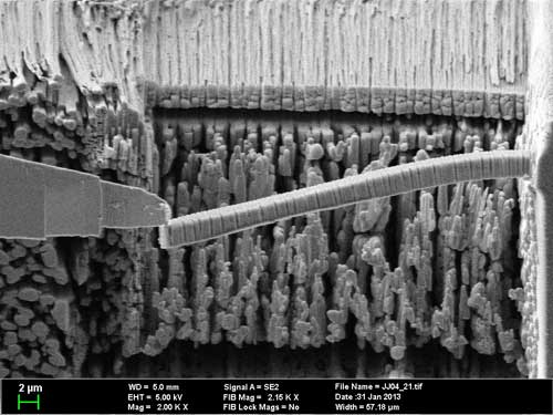
ending experiment on elastic cement in a scanning electron microscope
Bending experiment on elastic cement in a scanning electron microscope, enlarged 2,000 times Bar-shaped micro-structure precision-cut from nano-structured cement using an ion beam, bends under the pressure of a micro-manipulator without breaking (micro-manipulator left in the picture). (Image: Dr Zhaklina Burkhard)
“Our cement, which is significantly more fracture-resistant than anything that has been developed thus far, provides us with completely new construction possibilities”, Cölfen adds. A pillar made of this cement could be built 8,000 metres high, or ten times as high as the current tallest building in the world, before the material at its base would be destroyed by its weight. Normal steel, which has a value of 250 megapascals, could only reach 3,000 metres in height.
In nanoscience, brick wall-style architecture can be compared to the work of a mason: each layer of brick that is laid is held in place by mortar. The guiding principle is to layer hard, then soft, hard, then soft materials. This is exactly the principle nature uses to make sea urchin spines so resilient. When force is applied to the brittle calcite, its crystalline block does crack, however, the energy is then transferred to a soft disordered layer. Since this material has no cleavage planes to tear, it prevents further cracking. A thin section of sea urchin spine reveals this structural principle: crystalline blocks in an orderly structure are surrounded by a softer amorphous area. In the sea urchin’s case, this material is calcium carbonate.
Mussel shells or bones are constructed in much the same way. “Our goal is to learn from nature”, says Helmut Cölfen. The researcher has been honoured numerous times for his trailblazing results in the field of crystallisation, with, for example, the 2013 Academy Prize from the Berlin-Brandenburg Academy of Sciences and Humanities. Bionics or biomimetics is the term used for employing natural phenomena to inspire technical developments.
Cement itself has a disordered structure – each component sticks to all the others. This means: in order for cement to truly profit from the increased stability provided by brick and mortar construction, its structure will have to be reorganised at the nano-level. Helmut Cölfen describes the process as “encoding fracture-resistance at the nano-level”. In this case, it means identifying a material that bonds only with cement nanoparticles and nothing else in the cement. About ten negatively charged peptide combinations were identified that both adhere to and bond materials well.
In collaboration with the University of Stuttgart, the team was able to use an ion beam under an electron microscope to cut a bar-shaped micro-structure out of the nanostructured cement that was three micrometers in size. This micro-structure was then bent using a micro-manipulator. As soon as it was released, the micro-structure returned to its original position. Mechanical values could be calculated based on the elastic deformation of the micro-structure.
Based on these calculations, the optimised cement achieved a value of 200 megapascals. By comparison: Mussel shells, which are the gold standard in fracture-resistance, reach a value of 210 megapascals, which is only slightly higher. The concrete commonly used today has a value of two to five megapascals.
See urchin spines and mussel shells are made of calcite, because large quantities of calcium are available in water. Helmut Cölfen explains: “People have much better construction materials than calcite. If we succeed in designing the structures of materials and reproduce nature’s blueprints, we will also be able to produce much more fracture-resistant materials – high-performance materials inspired by nature”.
Source: Universität Konstanz

Producerea energiei termoelectrice la temperatura camerei: În curând?(Thermoelectric power generation at room temperature: Coming soon?)

Recent, cercetătorii de la Universitatea Osaka, în colaborare cu Hitachi, Ltd., au dezvoltat un nou material TE cu un factor de putere îmbunătățit la temperatura camerei. Studiul lor, publicat în Physica Status Solidi RRL ( „YtSi 2″ ): un material termoelectric promițător cu un factor de putere ridicat la temperatura camerei ” , ar putea ajuta aceste materiale să iasă din nișa la temperaturi înalte și în curentul principal.

Posted: Dec 26, 2017

Thermoelectric power generation at room temperature: Coming soon?

(Nanowerk News) Thermoelectric (TE) materials could play a key role in future technologies. Although the applications of these remarkable compounds have long been explored, they are mostly limited to high-temperature devices.

Recently, researchers at Osaka University, in collaboration with Hitachi, Ltd., developed a new TE material with an improved power factor at room temperature. Their study, published in Physica Status Solidi RRL („Ytterbium silicide (YbSi2): A promising thermoelectric material with a high power factor at room temperature”), could help bring these materials out of the high-temperature niche and into the mainstream.
Three-dimensional crystal structure of YbSi2
Fig.1. (a) Three-dimensional crystal structure of YbSi2, (b) view along the a-axis, and (c) along the c-axis.
TE materials display the thermoelectric effect: apply heat on one side, and an electric current starts to flow. Conversely, run an external current through the device, and a temperature gradient forms; i.e., one side becomes hotter than the other. By interconverting heat and electricity, TE materials can be used as either power generators (given a heat source) or refrigerators (given a power supply).
The ideal TE material combines high electrical conductivity, allowing the current to flow, with low thermal conductivity, which prevents the temperature gradient from evening out. The power generation performance mainly depends on the “power factor,” which is proportional to both electrical conductivity and a term called the Seebeck coefficient.
“Unfortunately, most TE materials are often based on rare or toxic elements,” according to study co-author Sora-at Tanusilp. “To address this, we combined silicon – which is common in TE materials – with ytterbium, to create ytterbium silicide (YbSi2). We chose ytterbium over other metals for several reasons. First, its compounds are good electrical conductors. Second, YbSi2 is non-toxic. Moreover, this compound has a specific property called valence fluctuation that make it a good TE material at low temperatures.”
Temperature dependences of (a) the Seebeck coefficient S, (b) electrical conductivity ?, (c) power factor S2? for YbSi2
Fig.2. Temperature dependences of (a) the Seebeck coefficient S, (b) electrical conductivity σ, (c) power factor S2σ for YbSi2. The reported data for Bi2Te3-based alloy are shown as solid lines for comparison. (click on image to enlarge)
The first advantage of YbSi2 is that the Yb atoms occupy a mixture of valence states, both +2 and +3. This fluctuation, also known as Kondo resonance, increases the Seebeck coefficient with keeping metal-like high electrical conductivity at low temperature, and therefore the power factor.
Second, YbSi2 has an unusual layered structure. While the Yb atoms occupy crystal planes similar to pure Yb metal, the Si atoms form hexagonal sheets between those planes, resembling the carbon sheets in graphite. This blocks the conduction of heat through the material, and therefore keeps the thermal conductivity down, preserving the temperature gradient. The researchers believe that heat conduction is further suppressed by controlling the structure in nanoscale and traces of impurities and other defects.
The result is an encouragingly high power factor of 2.2 mWm-1K-2 at room temperature. This is competitive with conventional TE materials based on bismuth telluride.
As corresponding author of this study Ken Kurosaki explains, “The use of Yb shows we can reconcile the conflicting needs of TE materials through carefully selecting the right metals. Room-temperature TEs, with moderate power, can be seen as complementary to the conventional high-temperature, high-power devices. This could help unlock the benefits of TE in everyday technology.”
Source: Osaka University

Camerele solare lavabile(Washable solar cells)

„fotovoltaice organice elastice acoperite cu elastomer rezistent la apă și etanșă pentru aplicații electronice lavabile” ). Noile celule fotovoltaice organice, ultrathine pot fi întinse la jumătatea lungimii lor și pot rezista la 20 de cicluri de spălare simulate.
Posibilitățile sunt tantalizante. Aceste proprietăți înseamnă că celulele ar putea fi încorporate, de exemplu, în dispozitivele textile și în dispozitivele Internet-of-Things (dispozitive în rețea care pot „vorbi” unul cu celălalt) pentru a crea îmbrăcăminte generatoare de energie electrică; power monitors personal health; și reîncărcați dispozitive mobile în mișcare.

Posted: Dec 22, 2017

Washable solar cells

(Nanowerk News) Hard, flat solar panels are hardly something most people want to wear against their skin. However, flexible, washable solar cells are on the horizon thanks to a recent breakthrough by a team at RIKEN led by Takao Someya (Nature Energy, „Stretchable and waterproof elastomer-coated organic photovoltaics for washable electronic textile applications”). The new organic, ultrathin photovoltaic cells can be stretched by half their length and withstand 20 simulated washing cycles.

The possibilities are tantalizing. These properties mean the cells could, for example, be incorporated into textiles and Internet-of-Things devices (networked devices that can ‘talk’ to each other) to create electricity-generating clothing; power personal health monitors; and recharge mobile devices on the go.
A photograph showing the ultrathin organic solar cell being washed and stretched
A photograph showing the ultrathin organic solar cell being washed and stretched. (Image: RIKEN)

An accordion in an elastomer sandwich

This is the first time that a single solar cell has combined a high energy efficiency, stretchabil­ity, and stability in air and water, explains lead researcher Kenjiro Fukuda from the Thin-Film Device Laboratory (Chief Scientist Laboratory) and the RIKEN Center for Emergent Matter Science (CEMS).
The work began, he says, when Kazuo Takimiya’s group at CEMS developed the solar cell’s ultrathin organic active layer, an organic photovoltaic (OPV). The layer converts sunlight into electricity at an efficiency of nearly 8 per cent, while also being very stable in air and water. Thicker OPVs can claim a peak conversion of 10 per cent—but for a photovoltaic material that is only 1 micrometer thick, 8 per cent is very high. And since the active material is very thin and based on an organic material, it can flex without breaking.
But the first solar cells produced with this active layer were not stretchable and were easily scratched. Fukuda’s group solved these issues by placing stretched rubber-like elastomer films over the outside. “First, we pre-stretch the elastomer and fix the ultrathin solar cells gently,” says Fukuda. “Next, the second elastomer is pre-stretched and attached, and we achieve this kind of sandwich structure.” When the elastomer films were allowed to relax, the embedded solar cell folded itself into an accordion-like structure with troughs and peaks.
This folded structure gives the cell its stretchability—when it is pulled, the folds flatten out, meaning the device can be extended up to half its length without damage.
The elastomer films also somewhat water­proofed the cells making them washable— something that the researchers tested by subjecting the cells to 20 cycles of mechanical compression while exposing them to water for one hour and 40 minutes. The cell’s efficiency dropped by only 20 per cent after this process.

Stretchy batteries needed

The hope is that these solar cells could power electronic devices such as sensors to measure a wearer’s heart rate, body temperature, blood pressure and other important medical parame­ters. They could also allow doctors to more easily monitor an out-patient’s condition as well as enable athletes to continually measure their per­formance. “Recently, smart sensors that monitor the heartbeat, pressure or electrodermal activity, have been attracting attention,” says Fukuda. “So there are now a lot of textiles with sensors embedded. By combining these technologies with our solar cells, we could achieve some very smart sensor clothes systems.”
Making a solar cell stretchable
Making a solar cell stretchable. (Image: RIKEN)
In the future, if sufficiently high voltages and currents can be realized, solar cells in clothing could also be used to recharge mobile devices and may even be able to supply household electricity, meaning things like OPV awnings could be used in, for example, developing regions.
And if the solar cells could be combined with thin, lightweight batteries, their usefulness could be enhanced even further. “We need a very thin or stretchable battery system, but this very difficult to realize,” says Fukuda. “Batteries need some thickness to store a lot of power.” But he adds: “If we can find a suitable collaborator, we could realize good synergy between our team and a battery research group.”

Commercializing the technology

Currently, OPV models cannot compete against traditional inorganic solar cells for longevity and therefore price. Rooftop models target lifetimes of 20 years, while organic photovoltaic cells are targeting lifetimes of less than 10 years for glass-based products and less than five years for flexible products. German researchers Ning Li and Christoph J. Brabec noted this in a commen­tary piece on RIKEN’s OPVs for Nature Energy.
But Brabec, who is from the Department of Material Science at Germany’s Friedrich-Alex­ander University Erlangen-Nürnberg, says: “We got excited about [Someya and Fukuda’s] work as it fits excellently into what we suggest as the roadmap for OPVs….[We] believe that OPVs should concentrate on integrated applications.”
“Integration into bags, glasses, etc. has been around for quite some time, but integration into textiles hasn’t been possible because OPVs couldn’t be washed.”
Fukuda says that real-world practical applications are probably three to five years down the track, but already there has been interest from companies in commercializing the technology.
The two main hurdles that will need to be overcome are the cost and size of the solar cells. The cells are currently limited to 10 centimeters by 10 centimeters and are fairly expensive to fabricate. But this is mostly down to the cost of the active layer, says Fukuda. The film coating, he says, is actually very thin and will ultimately reduce costs. “If companies commercialize this technology, they could develop a way to mass-produce the active layer material and reduce the cost.”
“Many companies are interested in our technology and have contacted us recently,” he says. “Collaborating with a company will accelerate commercialization.”
Fukuda and his team are currently working on improving the cells’ stability in air and stretchability.
Source: RIKEN

Un act de echilibrare catalitică(A catalytic balancing act)

Creând mai întâi un aliaj de două dintre cele mai dense elemente naturale și apoi eliminând unul, oamenii de știință au remodelat structura materialului rămas astfel încât să echilibreze mai bine trei factori importanți pentru reacțiile chimice: activitate, stabilitate și conductivitate.
„Găsirea unui material care să funcționeze bine pentru conversia sau stocarea energiei este ca și cum ai crea o căsnicie fericită”, a declarat Nenad Markovic, un cercetător în domeniul materialelor Argonne și autor al studiului. „În cazul nostru, am constatat că un parteneriat dinamic între două materiale diferite ne-a ajutat să integrăm preocupările concurente”.În condiții de funcționare, catalizatorul poros formează de fapt o carcasă unică de oxid de iridiu mai puțin conductiv în jurul interiorului metalic de iridiu foarte conductiv. În acest fel, electronii se pot mișca ușor prin cea mai mare parte a catalizatorului pentru a ajunge la suprafață, unde molecula de apă așteaptă pe electroni să inițieze reacția de divizare a apei.

Posted: Dec 22, 2017

A catalytic balancing act

(Nanowerk News) Balance forms the foundation for a happy life or a healthy diet. For scientists working to design new catalysts to create renewable energy, balancing different materials and their properties is equally important. (Catalysts help accelerate chemical reactions.)

In a new study (Nature Communications, „Balancing activity, stability and conductivity of nanoporous core-shell iridium/iridium oxide oxygen evolution catalysts”), researchers from the U.S. Department of Energy’s (DOE) Argonne National Laboratory, Johns Hopkins University, Drexel University and several universities in South Korea used a new and counterintuitive approach to create a better catalyst that supports one of the reactions involved in splitting water into hydrogen and oxygen. Scientists plan to use the generated hydrogen as a clean fuel.
By first creating an alloy of two of the densest naturally occurring elements and then removing one, the scientists reshaped the remaining material’s structure so that it better balanced three factors important for chemical reactions: activity, stability and conductivity.
“Finding a material that works well for energy conversion or storage is like creating a happy marriage,” said Nenad Markovic, an Argonne materials scientist and author of the study. “In our case, we found that a dynamic partnership between two different materials helped us integrate competing concerns.”
Scientists searching for new catalysts have scoured the periodic table to find the right elements or combinations of elements to maximize a catalyst’s activity in water-splitting reactions, as well as the durability of the active sites on its surface. Finding materials that are both stable and active, however, has been a challenge.
“More active catalysts tend to be less stable,” Markovic said. “Those that seem to work twice as well usually work only half as long. It is becoming obvious that designing active catalysts is not enough — we need to have not only active, but also stable, materials.”
For the new catalyst, Markovic and his colleagues turned to iridium, a metal most commonly associated with meteorites. As a thin film, iridium is catalytically active, but as it reacts over time with an electrolyte environment, iridium atoms become oxidized. During this process, some of them leave the catalyst’s surface through corrosion, increasingly impairing its performance.
The research team worked to prevent the oxidation by reorganizing the iridium’s structure. To help stabilize and activate iridium, they alloyed it with its neighbor on the periodic table, osmium.
Unlike iridium, osmium is neither catalytically active nor stable, but it did offer a key benefit. After alloying the osmium and iridium together, the researchers then de-alloyed the two metals, leaving behind only a reconfigured structure of three-dimensional iridium nanopores.
“Without the osmium, the iridium would never achieve this state,” Markovic said. “We needed to introduce and then remove the osmium to get a form of iridium that was both active and stable.”
Markovic said each nanopore’s enhanced catalytic stability is due to the small volume of electrolyte within a pore becoming quickly saturated with iridium ions so that surface atoms stop dissolving, in much the same way that it is easier to saturate a teacup of water with sugar than a 10-gallon jug.
While the nanopore’s structure addressed the need for a stable, active catalyst, it was another facet of the iridium’s reconfiguration that helped boost the material’s electron conductivity. Under operational conditions, the porous catalyst actually forms a unique shell of less-conductive iridium oxide around its highly conductive iridium metal interior. This way, electrons can move easily through most of the catalyst to reach the surface, where the water molecule waits on electrons to initiate the water-splitting reaction.
“Essentially, we’re trying to find a way to send electrons through on the ‘expressway,’ rather than making them take the side roads,” Markovic said. “This core-shell configuration [of the nanoporous material] allows us to do that.”
Source: Argonne National Laboratory

„Grafenă 3D” netedă „(Electronically-smooth ‘3D graphene’)

Cercetătorii au descoperit că materialul topologic bismutură trisodică (Na 3 Bi) poate fi fabricat ca fiind „electronic neted” ca alternativa bazată pe grafen cu cea mai bună calitate, menținând în același timp mobilitatea ridicată a electronilor grafenului.
Na 3 Bi este un Semimetal Dirac Topologic (TDS), considerat un echivalent 3D al grafenului prin aceea că arată aceeași mobilitate extraordinar de mare a electronilor.

Posted: Dec 22, 2017

Electronically-smooth ‘3D graphene’

(Nanowerk News) Researchers have found that the topological material trisodium bismuthide (Na3Bi) can be manufactured to be as ‘electronically smooth’ as the highest-quality graphene-based alternative, while maintaining graphene’s high electron mobility.

Na3Bi is a Topological Dirac Semimetal (TDS), considered a 3D equivalent of graphene in that it shows the same extraordinarily high electron mobility.
In graphene, as in a TDS, electrons move at constant velocity, independent of their energy.
This high electron mobility is highly desirable in materials investigated for fast-switching electronics. The flow of electrons in graphene can be, theoretically, 100 times as fast as in silicon.
However in practice there are limitations to graphene’s remarkable electron mobility, driven by the material’s two-dimensional nature.
Although graphene itself can be extremely pure, it is far too flimsy to use as a standalone material, and must be bound with another material. And because graphene is atomically thin, impurities in that substrate are able to cause electronic disorder within the graphene.
Such microscopic inhomogeneities, known as ‘charge puddles’, limit the mobility of charge carriers.
In practice, this means that graphene-based devices must be painstakingly constructed with a graphene sheet laid upon a substrate material that minimises such electronic disorder. Hexagonal boron-nitride (h-BN) is commonly used for this purpose.
But now, researchers at Australia’s FLEET research centre have found that trisodium bismuthide (Na3Bi) grown in their labs at Monash University are as electronically smooth as the highest-quality graphene/h-BN.
It’s a significant achievement, says lead researcher Dr Mark Edmonds. „This is the first time a 3D Dirac material has been measured in such a way,” Dr Edmonds says. „And we are excited to have found such a high degree of electronic smoothness in this material.”
The discovery will be critical for advancement of the study of this new topological material, which could have wide applications in electronics. „It’s impossible to know how many fields of research this could open,” says Dr Edmonds. „The same finding in graphene/h-BN sparked considerable supplementary studies in 2011.”
With electronic-smoothness of Na3Bi now demonstrated, an array of other research possibilities open up. There have been many studies into the relativistic (high mobility) flow of electrons in graphene since it was discovered in 2004. With this latest study, similar studies into Na3Bi can be expected.
Na3Bi offers a number of interesting advantages over graphene.
As well as avoiding the difficult construction methods involved in bi-layer graphene/h-BN devices, Na3Bi can be grown on a millimetre scale or larger. Currently, graphene-h-BN is limited to only a few micrometres.
Another significant advantage is the potential to use Na3Bi as the conducting channel in a new generation of transistors – one built upon the science of topological insulators. The study was published in Science Advances in December 2017 („Spatial charge inhomogeneity and defect states in topological Dirac semimetal thin films of Na3Bi”).

Next steps & topological transistors

„The discovery of electronically-smooth, thin films of TDS are an important step towards switchable topological transistors,” says FLEET Director Prof Michael Fuhrer.
„Graphene is a fantastic conductor, but it can’t be ‘switched off’, or controlled,” says Prof Fuhrer. „Topological materials, such as Na3Bi, can be switched from conventional insulator to topological insulator by the application of voltage or magnetic field.”
Topological insulators are novel materials that behave as electrical insulators in their interior, but can carry a current along their edges. Unlike a conventional electrical path, such topological edge paths can carry electrical current with near-zero dissipation of energy, meaning that topological transistors can switch without burning energy.
Topological materials were recognised in last year’s Nobel Prize in Physics.
Topological transistors would ‘switch’, just as a traditional transistor. The application of a gate potential would switch the edge paths in a Na3Bi channel between being a topological insulator (‘on’) and a conventional insulator (‘off’).

The bigger picture: energy use in computation

The overarching challenge is the growing amount of energy used in computation and information technology (IT).
Each time a transistor switches, a tiny amount of energy is burnt, and with trillions of transistors switching billions of times per second, this energy adds up. Already, the energy burnt in computation accounts for 5 per cent of global electricity use, and it’s doubling every decade.
For many years, the energy demands of an exponentially growing number of computations was kept in check by ever-more efficient, and ever-more compact computer chips – an effect related to Moore’s Law. But as fundamental physics limits are approached, Moore’s Law is ending, and there are limited future efficiencies to be found.
„For computation to continue to grow, to keep up with changing demands, we need more-efficient electronics,” says Prof Michael Fuhrer. „We need a new type of transistor that burns less energy when it switches.”
„This discovery could be a step in the direction of topological transistors that transform the world of computation.”
Source: ARC Centre of Excellence in Future Low-Energy Electronics Technologies
Subscribe to a free copy of one of our daily
Nanowerk Newsletter Email Digests
with a compilation of all of the day’s news.

Caracterizarea noului material compozit bazat pe foile de palmier date și deșeurile din polistiren expandat(

Testele de caracterizare termică a LPC au arătat și o conductivitate termică medie cuprinsă între 0,11 și 0,16 W / m · K. LPC poate fi utilizat în domeniul construcțiilor de construcții ca o bună izolare termică, precum și o componentă structurală în structurile sandwich. Mai mult, materialul LPC este obținut din deșeuri și poate fi reciclat în întregime la sfârșitul duratei sale de utilizare.

https://doi.org/10.1016/j.conbuildmat.2017.12.197

Caracterizarea noului material compozit bazat pe foile de palmier date și deșeurile din polistiren expandat

În scopul protecției mediului și valorificării resurselor vegetale, se efectuează un studiu experimental privind un material inovativ din lemn-plastic compozit (WPC) bazat pe date Palm și polistiren expandat, EPS, deșeuri. Data de deșeuri de folii de palmier sunt folosite ca armături, iar deșeurile EPS dizolvate în benzină sunt utilizate ca matrice. S-au considerat mai multe combinații de mărimi de întărire (0,1-0,315 mm, 0,315-0,5 mm și 0,5-1 mm) și raporturi de greutate fibră-matrice (70, 75 și 80% în greutate) pentru a investiga proprietățile compozitului de foițe-polistiren (LPC). În acest studiu s-au efectuat caracterizări fizice, mecanice, termice și morfologice pentru a determina: densitatea în vrac, modulul de flexiune, tensiunea maximă și conductivitatea termică a LPC. Prin urmare, măsurarea densității Pycnometer, testul de îndoire în trei puncte s-a efectuat și s-a folosit metoda sursă de căldură plană tranzitorie (hotdisc). Mai mult, o caracterizare prin microscopie electronică de scanare (SEM) a fost realizată pentru a observa legătura fibrelor / matricei. LPC a demonstrat o bună stare de adeziune a interfeței matrice-fibră și a unor proprietăți mecanice acceptabile, cu un modul de flexiune și un efort maxim care poate atinge 0,78 GPa și respectiv 2,84 MPa. LPC are o densitate cuprinsă între 542 și 824 kg / m3 care sunt comparabile cu cele ale materialelor obișnuite, cum ar fi lemnul tare și moale, MDF și alte tipuri de pulbere de sticlă WPC găsite în literatură. Testele de caracterizare termică a LPC au arătat și o conductivitate termică medie cuprinsă între 0,11 și 0,16 W / m · K. LPC poate fi utilizat în domeniul construcțiilor de construcții ca o bună izolare termică, precum și o componentă structurală în structurile sandwich. Mai mult, materialul LPC este obținut din deșeuri și poate fi reciclat în întregime la sfârșitul duratei sale de utilizare.

Tricoul cuantic blochează fundalul „chatter” în dispozitivele de detectare(Quantum trick blocks background ‘chatter’ in sensing devices)

Acestea ar putea fi folosite și în sistemele de apărare și securitate care utilizează magnetometre cuantice îmbunătățite, dispozitive care măsoară modificările câmpurilor magnetice pentru identificarea și urmărirea țintă.

Posted: Dec 19, 2017

Quantum trick blocks background ‘chatter’ in sensing devices

(Nanowerk News) A University of Sydney team has solved a common problem in quantum sensing devices, which are used in biomedical imaging and have defence applications.

Industrial sensors are everywhere in our technology and in order to function successfully they must be able to identify tiny signals from a cluttered background.
For most humans this is simple. Walk into a crowded room and you can pick out a single voice while ignoring everyone else. That trick isn’t so easy for industrial sensors – and the challenge gets even harder for super-sensitive quantum devices.
Now, a team led by Professor Michael J. Biercuk from the University of Sydney, in collaboration with Dartmouth College and Johns Hopkins Applied Physics Laboratory in the US, has developed quantum control techniques enabling a new generation of ultra-sensitive sensors that can identify tiny signals while rejecting background noise down to theoretical limits.
An Ion Trap Used to Confine Individual Atoms
An ion trap in Professor Michael J. Biercuk’s laboratory in the Sydney Nanoscience Hub. (Image: University of Sydney)
„By applying the right quantum controls to a qubit-based sensor, we can adjust its response in a way that guarantees the best possible exclusion of the background clutter – that is, the other voices in the room,” said Professor Biercuk, a chief investigator at the ARC Centre of Excellence for Engineered Quantum Systems.
While devices themselves have improved, the measurement protocols used to capture and interpret the signals have lagged behind. Quantum sensors therefore often return fuzzy results, which complicates interpretation of the data through a phenomenon known as „spectral leakage” – a bit like being distracted by the wrong voices in the room.
The University of Sydney research, published on Tuesday in Nature Communications („Application of optimal band-limited control protocols to quantum noise sensing”), demonstrates control protocols that will help take advantage of improved sensor hardware.
The experiments, using trapped atomic ions, have reduced spectral leakage by many orders of magnitude over conventional methods. Professor Biercuk said in certain circumstances, the methods they have developed are up to 100 million times better at excluding this background.
Six ytterbium Atoms
Six ytterbium atoms in an ion trap in Professor Michael J. Biercuk’s laboratory at the Sydney Nanoscience Hub. (Image: University of Sydney)
Quantum sensors take advantage of the very thing that makes building quantum computers so difficult. Quantum bits, or qubits, are the building blocks of quantum computers but they are highly prone to losing their quantum properties due to interference from the environment. This challenge can be turned on its head and used to build sensors that are much more responsive to the environment than classical technologies.
Professor Biercuk said the new protocols could have applications in medicine, such as imaging inside living cells using nanodiamonds. They could also be used in defence and security systems that use quantum-enhanced magnetometers, devices that measure changes in magnetic fields for target identification and tracking.
He said: „Our approach is relevant to nearly any quantum sensing application and can also be applied to quantum computing as it provides a way help identify sources of hardware error. This is a major advance in how we operate quantum sensors.”
Professor Biercuk has recently launched a venture-capital-backed spin-off from the work being done at the University of Sydney. Q-Ctrl aims to be the trusted provider of quantum control solutions for all new quantum technologies.
Source: University of Sydney

Microstructura adezivă în formă de perete biomimetic pentru atașarea indusă de forfecare(Biomimetic wall-shaped adhesive microstructure for shear-induced attachment)

efectele unghiului de tragere și deplasarea preliminară;Până în prezent, o mână de adezivi asemănători gecko-ului inspirat de firele de atașare în formă de spatula au fost sugerate pe baza geometriei pană și a clapetei elementelor de contact

Interface