Suprafețele rezistente la apă pot fi eficiente în apă, menținând răcirea electronică(Water-repellent surfaces can efficiently boil water, keep electronics cool)

Pre-udarea texturii unei suprafețe superhidrofobe duce la „fixarea” bulelor mici în timpul fierbei, ceea ce înseamnă că ele nu se întind pe suprafață în timp ce se extind. În schimb, ei se îndepărtează fără a coaliza într-o pătură de vapori și ajută la menținerea suprafeței umezite cu apă lichidă. Materialele hidrofobe pot, de asemenea, să formeze mult mai multe bule mici decât suprafețele hidrofile, permițând astfel răcirea mai eficientă a suprafeței.Suprafetele care resping apa pot sustine un punct de fierbere eficient daca tot aerul si vaporii sunt scosi dintr-un sistem

Posted: Apr 30, 2018

Water-repellent surfaces can efficiently boil water, keep electronics cool

(Nanowerk News) Surfaces that repel water can support efficient boiling if all air and vapor is removed from a system first, according to research featured on the cover of the most recent issue of Physical Review Letters („Enabling Highly Effective Boiling from Superhydrophobic Surfaces”).

Water is typically boiled off hydrophilic surfaces to cool nuclear reactors and high-power electronics, preventing them from overheating. Purdue University research has shown that the most water-repellent surfaces possible, superhydrophobic materials, not only can boil water efficiently under the right conditions, but also stay cooler than hydrophilic surfaces.
„One of the ways to take heat out of a surface is to boil from it,” said Justin Weibel, associate research professor of mechanical engineering. „But no one typically considers using superhydrophobic surfaces to improve boiling.”
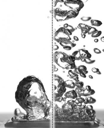
Boiling from a Water-Proof Surface
Superhydrophobic surfaces are normally insulated by vapor when brought to a boil (left), but getting water to stick makes them boil very efficiently (right), better than hydrophilic surfaces. (Image: Taylor Allred, Purdue University)
Consumer electronics – including laptops and even some smartphones – have water within metal „heat pipes” that dissipate the heat generated when these devices are in use, cooling them off. High-power electronics used in electric vehicles, supercomputers and aircraft particularly call for more efficient means to prevent overheating.
„Superhydrophobic surfaces were previously thought to be bad for boiling because they can’t stay wet,” said Taylor Allred, a Purdue doctoral student in mechanical engineering and first author on the paper. „You get a blanket of vapor on the surface, and because vapor is a very good insulator of heat, you are insulating the surface instead of cooling it.”
Past research has led scientists to believe that without this layer of insulating vapor, superhydrophobic surfaces could potentially boil at lower temperatures than hydrophilic ones. Several studies have attempted making patterned surfaces to get the benefits of both hydrophilic and hydrophobic materials, but researchers hadn’t yet achieved an entirely vapor-free surface with patterning due to the hydrophobic regions.
„We realized that if we could perform one key step prior to boiling from the superhydrophobic surface, we could get the best of both hydrophobic and hydrophilic surface behaviors all in one,” said Suresh Garimella, Purdue’s Goodson Distinguished Professor of Mechanical Engineering and director of the Cooling Technologies Research Center.
Allred first submerged the surface and then heated the surrounding water, being careful to not boil directly from the surface itself. Doing so removed the layer of air that is normally trapped within the texture of the superhydrophobic surface, allowing water to instead penetrate the texture and fully wet it as it would for a hydrophilic surface.
Pre-wetting the texture of a superhydrophobic surface results in the „pinning” of small bubbles during boiling, meaning that they don’t spread out over the surface as they expand. They instead depart without coalescing into a vapor blanket and help keep the surface wet with liquid water. Hydrophobic materials are also able to form many more small bubbles than hydrophilic surfaces, allowing the surface to be cooled more efficiently.
„There are numerous papers on making superhydrophobic surfaces and using them for a variety of applications. With this research, we’ve opened up a whole new area where they can be deployed,” Garimella said.
Source: Purdue University

Oamenii de știință creează nanomateriale care se reconfigurează ca răspuns la semnalele biochimice(Scientists create nanomaterials that reconfigure in response to biochemical signals)

O provocare majoră în domeniul științei materialelor este dezvoltarea de nanomateriale care pot replica aspecte ale acestor funcții celulare și se pot integra cu sistemele vii.dar ceea ce avem până acum este un progres interesant care demonstrează posibilitatea creării de materiale fabricate de om, care să imite o activitate complexă și dinamică a sistemelor biologice. Aceste noi nanomateriale au capacitatea de a răspunde la semnalele chimice relevante din punct de vedere biologic și oferă o interfață electronică.

Posted: Apr 30, 2018

Scientists create nanomaterials that reconfigure in response to biochemical signals

(Nanowerk News) Biological cells have the complex and miraculous ability to reconfigure and change the way they communicate with each other over time, allowing them to nimbly direct critical functions in the human body – from thinking to walking to fighting disease. A major challenge in materials science is developing nanomaterials that can replicate aspects of these cellular functions and integrate with living systems.

In a paper published in Nature Chemistry („Amino-acid-encoded biocatalytic self-assembly enables the formation of transient conducting nanostructures”), a team of researchers led by scientists at the Advanced Science Research Center (ASRC) at The Graduate Center of The City University of New York detail how they have created synthetic materials with the ability to mimic some behaviors normally associated with living matter.
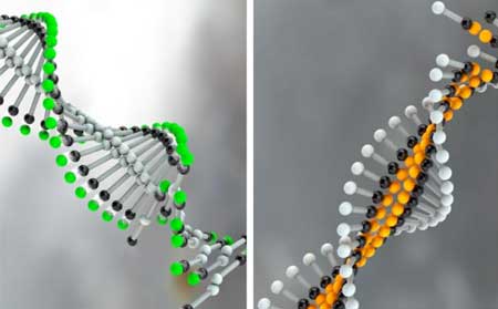
Formation of Electronic Nanowires
Formation of electronic nanowires is chemically programmed by incorporation of amino acids into self-assembling molecules. (Image: Ella Maru Studio)
„The ability to self-assemble, reconfigure and disassemble in response to chemical signals is a common trait in biological materials, but not in manmade ones” said Mohit Kumar, the paper’s lead author and a scientist with Rein Ulijn’s research group at the ASRC’s Nanoscience Initiative and Hunter College. „If you want to integrate synthetic materials into biology, a seamless interface is desirable, which requires materials that share some of the properties of living matter. Our approach will hopefully open the door to manmade materials that can interact with and repair living systems.”
To develop nanomaterials that reconfigure in response to chemical signals, researchers started with the base molecule naphthalenediimide (NDI), which is an organic semiconductor. The molecule was selectively modified on both sides by exposing it to biochemical signals in the form of simple amino acids that were added to the system. An enzyme was used to incorporate the amino acids onto the core molecule, triggering self-assembly and disassembly pathways. This process allowed the formation and degradation of nanomaterials with wire-like features capable of conducting electrical signals.
By using different amino acids, researchers were able to direct the development of nanomaterials with different properties, including a programmable nanostructure with the ability to turn electrical conduction on and off through the use of time-dependent self-assembly and disassembly.
„Like neurons in the brain, these materials exhibit a remarkable ability to remodel their electrical connections,” said Allon Hochbaum, a co-author of the paper and material scientist at the Samueli School of Engineering, University of California, Irvine (UCI). „The assembly of these molecules is encoded in their dynamic chemistry, so by simply changing the chemical inputs, we can observe insulating nanomaterials, conductive nanomaterials, or nanomaterials that dynamically switch between conducting and non-conducting states. The fact that their assembly and conductivity evolve in water makes these materials all the more compelling for bio-interfacing applications.”
Funding for the research was provided by the Air Force Office for Scientific Research and the Army Research Office. UCI researchers developed the devices for measuring the nanomaterials’ electrical conducting abilities, while ASRC researchers developed the nanomaterials. The collaborative team’s next step is to interface the new nanomaterials with actual neurons to see how the manmade and biological materials interact.
„We want to see if we can use the dynamic electro-conducting nanomaterials to effectively interface with neurons and result in their on-demand electrical firing,” said Rein Ulijn, director of the ASRC’s Nanoscience Initiative. „We’re still early in that aspect of the work, but what we have so far is an exciting breakthrough that demonstrates the possibility for creating manmade materials that mimic a complex, dynamic activity of biological systems. These new nanomaterials have the ability to respond to biologically relevant chemical signals and provide an electronic interface. In the long run, this may open up a new pathway towards developing treatments that, until now, have only been theoretical.”
Source: Advanced Science Research Center, GC/CUNY

Răsuciți grafenul în spirală(Twisting graphene into spirals)

Echipa a confirmat natura helicoidală a structurii prin cristalografie cu raze X, găsind și nanografi în sensul acelor de ceasornic și în sens invers acelor de ceasornic. Teste suplimentare au arătat că structura electronică și proprietățile de fotosabsorbție ale acestui compus sunt mult diferite de cele anterioare.

Posted: Apr 26, 2018

Twisting graphene into spirals

(Nanowerk News) Researchers from Kyoto University and Osaka University report for the first time in the Journal of the American Chemical Society („Hexa-peri-hexabenzo[7]helicene: Homogeneously -Extended Helicene as a Primary Substructure of Helically Twisted Chiral Graphenes”) the successful synthesis of hexa-peri-hexabenzo[7]helicene, or ‘helical nanographene’.

Schenmatic concept of nanographenes
Schenmatic concept of nanographenes. (Image: Osaka University and Kyoto University)
These graphene constructs previously existed only in theory, so successful synthesis offers promising applications from nanoscale induction coils, to molecular springs for use in nanomechanics.
Graphene – a hexagonal lattice of single layer carbon atoms exhibiting outstanding charge and heat transport properties – has garnered extensive research and development interest.
Helically twisted graphenes have a spiral shape. Successful synthesis of this type of graphene could have major applications, but its model compounds have never been reported. And while past research has gotten close, resulting compounds have never exhibited expected properties.
„We processed some basic chemical compounds through step-by-step reactions, such as McMurry coupling, followed by stepwise photocyclodehydrogenation and aromatization,” explains first author Yusuke Nakakuki. „We then found that we had synthesized the foundational backbone of helical graphene.”
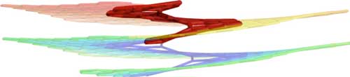
Chemical structure of  nanographene
Chemical structure of the nanographene synthesized in the present work. (Image: Osaka University and Kyoto University)
The team confirmed the helicoid nature of the structure through X-ray crystallography, also finding both clockwise and counter-clockwise nanographenes. Further tests showed that the electronic structure and photoabsorption properties of this compound are much different from previous ones.
„This helical nanographene is the first of its kind,” concludes lead author Kenji Matsuda. „We will try to expand their surface area and make the helices longer. I expect to find many new physical properties as well.”
Source: Osaka University

Inginerii dezvoltă o metodă nouă de rezolvare a texturii de spin a stărilor topologice de suprafață utilizând măsurători de transport(Engineers develop novel method for resolving spin texture of topological surface states using transport measurements)

Efectul de magneto-rezistență este tendința unui material de a schimba valoarea rezistenței sale electrice într-un câmp magnetic aplicat extern. Acesta a fost folosit pe scară largă pentru aplicații în senzori și capete de citire pe hard disk. Până în prezent, nu a fost stabilită nici o legătură între magnitorezistențele existente și textura spinării materialelor spin-polarizate. Cercetătorii de la Universitatea Națională din Singapore (NUS) au făcut recent un progres în acest domeniu, dezvăluind o strânsă legătură între textura de spin a stărilor de suprafață topologică (TSS) și un nou tip de rezistență la magneto.Rezultatele noastre pot fi aplicate la familii extinse de materiale foarte spin-polarizate, cum ar fi sistemele Rashba / Dresselhaus, precum si dichalcogenidele cu tranzitie bidimensionala cu stari spin-polarizate. De asemenea, oferă o nouă cale de detectare a texturii 3D a acestor materiale printr-o simplă măsurătoare de transport. „

Posted: Apr 26, 2018

Engineers develop novel method for resolving spin texture of topological surface states using transport measurements

(Nanowerk News) The magneto-resistance effect is the tendency of a material to change the value of its electrical resistance in an externally-applied magnetic field. It has been widely utilised for applications in sensors and hard disk reading heads. So far, no link has been established between the existing magneto-resistances and spin texture of spin-polarised materials. Researchers from the National University of Singapore (NUS) have recently made a breakthrough in this field, revealing a close relation between the spin texture of topological surface states (TSS) and a new kind of magneto-resistance.

This fundamental advancement is achieved in collaboration with researchers from the University of Missouri, United States. The research team observed for the first time a novel magneto-resistance in three-dimensional (3D) topological insulators (TIs), which scales linearly with both the applied electric and magnetic fields, and shows a close link to the in-plane and out-of-plane spin textures of TSS. The team’s finding could help in addressing the issue of spin current source selection often faced in the development of spintronic devices.
The research team, led by Associate Professor Yang Hyunsoo from the Department of Electrical and Computer Engineering at the NUS Faculty of Engineering, published their findings in the journal Nature Physics („Bilinear magnetoelectric resistance as a probe of three-dimensional spin texture in topological surface states”).
Bilinear magnetoelectric resistance as a probe of three-dimensional spin texture in topological surface states
(a) Schematic diagram illustrating the Dirac cone of a topological insulator. (b) Spin-momentum locked surface state with hexagonal warping. (c,d) Hall bar device of topological insulator Bi2Se3for harmonic resistance measurements. (e) Second harmonic resistance signal for the three scans of magnetic fields in xy, zy, and zx planes. (Image: NUS) (click on image to enlarge)

New magneto-resistance found in 3D TI

The discovery of 3D TIs has generated great interest among international researchers to understand the physical properties of this new state of matter, and exploring its applications in optoelectronics and spintronics. So far, the magneto-resistances found in 3D TIs is current-independent, reflecting a linear response of the electron transport to an applied electric field. At the same time, a transport obstacle exists in detecting the surface properties, due to the significant bulk contribution, which overwhelms the surface responses.
“In this work, we observed the second order nonlinear magneto-resistance in a prototypical 3D TI Bi2Se3 films, and showed that it is sensitive to TSS. In contrast with conventional magneto-resistances, this new magneto-resistance shows a linear dependence on both the applied electric and magnetic fields,” said Dr He Pan, who is the first author of the study and a Research Fellow at the Department.
Assoc Prof Yang added, “Theoretical calculations by our collaborators from the University of Missouri revealed that the bilinear magneto-electric resistance originates from the spin-momentum locked TSS with hexagonal warping. From the perspective of the microscopic origin, it is a fundamentally new process regarding the conversion of a nonlinear spin current into a charge current under the external magnetic field.”

Novel technique to probe 3D spin texture

Probing the surface spin texture is of critical importance for the development of TI-based spintronic devices. However, the approach performed to date is highly restricted to sophisticated tools such as photoemission spectroscopy.
The novel magneto-electric resistance observed by the research team provides a new route to detect the 3D spin texture in TSS by a simple electric transport measurement without involving any additional ferromagnetic layers. The team’s study also revealed the hexagonal warping effect in TSS, which could previously only be determined by photoemission spectroscopy.
Commenting on the significance of the breakthrough, Dr He Pan said, “Our results can be applied to extended families of highly spin-polarised materials, like Rashba/Dresselhaus systems as well as two-dimensional transition metal dichalcogenides with spin-polarised states. It also provides a new route to detect the 3D spin texture of these materials by a simple transport measurement.”

Next steps

Moving forward, Assoc Prof Yang and his team are conducting experiments to increase the magnitude of the novel magneto-resistance by refining the TI materials and film thickness. They are also planning to incorporate and test the technology in different materials. The team hopes to work with industry partners to explore various applications with the novel magneto-resistance.
Source: National University of Singapore

Găurirea găurilor în grafen pentru a stimula producția de hidrogen(Punching holes in graphene to boost hydrogen production)

au descoperit ca grafenul „holey” ofera o cale in jurul acestei probleme. Ei foloseau coli de grafen dopate cu azot pentru a încapsula un aliaj de electrozi de nichel-molibden (NiMo). Crucial, grafenul a fost perforat plin de găuri de dimensiuni nanometrice, ca un șuviță.

Posted: Apr 26, 2018

Punching holes in graphene to boost hydrogen production

(Nanowerk News) Researchers may have brought the renewable energy future one step closer. A new electrode can accomplish the hydrogen evolution reaction (HER) in acidic conditions, making the technology both cheaper and more effective. The process is helped by a smart form of graphene.

The electrolysis of water to hydrogen is vital for energy storage in a green economy. One of the major obstacles, however, is the high cost of noble-metal electrodes. Cheaper non-nobles do work, but mainly in alkaline conditions, where the reaction is electricity-hungry; the more efficient acid-phase reaction requires scarce commodity metals such as platinum. Worse still, the acid electrolytes are corrosive and eat away at the core metal.
Now, researchers led by the University of Tsukuba have found that “holey” graphene offers a way round this problem. They used nitrogen-doped graphene sheets to encapsulate a nickel–molybdenum (NiMo) electrode alloy. Crucially, the graphene was punched full of nanometer-size holes, like a colander.
In a study in ACS Catalysis („Cooperation between holey graphene and NiMo alloy for hydrogen evolution in an acidic electrolyte”), they showed that in acid conditions, the new HER system dramatically outperforms an electrode using regular non-holey graphene.
Porous NiMo composite covered with holy graphene
Porous NiMo composite covered with holy graphene. (Image: University of Tsukuba)
The use of graphene in HER electrodes is not new – this flexible, conductive carbon sheet is ideal for wrapping around the core metal. However, while protecting the metal against corrosion, graphene also suppresses its chemical activity. In the new Tsukuba system, the all-important holes promote the reaction in two ways, while the intact graphene part protects the metal.
“We created holes by decorating the NiMo surface with silica nanoparticles,” explains study co-author Kailong Hu. “Then, when we deposited the graphene layer, gaps were left behind at the nanoparticle positions – like a relief artwork. In fact, the holes are more than just gaps – they are ringed by chemically active ridges called ‘fringes’. Technically, these fringes are structural defects, but they drive the chemistry of the electrode.”
Compared with normal graphene, the fringes are more hydrophilic. This attracts hydronium (H3O+) in the acid solution, which plays a crucial role in one of the two HER mechanisms. The fringes are also excellent at adsorbing single H atoms, which provides extra surface area for the other important HER process. As a result, H2 is produced as efficiently as on a conventional (but expensive) Pt/C electrode. Meanwhile, the non-holey part of graphene delays the metal catalyst from dissolving in the acid.
“This is a versatile new concept for hydrogen evolution electrodes,” lead author Yoshikazu Ito says. “The goal is to minimize the overpotential needed for the reaction. Therefore, it’s not limited to one particular catalyst. We tuned our holey graphene layer specifically to NiMo by optimizing the size and number of holes. What’s impressive is that the catalyst was still stable in acid, despite the holes. In the future, holey graphene could be customized to a range of metals, pushing the efficiency of hydrogen production toward full-scale adoption.”
Source: University of Tsukuba

LALO Tactical Prototype Bloodbird și pantofi de pantofi cu camuflaj digital Camo (Camuflaj) Modelul țesut superior: o „greșeală fericită”(LALO Tactical Prototype Bloodbird and Grinder Sneakers with Digital Combat Camo (Camouflage) Pattern Woven Uppers: A ‘Happy Mistake’)

Defense Review va incerca sa obtina cateva pantofi adidasi LALO Tactical pentru a le testa pe sosea si la gama, cat mai curand posibil. Ne-ar plăcea foarte mult să obținem cel puțin o pereche pe scriitorul / contribuitorul DR și pe pictorul lui Jeff Gurwitch, șeful noului produs. Deci, fii atent la o revizuire de la noi.

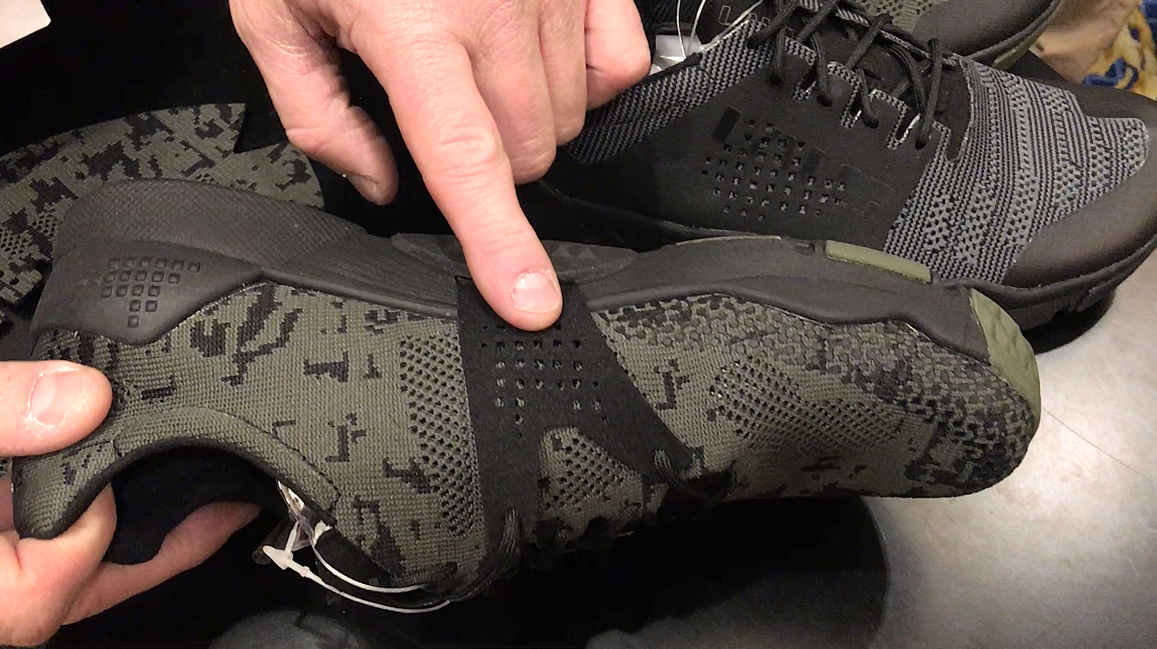
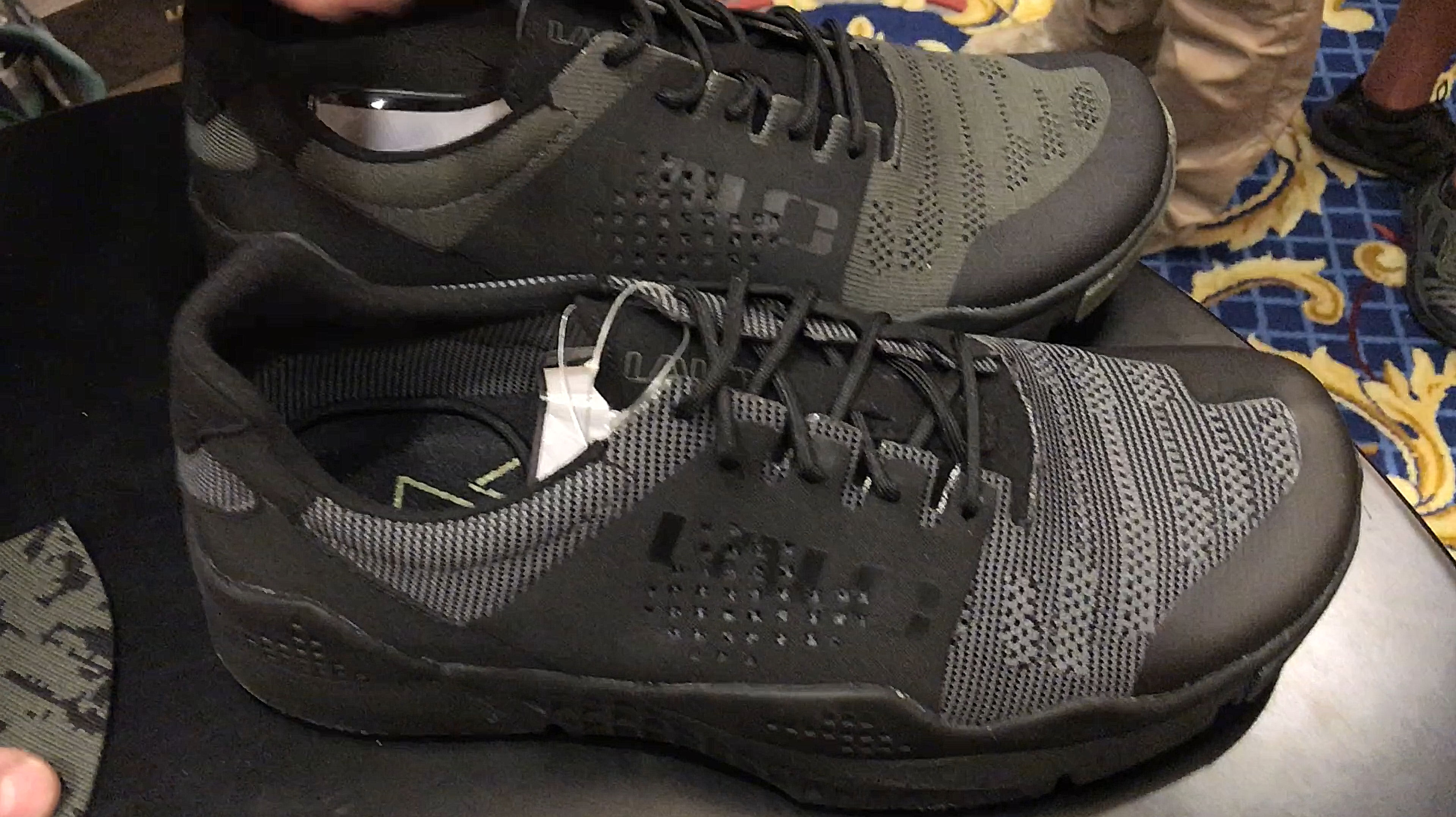
LALO Tactical Prototype Bloodbird and Grinder Sneakers with Digital Combat Camo (Camouflage) Pattern Woven Uppers: A ‘Happy Mistake’! (Video!)

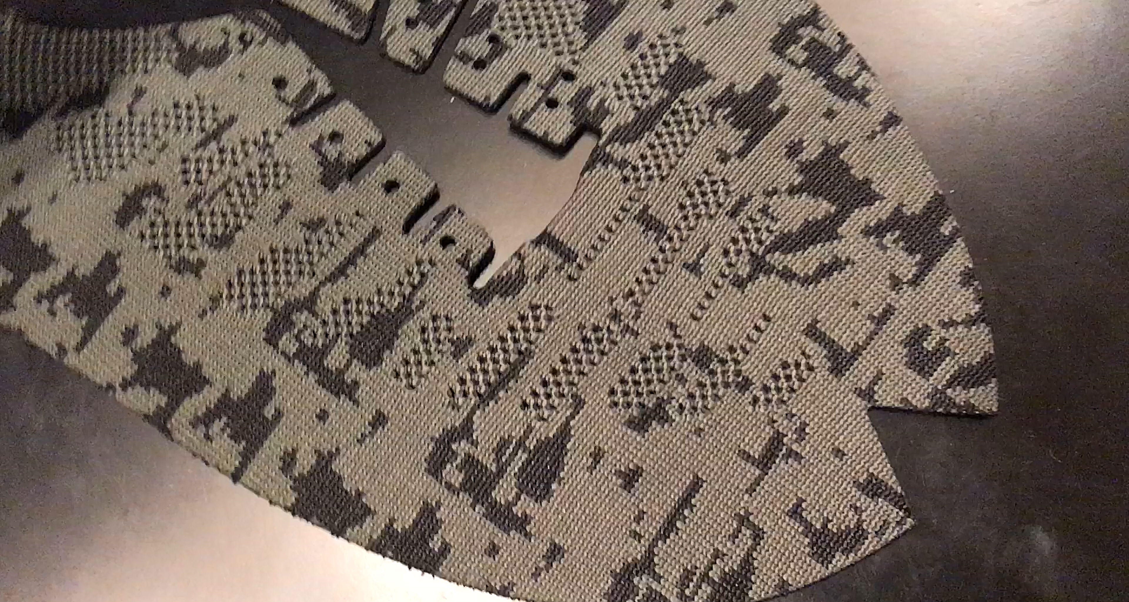
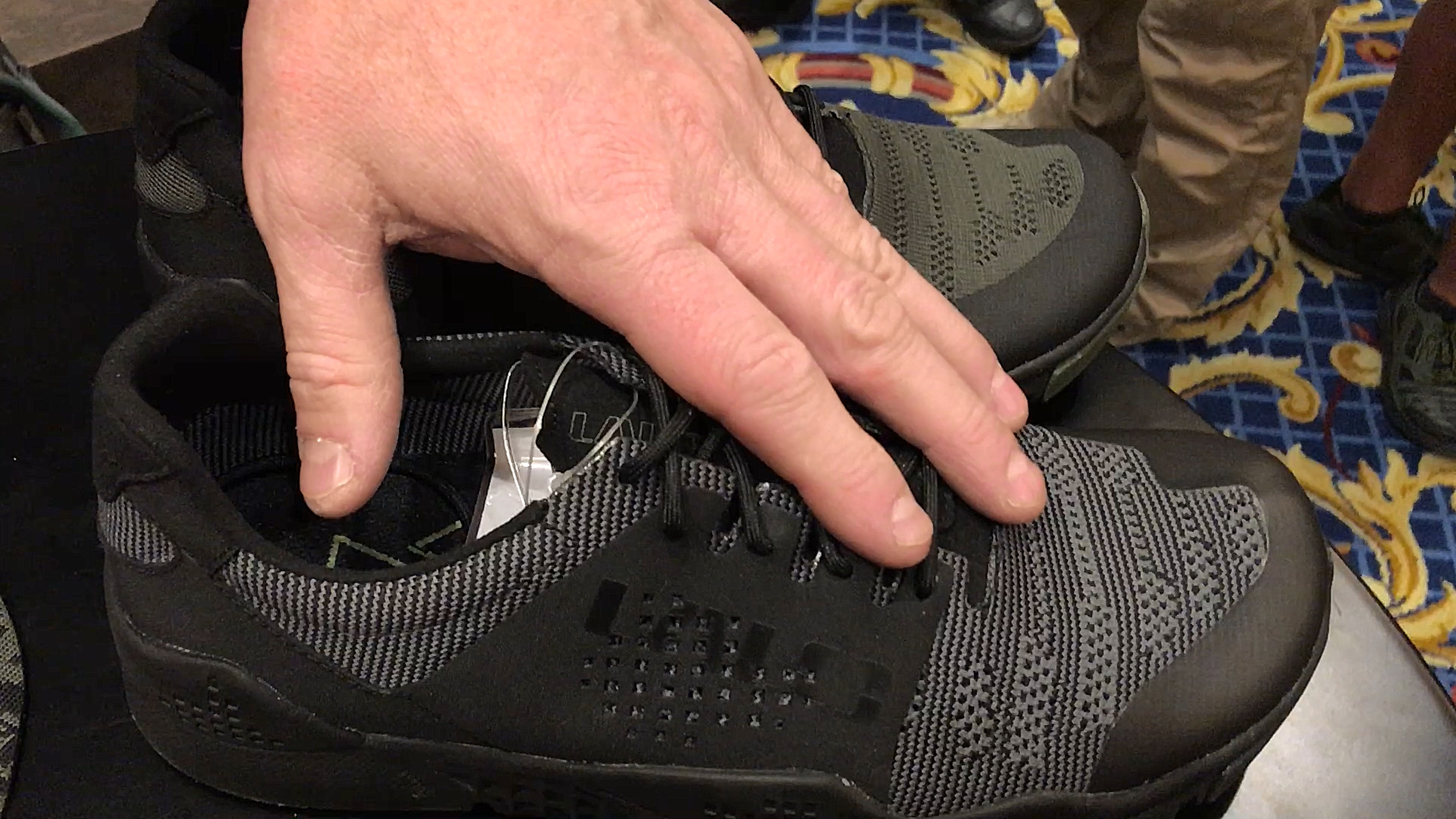
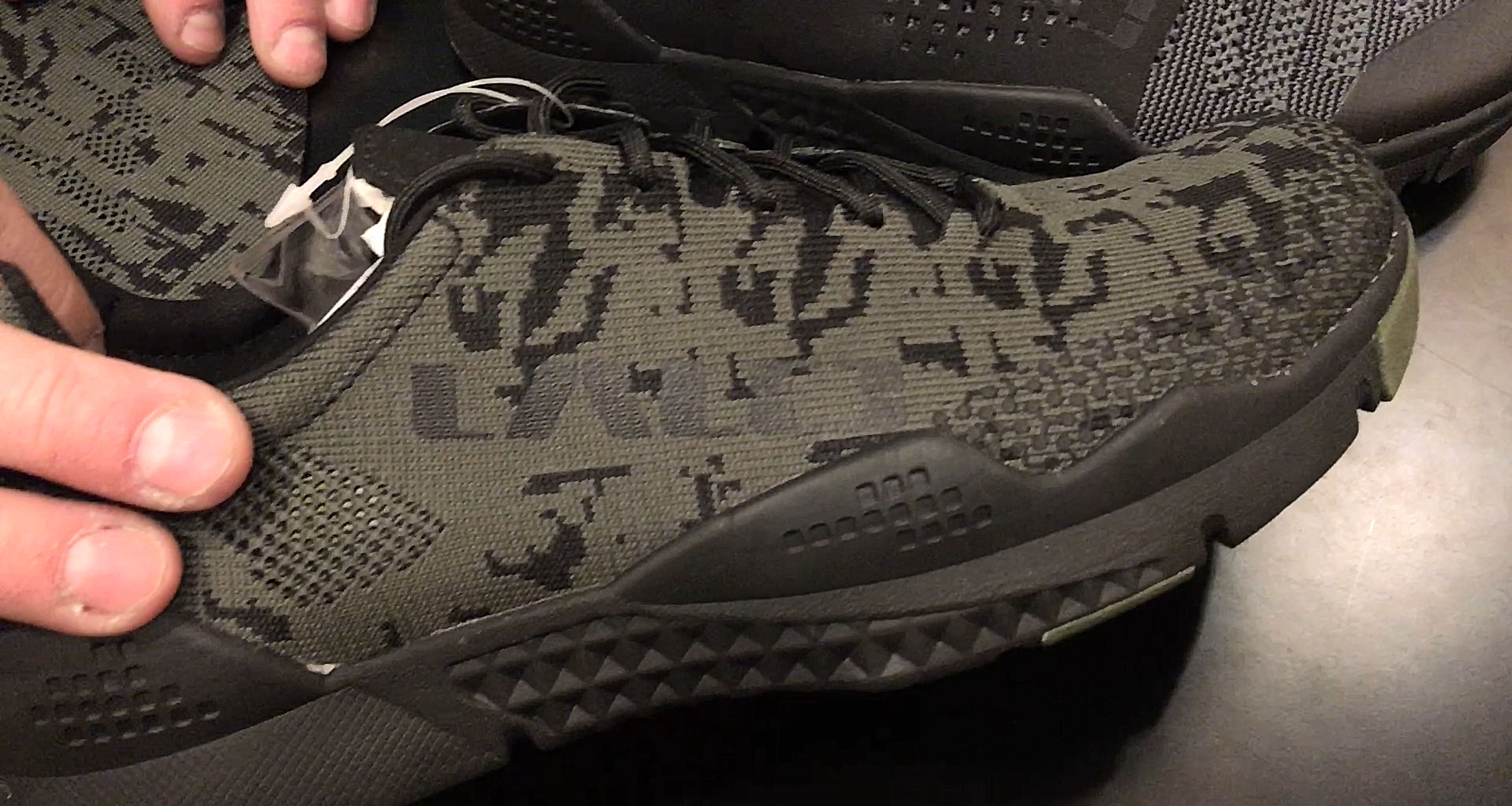
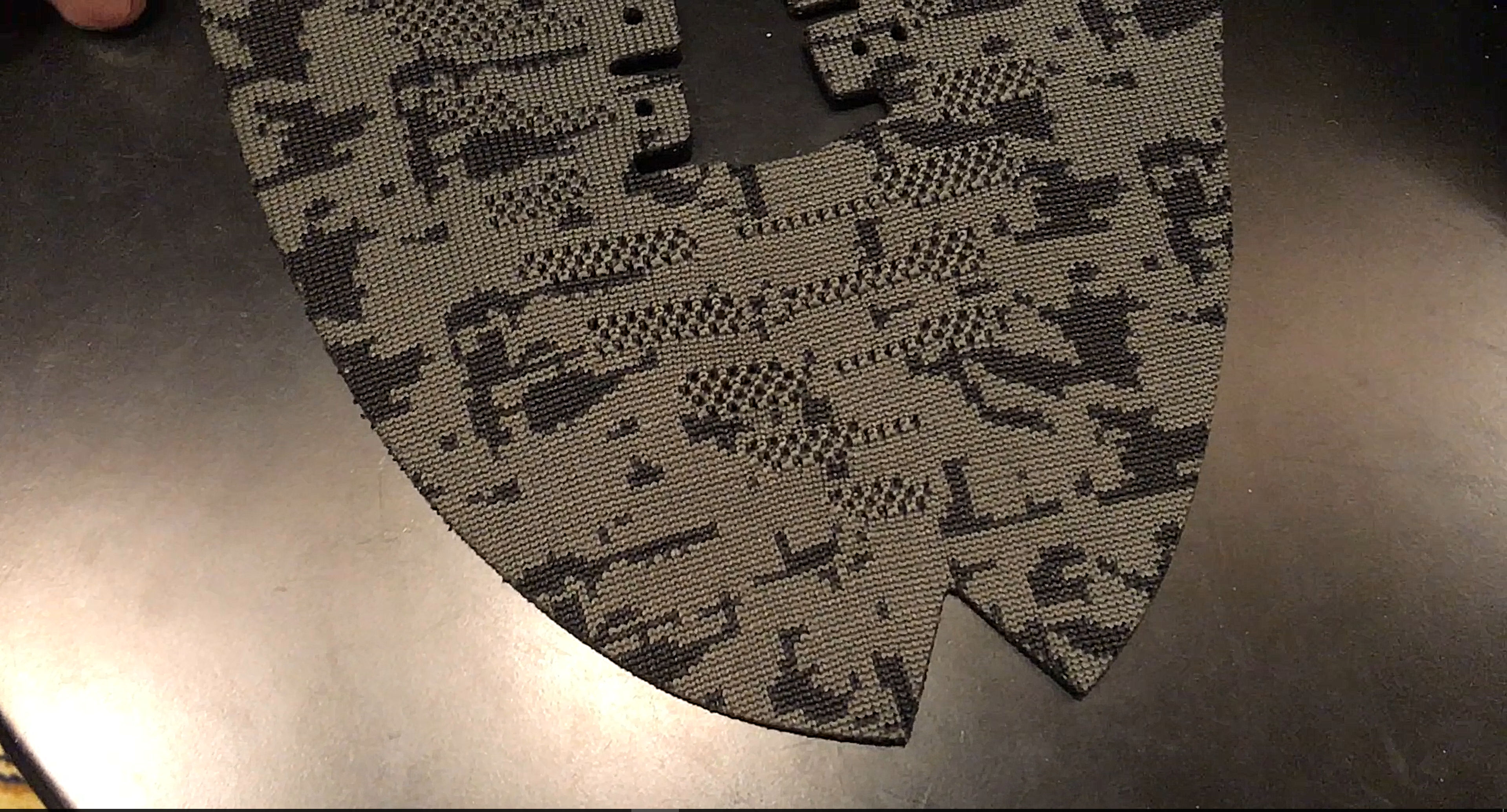
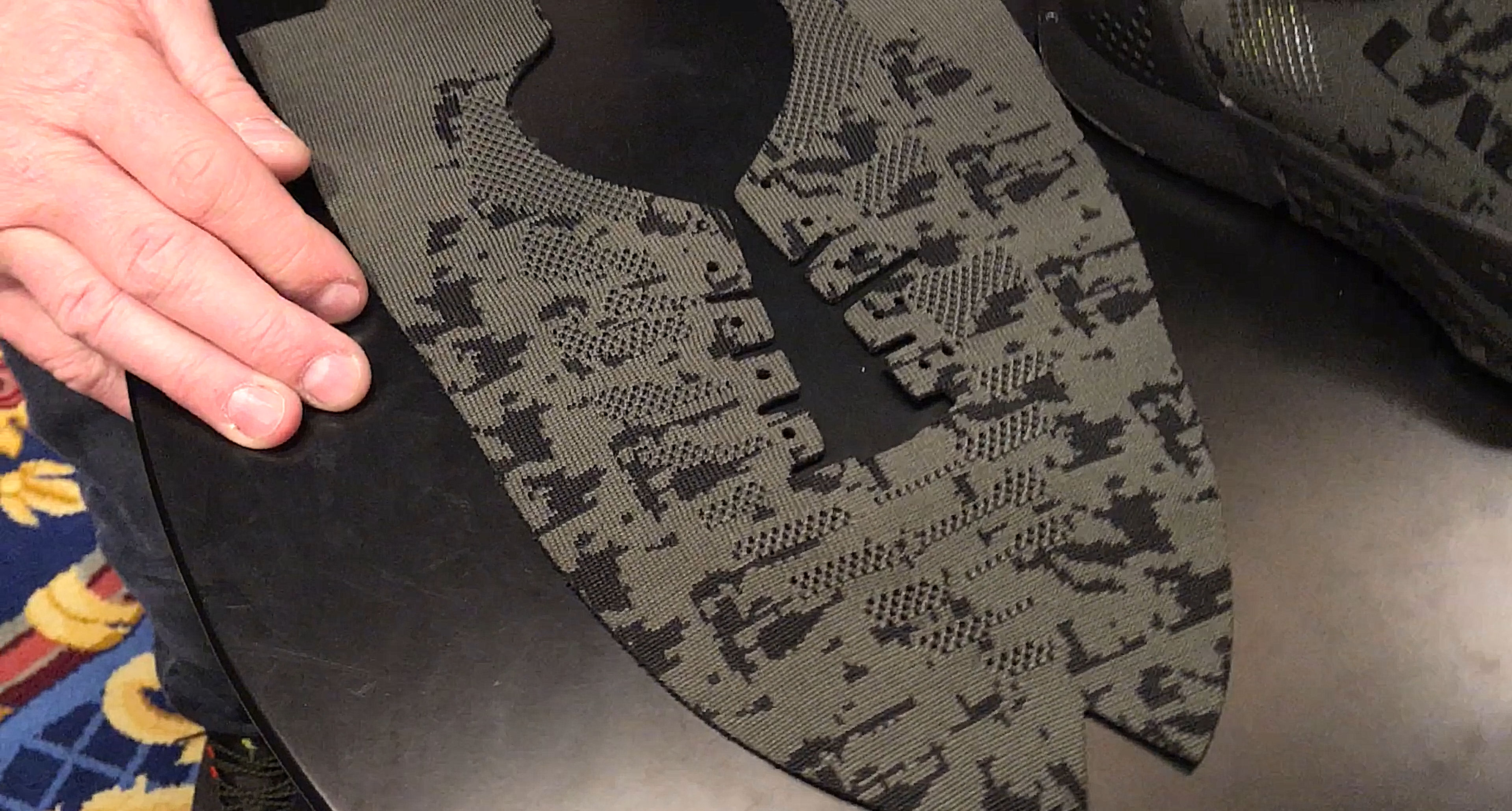
As long as we’re on the subject of LALO Tactical high-tech kicks (sneakers, i.e., running shoes, cross-trainers and weightlifting shoes), we should perhaps also mention the 2019 LALO Tactical Bloodbird and Grinder model prototypes with digital combat camo (camouflage) pattern woven uppers that company founder/president/CEO Jay Taylor showed us, which are the result of a happy accident, or “happy mistake” as DefenseReview (DR) and Mr. Taylor discuss in DR’s video below. Basically, the camo pattern Taylor requested was applied to the woven upper differently than he’d requested it, but he liked the result, so he’s enthusiastically rolling with it.

DR actually enjoys hearing about this kind of scenario, where sometimes the an accidental result is even better than what you were initially trying to achieve. Anyway, the 2019 woven-upper LALO Tactical Grinder and Bloodbird models will be available in the same colorways as the current 2018 models we just wrote about (Jungle and Black, Battleship Grey and Black, Black Ops Black on Black, and Black and Red).

DR digs ’em.

Editor’s Note: Defense Review is going to try to get ahold of some sample LALO Tactical sneakers to actually test them on the road and at the range, as soon as possible. We’d really like to get at least one pair onto DR writer/contributor and chief new-product tester Jeff Gurwitch’s feet. So, keep an eye out for a hands-on review from us.


Company Contact Info:

LALO Tactical
2150 W Washington #208
San Diego, CA 92110
Customer Service Phone: 619-876-5256
International Sales Phone: 619-876-5256 Ext. 105
Customer Service Email: [email protected]
International Sales Email: [email protected]
Website: https://lalo.com

Ingineria suprafeței devine lumină roșie(Surface engineering gets the red light)

Haldele perovskite sunt într-o clasă interesantă de materiale pentru optoelectronică și fotovoltaice. Aceste materiale absoarbe eficient lumina vizibila, au lungimi lungi de difuzie si sunt usor si ieftin de realizat. Performanța dispozitivelor optice poate fi, de asemenea, îmbunătățită prin încorporarea particulelor pe scară nanometrică, care au proprietăți de absorbție și absorbție a luminii mult superioare decât materialul în vrac din care sunt derivate. Deci nu este surprinzător faptul că oamenii de știință sunt dornici să combine aceste două abordări. Provocarea este că particulele mici de perovskite nu sunt întotdeauna stabile din punct de vedere chimic, iar structura lor de cristal atomic este dificil de controlat.

Posted: Apr 25, 2018

Surface engineering gets the red light

(Nanowerk News) A method for chemically stabilizing optical nanocrystals, without degrading their electrical properties, has been developed by scientists at KAUST (Journal of the American Chemical Society, ” Bidentate ligand-passivated CsPbI3 perovskite nanocrystals for stable near-unity photoluminescence quantum yield and efficient red light-emitting diodes”).

Halide perovskites are in an exciting class of materials for optoelectronics and photovoltaics. These materials efficiently absorb visible light, possess long charge-carrier diffusion lengths and are easy and cheap to produce. The performance of optical devices can also be improved by incorporating nanometer-scale particles, which have far superior light-emitting and -absorbing properties than the bulk material from which they are derived. So it is unsurprising that scientists are keen to combine these two approaches. The challenge is that tiny perovskite particles aren’t always chemically stable, and their atomic crystal structure is difficult to control.
Attaching molecules, referred to as ligands, can stabilize a nanocrystal. But this so-called passivation can form an electrically insulating shell around the particle that inhibits their effectiveness in electronic devices.
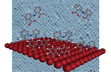
Passivating the surface of perovskite nanocrystals with IDA molecules improves their stability and their optical and electrical properties, making them useful for optoelectronic devices
Passivating the surface of perovskite nanocrystals with IDA molecules improves their stability and their optical and electrical properties, making them useful for optoelectronic devices. (Image: KAUST)
Now, Osman Bakr’s group, and co-workers from KAUST and ShanghaiTech University, has created halide perovskite nanocrystals made from cesium-lead-iodide passivated by 2,2′-iminodibenzoic acid (IDA) ligands. They show that this provides the necessary chemical stability while remaining useful for optoelectronics. And the passivation was simple: just adding IDA powder into the nanocrystal solution and using a centrifuge to remove any excess.
The team chose IDA because it is a bidentate ligand, meaning that it bonds to the nanocrystal at two sites. “The conventional ligands used in these applications, such as oleic acid, are dynamic on the surface of the perovskite nanocrystals and easily come loose,” says Jun Pan, the first author on the paper. “That’s why we apply a double carboxylic group to strongly bind on the surface, which also stabilizes the perovskite crystal phase at room temperature.”
Pan and his team compared the optical properties of both the passivated and unpassivated samples and observed that the treatment improved the photoluminescent quantum yield—a measure of how many photons are emitted for every photon absorbed—from 80 percent to over 95 percent. And while the intensity of light emitted from the unpassivated nanocrystals had dropped significantly five days later, the IDA-treated samples were still emitting light at 90 percent of their initial level 15 days later.
The team demonstrated that their stabilized halide perovskite nanocrystals were suitable for optoelectronic applications by using them to build light-emitting diodes. The red-light generating devices again outperformed the unpassivated control device in terms of maximum luminance and luminous power efficiency.
“The next step is to realize more stable perovskite structures and to create an LED with performance above 10 percent based on perovskite nanocrystals,” says Pan.
Source: King Abdullah University of Science and Technology (KAUST)

Cercetătorii creează componente optice de precizie cu imprimare cu jet de cerneală(Researchers create precision optical components with inkjet printing)

Cercetătorii au dezvoltat o tehnică de tipărire cu jet de cerneală care poate fi utilizată pentru a imprima componente optice, cum ar fi ghidurile de undă. Deoarece abordarea de imprimare poate de asemenea fabrica electronice și microfluidice, ar putea avansa o varietate de dispozitive, cum ar fi senzorii optici utilizați pentru monitorizarea sănătății și dispozitivele de laborator pe cip care integrează și automatizează mai multe funcții de laborator pe un mic circuit sau un cip.

Posted: Apr 25, 2018

Researchers create precision optical components with inkjet printing

(Nanowerk News) Researchers have developed an inkjet printing technique that can be used to print optical components such as waveguides. Because the printing approach can also fabricate electronics and microfluidics, it could advance a variety of devices such as optical sensors used for health monitoring and lab-on-a-chip devices that integrate and automate multiple laboratory functions onto a small circuit, or chip.

„Inkjet printing is a very attractive method for fabricating optical components because the positions and sizes of features can easily be modified and there is virtually no material waste,” said Fabian Lütolf, a member of the research team led by Rolando Ferrini at CSEM in Switzerland. „However, the surface tension of the inks makes it difficult to print lines with a specific height, which is necessary to create a waveguide.”
Inkjet printing is an additive manufacturing technique that uses tiny nozzles like the ones found in desktop inkjet printers to deposit a computer-generated pattern of drops (the „ink”) onto a substrate to build a structure. The researchers discovered that depositing the ink in two steps, rather than the traditional single step, enabled printing of lines with a specific height and with much smoother features than would otherwise be possible. The printed structures are considered to have 2.5 dimensions because although they are not flat, their complexity is limited compared to structures created with traditional 3D printing.
In The Optical Society journal Optics Express („Non-contact printing of optical waveguides using capillary bridges”), the researchers show that their technique can be used to print 2.5D optical waveguides and tapers made of acrylic polymer. The printing concept can also be used with other materials such as metallic inks to make electronics or sucrose mixtures for biodegradable applications.
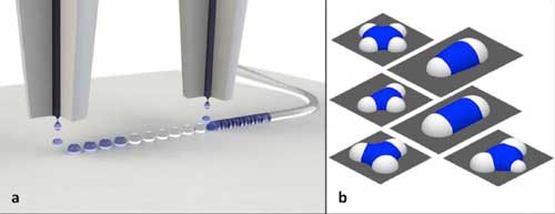
two-step inkjet printing technique that can make waveguides
Researchers developed a two-step inkjet printing technique that can make optical components known as waveguides (a). A series of droplets called pinning caps are first printed (white). Liquid bridges between the pinning caps are then formed by ink deposited in the second print. The pinning caps immobilize the ink and prevent the formation of bulges in the printed line. In addition to making straight lines between two dots, the technique can be used to connect three or more junctions to make corners or sharp edges (b). (Image: Fabian Lütolf, CSEM)
Lütolf points out that although printing of electronics is already used commercially, printing microfluidics is more challenging and prone to the same problems as waveguides. „The fact that our approach could allow components with multiple functionalities to be fabricated with a single printer paves the way toward additive manufacturing of entire integrated circuits on chips,” said Lütolf. „This means that optical components could be added to flexible hybrid electronics and that optoelectronic components such as light sources or detectors could be integrated into printed optical circuits.”

Turning a problem into a solution

Because of surface tension, inks deposited on a substrate tend to bulge or split. Depositing the ink in two steps allowed the researchers to turn the surface tension of the liquid into an advantage. After depositing a series of droplets, the ink printed in the second step seeks to minimize its surface energy by self-aligning between the droplets from the first print. Unlike previous inkjet printing approaches, the researchers did not have to pre-pattern the substrate, which increases the available design space and simplifies fabrication.
To carry out the new technique, a series of droplets called pinning caps are first printed. These spherical caps pin liquid bridges formed by the ink from the second print, forming a configuration that immobilizes the ink and prevents the formation of bulges in the printed line. In addition to making straight lines between two dots, the technique can be used to connect three or more junctions to make corners or sharp edges.
The new technique offers several advantages over classical photolithography, which is typically used to make tiny components on chips. „Inkjet printing doesn’t require a physical mask like photolithography and it is easier to connect components,” said Lütolf. „Also, if you just want to quickly test an idea or vary a parameter, additive manufacturing methods such as inkjet printing only require adaption of the digital design.”
To evaluate the new printing method, the researchers created a polymer waveguide that was 120 microns wide and 31 microns tall with a taper that allowed light from an external laser source to enter the waveguide. They measured the optical loss within the waveguide to be 0.19 dB/cm, only an order of magnitude higher than state of the art waveguides created using photolithography.
„In the paper, we report the first inkjet-printed waveguides with loss characterization,” said Lütolf. „For the applications we envision, the waveguides would carry light for short distances, and not across entire networks. The current level of losses can be tolerated for such applications.”
According to the researchers, the smallest possible waveguides consists of a single droplet of ink, the size of which is limited by the nozzle of the inkjet printer. For the printer used in the study, the narrowest waveguides would be in the 40-micron range with a height of around 10 micrometers. Typical industrial inkjet printers also have similar limits.
„With our current combination of materials and hardware, it’s not possible to make waveguides below 10 micrometers, as typically required for single mode operation. But we are close,” said Lütolf. „There is, however, no fundamental physical limit that would prevent us from printing single mode waveguides.”
He adds that several groups have demonstrated printing capabilities in the submicron range with techniques such as electrohydrodynamic printing (E-jet). It should be possible to combine such instruments with the new inkjet printing technique to create single mode waveguides.
The researchers are now working to optimize the printing method and the ink to further lower the amount of light lost by the waveguide. They are also working to make the inkjet process more applicable for large-scale fabrication and, eventually, commercial implementation.
Source: The Optical Society

Transformarea grafenului în nanosenzori de lumină(Turning graphene into light nanosensors)

Grafenul are multe proprietăți; este, de exemplu, un conductor extrem de bun. Dar nu absorb foarte bine lumina. Pentru a remedia acest aspect limitativ al materialului altfel uimitor, fizicienii recurg la înglobarea unei foi de grafen într-un cristal fotonic plat, care este excelent pentru controlul fluxului de lumină. Combinația oferă grafen cu capacități de absorbție a luminii substanțial îmbunătățite.Acest lucru arată că există un număr de caracteristici care pot fi reglate care pot fi exploatate pentru proiectarea nano-dispozitivelor bazate pe grafen, cum ar fi absorbanții și senzorii sensibili la temperatură.

Posted: Apr 25, 2018

Turning graphene into light nanosensors

(Nanowerk News) Graphene has many properties; it is e.g. an extremely good conductor. But it does not absorb light very well. To remedy this limiting aspect of what is an otherwise amazing material, physicists resort to embedding a sheet of graphene in a flat photonic crystal, which is excellent for controlling the flow of light. The combination endows graphene with substantially enhanced light-absorbing capabilities.

In a new study published in EPJ B („Tunability of temperature-dependent absorption in a graphene-based hybrid nanostructure cavity”), Arezou Rashidi and Abdolrahman Namdar from the University of Tabriz, Iran demonstrate that, by altering the temperature in such a hybrid cavity structure, they can tune its capacity for optical absorption. They explain that it is the thermal expansion and thermo-optical effects which give the graphene these optical characteristics. Potential applications include light sensors, ultra-fast lasers, and systems capable of modulating incoming optical beams.
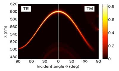
Absorption on the Plane of Incident Angle and Wavelength
Absorption on the plane of incident angle and wavelength. (© Springer)
The authors study the light absorption of the material as a function of temperature, the chemical energy potential, the light polarisation and its incidence angles. To do so, they use a modelling method called the transfer matrix method. They find that for normal light incidence, there is enhanced absorption at room temperature, while the absorption peak is shifted toward the red as the temperature increases.
As light comes in at an angle, the authors show that the absorption peaks are sensitive to the incident angles as well as the polarisation state of the light. They also find that by increasing the incident angle, the peak wavelength is shifted toward the blue.
They conclude that the peak wavelength can be controlled by varying either the temperature or incident angle, as well as the chemical energy potential of graphene. This shows that there are a number of tunable features that could be exploited for the design of graphene-based nano-devices, such as temperature-sensitive absorbers and sensors.
Source: Springer

Un spin de înaltă tehnologie pe mătase de păianjen(A high-tech spin on spider silk)

au dezvoltat un nanofibru polimer puternic, ușor, conductiv termic, izolator electric și biocompatibil.Caracteristicile nanofibrelor sale polimerice îi conferă aplicabilitate în sistemele aerospațiale și auto, inginerie civilă și structurală, dispozitive medicale și robotică.

Posted: Apr 25, 2018

A high-tech spin on spider silk

(Nanowerk News) Spiderman has it figured out.

It’s no coincidence then that when Sheng Shen talks about his work with polymer nanofibers he compares it to a spider spinning its web.
“Just as a spider synthesizes silk from protein polymer to form a fiber with strength similar to high tensile steel, polymers can be spun and drawn to form high-strength materials with exceptionally high thermal conductivity,” said Shen, associate professor of mechanical engineering at Carnegie Mellon University.
Shen and his team have developed a polymer nanofiber that is strong, lightweight, thermally conductive, electrically insulating, and bio-compatible. They accomplished all of this in a single polymer fiber strand measuring less than 100 nanometers (Nature Communications, „Crystalline polymer nanofibers with ultra-high strength and thermal conductivity”).
According to Shen, the potential impact of this development is tremendous. The characteristics of his polymer nanofiber give it application in aerospace and automotive systems, civil and structural engineering, medical devices, and robotics.
Mechanical Engineering faculty member Sheng Shen describes his work developing low-density, multi-functional materials that have a broad range of applications in aerospace, automotive, and biomedical technologies.
In their simplest form, polymers are lots of identical molecules joined together over and over. The molecules could be joined in “simple” chains or more complicated structures. Either way, the resulting polymer has the same characteristics as the molecules used to create it. This means a polymer could be sticky, solid, pliable, or any number of other physical characteristics contained in its molecules.
Traditionally, said Shen, polymers are “the general material platform (used) to develop multifunctional materials,” including plastics, nylons, and rubbers. Polymers are easily processed at relatively low price points, but do have their drawbacks.
Prototypical bulk polymers are often amorphous, meaning their molecule chains are randomly coiled and lacking a defined shape and form. This lack of definition can lead to reduced strength, reduced thermal conductivity, and increased defects like voids and molecule entanglements.
The challenge was to develop a polymer that is both ultra-strong and thermally conductive.
For Shen, the place to do this was at the nano-level. At this level—one-billionth of one meter— Shen can engineer individual molecules to join together in exactly the way he wants them to join together.
“At the nanoscale, the polymer chains become highly oriented and defects that lower strength and thermal conductivity can be eliminated,” Shen said.
The resulting polymer nanofiber has a Young’s Modulus (the measure of the stiffness of a solid material) and a strength that Shen said are 300-times greater than bulk polymers.
As for thermal conductivity, Shen reports that his polymer nanofiber measures a conductivity rate of 100 W/mK. On average, the conductivity rate of steel is 54 W/mK and the rate of iron is 73 W/mK.
“These nanofibers provide a low-cost route to achieving highly effective heat removal in electronic systems,” said Shen. “They can also be bio-compatible heat spreaders for improving patient care.”
To date, Shen and his team have tested single nanofibers. On the strength of the results from those tests, they have turned their attention to creating an innovative manufacturing approach that will allow for the mass production of the polymer nanofibers.
Shen is confident that he and his team have invented a product that will have practical and large-scale impacts sooner rather than later.
“We really believe this is a game-changing technology by transforming polymers from soft and thermally insulating materials to ultra-strong and thermally conductive material,” Shen said.
Source: Carnegie Mellon University

Tehnica nouă realizează o creștere de 32 de ori a efectelor bactericide ale nanosilverului(Novel technique achieves 32-fold increase in bactericidal effects of nanosilver)

au dezvoltat o nouă abordare tehnologică care a generat nanoparticule de argint De 32 de ori capacitatea bactericidă a celor utilizate în prezent în ambalarea produselor alimentare, ortezi, spitale și materiale medicale, printre altele.Aceste nanocompozite au fost compuse din nanoparticule de argint cuplate la un cristal semiconductor de tungsten de argint prin microscopie electronică de transmisie.

Posted: Apr 25, 2018

Novel technique achieves 32-fold increase in bactericidal effects of nanosilver

(Nanowerk News) In recent decades, various research groups in the field of materials science have invested time and resources to answer the following question: is it possible to develop new techniques capable of producing silver particles on a nanometric scale, thus enhancing the optical, catalytic and bactericidal properties of silver? A group of Brazilian investigators has taken a step forward in this contest.

In a research carried out within the Center for Development of Functional Materials (CDMF), one of the Research, Innovation & Dissemination Centers (RIDCs) funded by the São Paulo Research Foundation – FAPESP, they developed a new technological approach that generated silver nanoparticles with 32 times the bactericidal capacity of those currently used in food packaging, orthotics, and hospital and medical materials, among others.
The results of the study, conducted by researchers from the Federal University of São Carlos (UFSCar) and São Paulo State University (UNESP) in Brazil and from Spain’s Jaume I University and the Technical University of Liberec in the Czech Republic, were published in Scientific Reports(„Towards the scale-up of the formation of nanoparticles on α-Ag2WO4 with bactericidal properties by femtosecond laser irradiation”).

New technique provides economic feasibility

A Professor at UFSCar and executive director for the CDMF, Elson Longo says that CDMF’s researchers developed an innovative method of obtaining nanocomposites three years ago. These nanocomposites were comprised of silver nanoparticles coupled to a silver tungstate semiconductor crystal by transmission electron microscopy.
However, the high cost of transmission electron microscopes limited plans of large-scale production of these materials for real-world applications. „The transmission electron microscope used to obtain this material costs approximately 1.3 million euros,” Longo said. The technique involved electron-beam irradiation of silver tungstate, which resulted in promising bactericides whereby the silver tungstate semiconductor attracts bacterial agents that are then are neutralized by silver nanoparticles.
To scale up production of these nanocomposites using a more competitive method, the researchers developed a novel technique consisting of pulsed laser irradiation of a silver tungstate semiconductor, with each pulse lasting only a femtosecond – one millionth of one billionth of a second (10-15 s).
Analysis of the irradiated samples showed that interaction between the silver tungstate semiconductor and the femtosecond laser gave rise to large numbers of microstructures, which they characterized by transmission electron microscopy and found to be of two different types.
„The new technique we developed resulted both in silver nanoparticles left on the semiconductor and in silver clusters,” said the coordinator of the FAPESP-funded research center.
To measure the bactericidal activity of the materials, the researchers placed samples of them in contact with methicillin-resistant strains of Staphylococcus aureus (MRSA), a bacterium that is resistant to numerous antibiotics and is frequently at the root of hospital-acquired infections.
Microscopic analysis showed a 32-fold increase in bactericidal activity for the laser-irradiated samples compared with silver nanoparticles produced by electron-beam irradiation.
„The new technique offers the possibility of obtaining high-performance bactericidal compounds that are easy to produce,” Longo said.

Potential applications

The researchers have applied for a patent on the new technique and the two new classes of silver nanoparticle obtained by the technique.
The idea is to license the technology to Nanox, a spinoff from CDMF based in São Carlos, São Paulo State, and supported by FAPESP’s Innovative Research in Small Business Program (PIPE http://www.bv.fapesp.br/en/3).
„Nanox already sells silver nanoparticles worldwide and could benefit a great deal from the new technique for obtaining the material,” Longo said.
The researchers plan to evaluate use of the material in dental prosthetics and have begun trials to investigate the action of nanocomposites in cancer cells.
Preliminary results of the experiments suggest the nanoparticles can eliminate tumor cells without affecting healthy cells.
Source: Fundação de Amparo à Pesquisa do Estado de São Paulo