
Senzori de detectare utilizati pentru a monitoriza semnele vitale (Near-Field Coherent Sensing Used to Monitor Vital Signs)
au dezvoltat un nou mod de a monitoriza semnele vitale ale pacienților
au dezvoltat un nou mod de a monitoriza semnele vitale ale pacienților
La grosimea monostratului, acest material are proprietățile optice ale unui semiconductor care emite lumină, dar la mai multe straturi proprietățile se schimbă și materialul nu mai emite lumină. Această proprietate este unică pentru acest material”, a spus el. Prin reglarea procesului de creștere a materialului, pelicula subțire rezultată este gravată cu regiuni aleatoare care, în mod alternativ, emit sau nu emite lumină. Când este expus la lumină, acest model se traduce într-o cheie de autentificare unică, care ar putea securiza componentele hardware la un cost minim.
| Posted: Nov 29, 2017 | |
The ultimate defense against hackers may be just a few atoms thick(Nanowerk News) The next generation of electronic hardware security may be at hand as researchers at New York University Tandon School of Engineering introduce a new class of unclonable cybersecurity security primitives made of a low-cost nanomaterial with the highest possible level of structural randomness. Randomness is highly desirable for constructing the security primitives that encrypt and thereby secure computer hardware and data physically, rather than by programming. |
|
| In a paper published in the journal ACS Nano („Physically Unclonable Cryptographic Primitives by Chemical Vapor Deposition of Layered MoS2„), Assistant Professor of Electrical and Computer Engineering Davood Shahrjerdi and his NYU Tandon team offer the first proof of complete spatial randomness in atomically thin molybdenum disulfide (MoS2). The researchers grew the nanomaterial in layers, each roughly one million times thinner than a human hair. By varying the thickness of each layer, Shahrjerdi explained, they tuned the size and type of energy band structure, which in turn affects the properties of the material. | |
 |
|
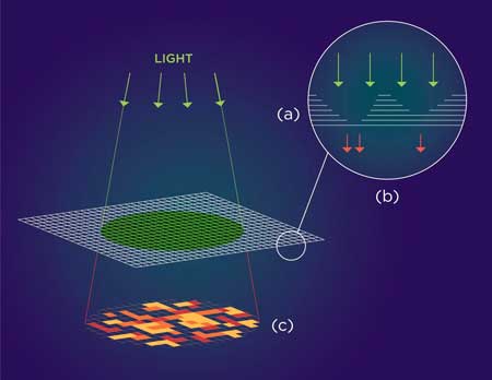
| a) At monolayer thickness, this material has the optical properties of a semiconductor that emits light. At multilayer, the properties change and the material doesn’t emit light. (b) Varying the thickness of each layer results in a thin film speckled with randomly occurring regions that alternately emit or block light. (c) Upon exposure to light, this pattern can be translated into a one-of-a-kind authentication key that could secure hardware components at minimal cost. (Image: Althea Labre, NYU Tandon) | |
| „At monolayer thickness, this material has the optical properties of a semiconductor that emits light, but at multilayer, the properties change, and the material no longer emits light. This property is unique to this material,” he said. By tuning the material growth process, the resulting thin film is speckled with randomly occurring regions that alternately emit or do not emit light. When exposed to light, this pattern translates into a one-of-a-kind authentication key that could secure hardware components at minimal cost. | |
| Shahrjerdi said his team was pondering potential applications for what he described as the beautiful random light patterns of MoS2 when he realized it would be highly valuable as a cryptographic primitive. | |
| This represents the first physically unclonable security primitive created using this nanomaterial. Typically embedded in integrated circuits, physically unclonable security primitives protect or authenticate hardware or digital information. They interact with a stimulus – in this case, light – to produce a unique response that can serve as a cryptographic key or means of authentication. | |
| The research team envisions a future in which similar nanomaterial-based security primitives can be inexpensively produced at scale and applied to a chip or other hardware component, much like a postage stamp to a letter. „No metal contacts are required, and production could take place independently of the chip fabrication process,” Shahrjerdi said. „It’s maximum security with minimal investment.” |
| Source: NYU Tandon School of Engineering |
Constatările ar putea conduce la dezvoltarea unui detector de raze T, deoarece nu a fost încă proiectat un astfel de detector convențional.
Hosono adaugă: „Chiar acum, materialul nostru este bun la detectarea unei radiații terahertz puternice. Provocarea va fi cum să ajustăm sensibilitatea.”
Grupul său a raportat, de asemenea, că anionii de oxigen pot fi înlocuiți cu anioni de aur sau hidrogen în cuști. Folosind aceste anioni diferiți, este posibil să se dezvolte detectoare care emite lumină colorată în viitor
| Posted: Nov 29, 2017 | |
Harnessing the rattling motion of oxygen ions to convert T-rays to visible light(Nanowerk News) Scientists have successfully visualized terahertz radiation, popularly known as T-rays, using a crystal called mayenite (Ca12Al14O33). Their method cleverly utilizes the rattling motion caused by the vibration of oxygen ions inside the cage-like structures of the crystal. |
|
| In recent years, there has been growing interest in developing practical devices based on terahertz technology. With wavelengths longer than infrared light, T-rays are considered safer than conventional imaging systems. They are already used, for example, at airport security checkpoints, and are starting to be used more widely in areas such as medical screening, food inspection and analysis of artworks. The visualization of terahertz light itself, however, has so far proved challenging. | |
| Now, Hideo Hosono of Materials Research Center for Element Strategy, Tokyo Tech and co-workers in Japan, Ukraine and the US have devised a simple approach to convert T-rays to bright, visible light. Their findings have been published in ACS Nano („Rattling of Oxygen Ions in a Sub-Nanometer-Sized Cage Converts Terahertz Radiation to Visible Light”). | |
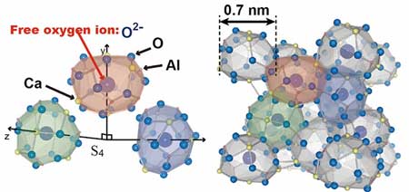
| First, the study involved beaming T-rays onto the mayenite crystal using a gyrotron1. This led to the vibration of oxygen anions2, which collide with the inside walls of the cages within the crystal. Each cage has an inner diameter of 0.4 nanometers and an outer diameter of 0.7 nanometers (see Figure 1). | |
 |
|
| Fig. 1: A schematic representation of the nanoscale cages. The oxygen anions randomly occupy one sixth of the cages. | |
| „The rattling of oxygen ions within the cages promotes upward energy conversion,” Hosono explains. „Strong and frequent collisions of the oxygen ions induce electron transfer to neighboring empty cages. The excitation of the oxygen ions is key to the emission of visible light.” | |
| Spectroscopy measurements confirmed that the visible light originated from vibrations caused by the free-moving oxygen anions. The researchers took care to rule out the possibility of other sources such as black body radiation and surface polarization as reasons behind the production of visible light. | |
| The study is an example of strategic research on functional materials under the Element Strategy initiative supported by Japan’s Ministry of Education, Culture, Sports, Science and Technology (MEXT) and the Japan Science and Technology Agency (JST). | |
| „The crystal in our study is just composed of calcium, aluminium and oxygen, all of which are in the top five of the most abundant elements,” says Hosono. „So, it’s one of the most inexpensive materials, at around 15 cents per kilogram.” | |
 |
|
| Fig. 2: A photograph of the emission of visible light at a terahertz radiation level of 0.21 and output power of 50 W. | |
| Despite its simplicity, Hosono says that the crystal has many exciting properties due to its nanostructure. Drawing on 20 years of research, his group has already succeeded in demonstrating that the material has excellent catalytic properties for ammonia synthesis and superconductivity. | |
| Best known for his pioneering work on iron-based superconductors, Hosono says that the current study marks a new research direction. „Our group has been concentrating on the cultivation of new functionalities using abundant elements, but it’s the first time for me to focus on ionic motion — this is completely new,” he says. | |
| The findings could lead to the development of a T-ray detector, as no such conventional detector has yet been designed. | |
| Hosono adds: „Right now, our material is good at detecting strong terahertz radiation. The challenge will be how to adjust the sensitivity.” | |
| His group has also reported that the oxygen anions can be substituted with gold or hydrogen anions inside the cages. By making use of these different anions, it may be possible to develop detectors that emit different-colored light in future. |
| Source: Tokyo Institute of Technology |
a îmbunătățit considerabil calitatea materialului și performanța filmelor subțiri ale unui material „piezoelectric” fără plumb;Piezoelectricile sunt materiale remarcabile care se deformează la aplicarea unui câmp electric și, invers, produc un curent electric când sunt comprimate. Acestea sunt utilizate în multe aplicații electronice, inclusiv ca servomotoare electromecanice și ca senzori pentru tensiune și accelerație.
| Posted: Nov 29, 2017 | |
Piezoelectrics – Leaving lead behind(Nanowerk News) An advance in fabrication technology has greatly improved the material quality and performance of thin films of a lead-free ‘piezoelectric’ material (Advanced Electronic Materials, „High piezoelectric performance and phase transition in stressed lead-free (1–x)(K,Na)(Sb, Nb)O3-x(Bi,Na,K)ZrO3 thin films”). This development by A*STAR researchers promises to unlock a lead-free alternative to the lead–zircon–titanate (PZT) standard. |
|
 |
|
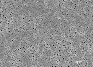
| An electron microscopy image of the KNN thin film showing the controlled formation of the crystalline domains responsible for the piezoelectric effect. (Image: A*STAR Institute of Materials Research and Engineering) | |
| Piezoelectrics are remarkable materials that deform on application of an electric field and, conversely, produce an electric current when compressed. They are used in many electronics applications, including as electromechanical actuators and as sensors for strain and acceleration. Thin films of piezoelectric materials are also being integrated into microelectromechanical systems (MEMS) circuits and devices. | |
| For decades, PZT was the piezoelectric material of choice, since it offered the degree of deformation or sensitivity needed for practical applications. However, PZT contains 60 per cent lead — a toxic metal, which although once commonly used in electronics, has been banned. | |
| An alternative material, which is based on a potassium–sodium–niobate composition and is known as KNN, is being used as a replacement for PZT in many bulk applications. Yet thin films of KNN are problematic because they are subject to a breakdown of composition control and the atomic ordering needed to produce the piezoelectric effect. | |
| Now, Kui Yao and colleagues from the A*STAR Institute of Materials Research and Engineering, in collaboration with National University of Singapore researchers, have shown that a solution-based fabrication method using a painstakingly formulated cocktail of chemical agents can produce thin films of KNN with a piezoelectric performance comparable to PZT. | |
| “It has been challenging to achieve excellent piezoelectric properties in KNN-based thin films because the phase conditions needed for the piezoelectric effect depend very sensitively on composition,” explains Yao. “In KNN, it has been difficult to suppress the loss of volatile elements needed for these conditions.” | |
| Yao and his team overcame this problem by adding a blend of chemical stabilizing agents — refined over more than ten years of research — to the precursor solution used to prepare the KNN thin films. The interactions between the volatile alkali ions in solution and the stabilizing agent suppressed volatilization, allowing the compositions of the resulting films to be well controlled. | |
| “With the film composition under control, we were able to study the phase transitions in the material and their dependence on the chemical composition and stress in the KNN-based thin films,” says Yao. | |
| Through laser measurements combined with theoretical analysis from first-principles simulations, the team confirmed that the performance of their piezoelectric films makes them a viable lead-free alternative to PZT. |
| Source: A*STAR |
Panglici de grafen, care au doar câteva atomi, așa-numitele nanoribbone de grafen, au proprietăți electrice speciale care le fac candidați promițători pentru nanoelectronica viitorului: în timp ce grafenul – un strat subțire de atom de carbon în formă de fagure – este un material conductiv , poate deveni un semiconductor sub formă de nanoribon. Aceasta înseamnă că are un spațiu suficient de mare pentru energie sau bandă, în care nu pot exista stări de electroni: poate fi pornit și oprit – și astfel poate deveni o componentă cheie a nanotranzistorilor.
| Posted: Nov 29, 2017 | |
A transistor made of graphene nanoribbons(Nanowerk News) Transistors based on carbon nanostructures: what sounds like a futuristic dream could be reality in just a few years’ time. An international research team working with Empa has now succeeded in producing nanotransistors from graphene ribbons that are only a few atoms wide, as reported in the current issue of the trade journal Nature Communications („Short-channel field-effect transistors with 9-atom and 13-atom wide graphene nanoribbons”). |
|
| Graphene ribbons that are only a few atoms wide, so-called graphene nanoribbons, have special electrical properties that make them promising candidates for the nanoelectronics of the future: While graphene – a one atom thin, honeycomb-shaped carbon layer – is a conductive material, it can become a semiconductor in the form of nanoribbons. This means that it has a sufficiently large energy or band gap in which no electron states can exist: it can be turned on and off – and thus may become a key component of nanotransistors. | |
| The smallest details in the atomic structure of these graphene bands, however, have massive effects on the size of the energy gap and thus on how well-suited nanoribbons are as components of transistors. On the one hand, the gap depends on the width of the graphene ribbons, while on the other hand it depends on the structure of the edges. Since graphene consists of equilateral carbon hexagons, the border may have a zigzag or a so-called armchair shape, depending on the orientation of the ribbons. While bands with a zigzag edge behave like metals, i.e. they are conductive, they become semiconductors with the armchair edge. | |
| This poses a major challenge for the production of nanoribbons: If the ribbons are cut from a layer of graphene or made by cutting carbon nanotubes, the edges may be irregular and thus the graphene ribbons may not exhibit the desired electrical properties. | |
 |
|
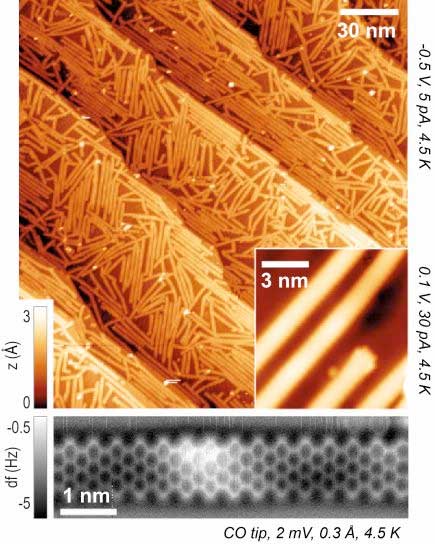
| The microscopic ribbons lie criss-crossed on the gold substrate. (Image: Empa) | |
| Empa researchers in collaboration with the Max Planck Institute for Polymer Research in Mainz and the University of California at Berkeley have now succeeded in growing ribbons exactly nine atoms wide with a regular armchair edge from precursor molecules. The specially prepared molecules are evaporated in an ultra-high vacuum for this purpose. After several process steps, they are combined like puzzle pieces on a gold base to form the desired nanoribbons of about one nanometer in width and up to 50 nanometers in length. | |
| These structures, which can only be seen with a scanning tunneling microscope, now have a relatively large and, above all, precisely defined energy gap. This enabled the researchers to go one step further and integrate the graphene ribbons into nanotransistors. Initially, however, the first attempts were not very successful: Measurements showed that the difference in the current flow between the „ON” state (i.e. with applied voltage) and the „OFF” state (without applied voltage) was far too small. The problem was the dielectric layer of silicon oxide, which connects the semiconducting layers to the electrical switch contact. In order to have the desired properties, it needed to be 50 nanometers thick, which in turn influenced the behavior of the electrons. | |
| However, the researchers subsequently succeeded in massively reducing this layer by using hafnium oxide (HfO2) instead of silicon oxide as the dielectric material. The layer is therefore now only 1.5 nanometers thin and the “on”-current is orders of magnitudes higher. | |
| Another problem was the incorporation of graphene ribbons into the transistor. In the future, the ribbons should no longer be located criss-cross on the transistor substrate, but rather aligned exactly along the transistor channel. This would significantly reduce the currently high level of non-functioning nanotransistors. |
| Source: By Karin Weinmann, Empa |
au descoperit că încorporarea elementului bor în materialul InGaN (indiu-galiu nitrida) aglomerat în LED-uri, făcând materialul mai eficient la producerea luminii ( Aplicată Physics Letters , „aliajele BInGaN aproape de zăbrele, potrivite cu GaN pentru LED-urile vizibile de înaltă eficiență de înaltă eficiență” ).
| Posted: Nov 28, 2017 | |
Atomistic calculations predict that boron incorporation increases the efficiency of LEDs(Nanowerk News) High-power white LEDs face the same problem that Michigan Stadium faces on game day — too many people in too small of a space. Of course, there are no people inside of an LED. But there are many electrons that need to avoid each other and minimize their collisions to keep the LED efficiency high. |
|
| Using predictive atomistic calculations and high-performance supercomputers at the NERSC computing facility, researchers Logan Williams and Emmanouil Kioupakis at the University of Michigan found that incorporating the element boron into the widely used InGaN (indium-gallium nitride) material can keep electrons from becoming too crowded in LEDs, making the material more efficient at producing light (Applied Physics Letters, „BInGaN alloys nearly lattice-matched to GaN for high-power high-efficiency visible LEDs”). | |
 |
|
| Crystal structure of a BInGaN alloy. (Image: Michael Waters and Logan Williams) | |
| Modern LEDs are made of layers of different semiconductor materials grown on top of one another. The simplest LED has three such layers. One layer is made with extra electrons put into the material. Another layer is made with too few electrons, the empty spaces where electrons would be are called holes. Then there is a thin middle layer sandwiched between the other two that determines what wavelength of light is emitted by the LED. | |
| When an electrical current is applied, the electrons and holes move into the middle layer where they can combine together to produce light. But if we squeeze too many electrons in the middle layer to increase the amount of light coming out of the LED, then the electrons may collide with each other rather than combine with holes to produce light. These collisions convert the electron energy to heat in a process called Auger recombination and lower the efficiency of the LED. | |
| A way around this problem is to make more room in the middle layer for electrons (and holes) to move around. A thicker layer spreads out the electrons over a wider space, making it easier for them to avoid each other and reduce the energy lost to their collisions. But making this middle LED layer thicker isn’t as simple as it sounds. | |
| Because LED semiconductor materials are crystals, the atoms that make them up must be arranged in specific regular distances apart from each other. That regular spacing of atoms in crystals is called the lattice parameter. When crystalline materials are grown in layers on top of one another, their lattice parameters must be similar so that the regular arrangements of atoms match where the materials are joined. Otherwise the material gets deformed to match the layer underneath it. Small deformations aren’t a problem, but if the top material is grown too thick and the deformation becomes too strong then atoms become misaligned so much that they reduce the LED efficiency. | |
| The most popular materials for blue and white LEDs today are InGaN surrounded by layers of GaN. Unfortunately, the lattice parameter of InGaN does not match GaN. This makes growing thicker InGaN layers to reduce electron collisions challenging. | |
| Williams and Kioupakis found that by including boron in this middle InGaN layer, its lattice parameter becomes much more similar to GaN, even becoming exactly the same for some concentrations of boron. In addition, even though an entirely new element is included in the material, the wavelength of light emitted by the BInGaN material is very close to that of InGaN and can be tuned to different colors throughout the visible spectrum. This makes BInGaN suitable to be grown in thicker layers, reducing electron collisions and increasing the efficiency of the visible LEDs. | |
| Although this material is promising to produce more efficient LEDs, it is important that it can be realized in the laboratory. Williams and Kioupakis have also shown that BInGaN could be grown on GaN using the existing growth techniques for InGaN, allowing quick testing and use of this material for LEDs. Still, the primary challenge of applying this work will be to fine tune how best to get boron incorporated into InGaN at sufficiently high amounts. But this research provides an exciting avenue for experimentalists to explore making new LEDs that are powerful, efficient, and affordable at the same time. |
| Source: By Andrew McAllister and Emmanouil Kioupakis, University of Michigan |
Bazându-se pe astfel de materiale avansate, cum ar fi perovskitul și nanotuburile de carbon cu un singur perete, noua tehnologie răspunde căldurii prin transformarea de la transparent la colorat. Pe măsură ce fereastra se întunecă, aceasta generează energie electrică. Modificarea culorii este condusă de molecule (metilamină) care sunt absorbite în mod reversibil în dispozitiv.
| Posted: Nov 28, 2017 | |
Researchers develop highly efficient thermochromic windows(Nanowerk News) Thermochromic windows capable of converting sunlight into electricity at a high efficiency have been developed by scientists at the U.S. Department of Energy’s National Renewable Energy Laboratory (NREL). |
|
| Relying on such advanced materials as perovskites and single-walled carbon nanotubes, the new technology responds to heat by transforming from transparent to tinted. As the window darkens, it generates electricity. The color change is driven by molecules (methylamine) that are reversibly absorbed into the device. When solar energy heats up the device, the molecules are driven out, and the device is darkened. When the sun is not shining, the device is cooled back down, and the molecules re-absorb into the window device, which then appears transparent. | |
 |
|
| A scientist at NREL holds a piece of glass that is split between transparent and opaque. Lance Wheeler (front) developed a switchable photovoltaic window along with (from left) Nathan Neale, Robert Tenent, Jeffrey Blackburn, Elisa Miller, and David Moore. (Photo by Dennis Schroeder/NREL) | |
| The NREL-developed demonstration device allows an average of 68 percent of light in the visible portion of the solar spectrum to pass through when it’s in a transparent, or bleached, state. When the window changes color—a process that took about 3 minutes of illumination during testing—only 3 percent is allowed through the window. Existing solar window technologies are static, which means they are designed to harness a fraction of the sunlight without sacrificing too much visible light transmission needed for viewing or the comfort of building occupants. “There is a fundamental tradeoff between a good window and a good solar cell,” said Lance Wheeler, a scientist at NREL. “This technology bypasses that. We have a good solar cell when there’s lots of sunshine and we have a good window when there’s not.” | |
| The proof-of-concept paper published in Nature Communications („Switchable photovoltaic windows enabled by reversible photothermal complex dissociation from methylammonium lead iodide”) established a solar power conversion efficiency of 11.3 percent. “There are thermochromic technologies out there but nothing that actually converts that energy into electricity,” Wheeler said. He is the lead author of the paper, “Switchable Photovoltaic Windows Enabled by Reversible Photothermal Complex Dissociation from Methylammonium Lead Iodide.” | |
| His co-authors, all from NREL, are David Moore, Rachelle Ihly, Noah Stanton, Elisa Miller, Robert Tenent, Jeffrey Blackburn, and Nathan Neale. | |
| In testing under 1-sun illumination, the 1-square-centimeter demonstration device cycled through repeated transparent-tinted cycles, but the performance declined over the course of 20 cycles due to restructuring of the switchable layer. Ongoing research is focused on improving cycle stability. | |
| The path to commercialization of the technology was explored last year during a two-month program called Energy I-Corps. Teams of researchers are paired with industry mentors to learn what customers want of the technology and develop viable ways to reach the marketplace. Lance Wheeler and Robert Tenent, the program lead for window technology at NREL and co-author on the paper, teamed up to develop a market strategy for a product they called SwitchGlaze. The effort was funded by the Emerging Technologies program within the Department of Energy’s Building Technologies Office. | |
| Wheeler said the technology could be integrated into vehicles, buildings, and beyond. The electricity generated by the solar cell window could charge batteries to power smartphones or on-board electronics such as fans, rain sensors, and motors that would open or close the windows as programmed. |
| Source: NREL |
au dezvoltat nanoparticule germaniu cu fotoluminescente imbunatatite, facandu-le potential materiale mai bune pentru celulele solare si sonde de imagistica. Echipa de cercetare a constatat că prin adăugarea de staniu la nucleul de germaniu al nanoparticulei structura sa de zăbrele se potrivește mai bine cu structura zăcământului de acoperire cu sulfură de cadmiu care permite particulelor să absoarbă mai multă lumină
| Posted: Nov 28, 2017 | |
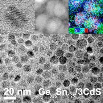
Addition of tin boosts nanoparticle’s photoluminescence(Nanowerk News) Researchers at the U.S. Department of Energy’s Ames Laboratory have developed germanium nanoparticles with improved photoluminescence, making them potentially better materials for solar cells and imaging probes. The research team found that by adding tin to the nanoparticle’s germanium core, its lattice structure better matched the lattice structure of the cadmium-sulfide coating which allows the particles to absorb more light (Chemistry of Materials, „Germanium–Tin/Cadmium Sulfide Core/Shell Nanocrystals with Enhanced Near-Infrared Photoluminescence”). |
|
 |
|
| Electron microscopy images of germanium-tin nanoparticles with a cadmium-sulfide coating. (Image: Ames Laboratory) | |
| “For a photovoltaic material, obviously absorbing light is the first part and converting that solar energy into electrical energy is the second part,” said Ames Laboratory scientist Emily Smith. “So you want a material that does both efficiently. Germanium has some desirable characteristics for photovoltaic materials, but unfortunately it doesn’t absorb light well.” | |
| Part of the problem is that the outside surface of germanium nanoparticles changes over time, primarily from oxidation. Previous work by Ames Laboratory scientist Javier Vela’s group found that coating nanoparticles—commonly referred to as surface passivation—improved the nanoparticles’ ability to absorb light. | |
| “We aren’t actually measuring absorption,” Smith explained, “we measure the luminescence – the amount light given off after a photon is absorbed. ” | |
| “The fact that germanium doesn’t absorb light well is a simple way of saying it’s an indirect bandgap material,” Smith added, “and we are trying to make a more direct bandgap material, one that absorbs light better.” | |
| According to the research literature, the addition of tin appears to improve germanium’s light absorption properties. However, the Ames Laboratory researchers found that even with adding tin, the nanoparticles still required a surface coating. But they also discovered that the relationship between the atomic structure of surface coating and the core material can further enhance the light absorption. | |
| The specific method used is called Successive Ion Layer Adsorption and Reaction or ‘SILAR’, which was first adapted to group IV colloids several years ago. | |
| „We have been developing the expertise required to grow intricate core/shell and other well defined nanoparticles for many years,” Vela said, “Through our collaboration with Emily Smith’s group, we hope to continue making inroads in our ability to manipulate and direct energy flows at the nanoscale.” | |
| Using transmission electron microscopy imaging and powder X-ray diffraction to study the structural characteristics of the nanoparticles and Raman and photoluminescence spectroscopies to quantify lattice strain and photoluminescence behavior, the group found a correlation between the amount of tin in the core and how well the core’s lattice matched that of the cadmium-sulfide outer shell. | |
| “The atoms are in a very specific location within the nanocrystal core and when you apply the shell around the nanocrystal, the atoms of the shell may not match perfectly with the atoms of the core,” Smith said. “With the germanium only material used previously, the core and shell didn’t match perfectly.” | |
| “When we studied the germanium-tin particles, we proposed that they worked better because the spacing of the atoms better matches the spacing of the atoms we used in the coat layer,” she said. “By doing that, you’re getting a more perfect shell that’s less likely to cause chemical changes to the surface of the nanoparticle core.” | |
| Another potential use for this material, besides photovoltaics, is that in microscopy or imaging, researchers often need to “label” a protein or other feature with a nanoparticle “probe” to make it light up so it is easier to see and study. |
| Source: Ames Laboratory |
ferestre termocromice capabile să transforme lumina soarelui în energie electrică cu o eficiență ridicată au fost dezvoltate de oamenii de știință de la USD
Cea mai mare cerere și oportunitate continuă să fie în domeniul armelor transparente, totuși, piața ferestrelor de recunoaștere și a cuptoarelor / ferestrelor senzoriale, realizate de la ALON, continuă să crească și la o rată impresionantă;cantitățile foarte mari de materiale cerute de piața blindată transparentă beneficiază, de asemenea, pe piața senzorilor;Azotul stabilizează structura de cristal spinel cubic pe o gamă largă de compoziție
Compozițiile ceramice transparente policristaline compozite includ granat de ytriu din aluminiu și ytriu, dar spinelurile de aluminiu și aluminat de aluminiu se pare că s-au stabilit ca lideri
stimp25f”]