Graphene nano penseta poate apuca biomolecule individuale(Graphene nano tweezers can grab individual biomolecules)

Graphene, un material fabricat dintr-un singur strat de atomi de carbon, a fost descoperit cu mai mult de un deceniu în urmă și a încântat cercetătorii cu gama sa de proprietăți uimitoare care s-au găsit utilizări în multe aplicații noi, de la microelectronică la celule solare.
Pensetele de grafen, dezvoltate la Universitatea din Minnesota, sunt mult mai eficiente în captarea particulelor în comparație cu alte tehnici folosite în trecut, datorită faptului că grafenul monostrat este un singur atom gros. a realizat penseta de grafen prin crearea unei structuri sandwich în care un material subțire izolant numit dioxid de hafniu este așezat între un metal electrodul pe o parte și grafenul pe cealaltă. Hidroxidul de hafniu este un material utilizat în mod curent în microcipurile avansate de astăzi.

Posted: Dec 01, 2017

Graphene nano tweezers can grab individual biomolecules

(Nanowerk News) Researchers from the University of Minnesota College of Science and Engineering have found yet another remarkable use for the wonder material graphene—tiny electronic “tweezers” that can grab biomolecules floating in water with incredible efficiency. This capability could lead to a revolutionary handheld disease diagnostic system that could be run on a smart phone.

Graphene, a material made of a single layer of carbon atoms, was discovered more than a decade ago and has enthralled researchers with its range of amazing properties that have found uses in many new applications from microelectronics to solar cells.
The graphene tweezers developed at the University of Minnesota are vastly more effective at trapping particles compared to other techniques used in the past due to the fact that monolayer graphene is a single atom thick.
The research study was published in Nature Communications („Graphene-edge dielectrophoretic tweezers for trapping of biomolecules”).
Atomically sharp edges of electrically driven graphene can act as tweezers that rapidly trap biomolecules from the surrounding solution
Atomically sharp edges of electrically driven graphene can act as “tweezers” that rapidly trap biomolecules from the surrounding solution. (Image: In-Ho Lee, University of Minnesota)

The world’s sharpest tweezers

The physical principle of tweezing or trapping nanometer-scale objects, known as dielectrophoresis, has been known for a long time and is typically practiced by using a pair of metal electrodes. From the viewpoint of grabbing molecules, however, metal electrodes are very blunt. They simply lack the “sharpness” to pick up and control nanometer-scale objects.
“Graphene is the thinnest material ever discovered, and it is this property that allows us to make these tweezers so efficient. No other material can come close,” said research team leader Sang-Hyun Oh, a Sanford P. Bordeau Professor in the University of Minnesota’s Department of Electrical and Computer Engineering. “To build efficient electronic tweezers to grab biomolecules, basically we need to create miniaturized lightning rods and concentrate huge amount of electrical flux on the sharp tip. The edges of graphene are the sharpest lightning rods.”
The team also showed that the graphene tweezers could be used for a wide range of physical and biological applications by trapping semiconductor nanocrystals, nanodiamond particles, and even DNA molecules. Normally this type of trapping would require high voltages, restricting it to a laboratory environment, but graphene tweezers can trap small DNA molecules at around 1 Volt, meaning that this could work on portable devices such as mobile phones.
Using the University of Minnesota’s state-of-the-art nanofabrication facilities at the Minnesota Nano Center, electrical and computer engineering Professor Steven Koester’s team made the graphene tweezers by creating a sandwich structure where a thin insulating material call hafnium dioxide is sandwiched between a metal electrode on one side and graphene on the other. Hafnium dioxide is a material that is commonly used in today’s advanced microchips.
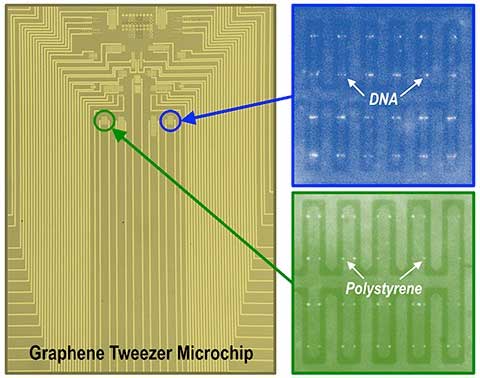
Fluorescence images show DNA molecules and polystyrene nanoparticles trapped on a graphene chip
The University of Minnesota team produced a microchip containing a large array of graphene electronic tweezers. Fluorescence images show DNA molecules and polystyrene nanoparticles trapped on the chip. (Image: Barik et al., University of Minnesota)
“One of the great things about graphene is it is compatible with standard processing tools in the semiconductor industry, which will make it much easier to commercialize these devices in the future,” said Koester, who led the effort to fabricate the graphene devices.
“Since we are the first to demonstrate such low-power trapping of biomolecules using graphene tweezers, more work still needs to be done to determine the theoretical limits for a fully optimized device,” said Avijit Barik, a University of Minnesota electrical and computer engineering graduate student and lead author of the study. “For this initial demonstration, we have used sophisticated laboratory tools such as a fluorescence microscope and electronic instruments. Our ultimate goal is to miniaturize the entire apparatus into a single microchip that is operated by a mobile phone.”

Tweezers that can ‘feel’

Another exciting prospect for this technology that separates graphene tweezers from metal-based devices is that graphene can also “feel” the trapped biomolecules. In other words, the tweezers can be used as biosensors with exquisite sensitivity that can be displayed using simple electronic techniques.
“Graphene is an extremely versatile material,” Koester said. “It makes great transistors and photodetectors, and has the potential for light emission and other novel biosensor devices. By adding the capability to rapidly grab and sense molecules on graphene, we can design an ideal low-power electronics platform for a new type of handheld biosensor.”
Oh agrees that the possibilities are endless.
“Besides graphene, we can utilize a large variety of other two-dimensional materials to build atomically sharp tweezers combined with unusual optical or electronic properties,” said Oh. “It is really exciting to think of atomically sharp tweezers that can be used to trap, sense, and release biomolecules electronically. This could have huge potential for point-of-care diagnostics, which is our ultimate goal for this powerful device.”
Source: University of Minnesota College of Science and Engineering

Un tranzistor realizat din nanofibri de grafen(A transistor made of graphene nanoribbons)

Panglici de grafen, care au doar câteva atomi, așa-numitele nanoribbone de grafen, au proprietăți electrice speciale care le fac candidați promițători pentru nanoelectronica viitorului: în timp ce grafenul – un strat subțire de atom de carbon în formă de fagure – este un material conductiv , poate deveni un semiconductor sub formă de nanoribon. Aceasta înseamnă că are un spațiu suficient de mare pentru energie sau bandă, în care nu pot exista stări de electroni: poate fi pornit și oprit – și astfel poate deveni o componentă cheie a nanotranzistorilor.

Posted: Nov 29, 2017

A transistor made of graphene nanoribbons

(Nanowerk News) Transistors based on carbon nanostructures: what sounds like a futuristic dream could be reality in just a few years’ time. An international research team working with Empa has now succeeded in producing nanotransistors from graphene ribbons that are only a few atoms wide, as reported in the current issue of the trade journal Nature Communications („Short-channel field-effect transistors with 9-atom and 13-atom wide graphene nanoribbons”).

Graphene ribbons that are only a few atoms wide, so-called graphene nanoribbons, have special electrical properties that make them promising candidates for the nanoelectronics of the future: While graphene – a one atom thin, honeycomb-shaped carbon layer – is a conductive material, it can become a semiconductor in the form of nanoribbons. This means that it has a sufficiently large energy or band gap in which no electron states can exist: it can be turned on and off – and thus may become a key component of nanotransistors.
The smallest details in the atomic structure of these graphene bands, however, have massive effects on the size of the energy gap and thus on how well-suited nanoribbons are as components of transistors. On the one hand, the gap depends on the width of the graphene ribbons, while on the other hand it depends on the structure of the edges. Since graphene consists of equilateral carbon hexagons, the border may have a zigzag or a so-called armchair shape, depending on the orientation of the ribbons. While bands with a zigzag edge behave like metals, i.e. they are conductive, they become semiconductors with the armchair edge.
This poses a major challenge for the production of nanoribbons: If the ribbons are cut from a layer of graphene or made by cutting carbon nanotubes, the edges may be irregular and thus the graphene ribbons may not exhibit the desired electrical properties.
Creating a semiconductor with nine atoms
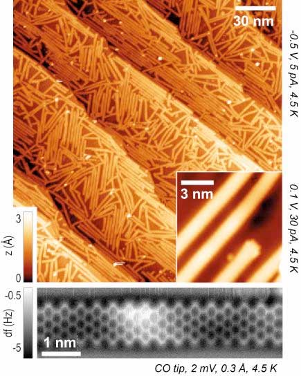
The microscopic ribbons lie criss-crossed on the gold substrate. (Image: Empa)
Empa researchers in collaboration with the Max Planck Institute for Polymer Research in Mainz and the University of California at Berkeley have now succeeded in growing ribbons exactly nine atoms wide with a regular armchair edge from precursor molecules. The specially prepared molecules are evaporated in an ultra-high vacuum for this purpose. After several process steps, they are combined like puzzle pieces on a gold base to form the desired nanoribbons of about one nanometer in width and up to 50 nanometers in length.
These structures, which can only be seen with a scanning tunneling microscope, now have a relatively large and, above all, precisely defined energy gap. This enabled the researchers to go one step further and integrate the graphene ribbons into nanotransistors. Initially, however, the first attempts were not very successful: Measurements showed that the difference in the current flow between the „ON” state (i.e. with applied voltage) and the „OFF” state (without applied voltage) was far too small. The problem was the dielectric layer of silicon oxide, which connects the semiconducting layers to the electrical switch contact. In order to have the desired properties, it needed to be 50 nanometers thick, which in turn influenced the behavior of the electrons.
However, the researchers subsequently succeeded in massively reducing this layer by using hafnium oxide (HfO2) instead of silicon oxide as the dielectric material. The layer is therefore now only 1.5 nanometers thin and the “on”-current is orders of magnitudes higher.
Another problem was the incorporation of graphene ribbons into the transistor. In the future, the ribbons should no longer be located criss-cross on the transistor substrate, but rather aligned exactly along the transistor channel. This would significantly reduce the currently high level of non-functioning nanotransistors.
Source: By Karin Weinmann, Empa

Filtrul de apă de la Grafen se transformă în whisky clar(Graphene water filter turns whisky clear)

Membranele cu oxid de grafen, dezvoltate de Institutul Național de Graphene, au atras atenția pe scară largă asupra aplicațiilor de filtrare a apei și de desalinizare, oferind o soluție potențială pentru deficitul de apă.
Prin utilizarea membranelor ultra-subțiri, acesta este primul experiment clar pentru a arăta cum pot fi filtrați alți solvenți, demonstrând că există potențial pentru nanofiltrarea cu solvenți organici.
Graphene – primul material bidimensional din lume este cunoscut pentru superlativele sale versatilate, poate fi hidrofob și hidrofil, mai puternic decât oțel, flexibil, flexibil și de un milion de ori mai subțire decât părul uman.

Posted: Nov 13, 2017

Graphene water filter turns whisky clear

(Nanowerk News) Previously graphene-oxide membranes were shown to be completely impermeable to all solvents except for water. However, a study published in Nature Materials(„Ultrathin graphene-based membrane with precise molecular sieving and ultrafast solvent permeation”), now shows that we can tailor the molecules that pass through these membranes by simply making them ultrathin.

The research team led by Professor Rahul Nair at the National Graphene Institute and School of Chemical Engineering and Analytical Science at The University of Manchester tailored this membrane to allow all solvents to pass through but without compromising it’s ability to sieve out the smallest of particles.
In the newly developed ultrathin membranes, graphene-oxide sheets are assembled in such a way that pinholes formed during the assembly are interconnected by graphene nanochannels, which produces an atomic-scale sieve allowing the large flow of solvents through the membrane.
This new research allows for expansion in the applications of graphene based membranes from sea water desalination to organic solvent nanofiltration (OSN). Unlike sea water desalination, which separate salts from water, OSN technology separates charged or uncharged organic compounds from an organic solvent.
As an example, Manchester scientists demonstrated that graphene-oxide membranes can be designed to completely remove various organic dyes as small as a nanometre dissolved in methanol.
Prof. Nair said, “Just for a fun, we even filtered whisky and cognac through the graphene-oxide membrane. The membrane allowed the alcohol to pass through but removed the larger molecules, which gives the amber colour. The clear whisky smells similar to the original whisky but we are not allowed to drink it in the lab, however it was a funny Friday night experiment!”
The newly developed membranes not only filter out small molecules but it boosts the filtration efficiency by increasing the solvent flow rate.
Prof. Nair added “Chemical separation is all about energy, various chemical separation processes consume about half of industrial energy useage. Any new efficient separation process will minimize the consumption of energy, which is in high demand now. By 2030, the world is projected to consume 60% more energy than today.”
Dr. Su, who led the experiment added “The developed membranes are not only useful for filtering alcohol, but the precise sieve size and high flux open new opportunity to separate molecules from different organic solvents for chemical and pharmaceutical industries. This development is particularly important because most of the existing polymer-based membranes are unstable in organic solvents whereas the developed graphene-oxide membrane is highly stable.”
Graphene-oxide membranes developed at the National Graphene Institute have attracted widespread attention for water filtration and desalination applications, providing a potential solution to the water scarcity.
By using ultra-thin membranes, this is the first clear-cut experiment to show how other solvents can be filtered out, proving that there is potential for organic solvent nanofiltration.
Graphene- the world’s first two-dimensional material is known for its versatile superlatives, it can be both hydrophobic and hydrophilic, stronger than steel, flexible, bendable and one million times thinner than a human hair.
This research has changed the perception of what graphene-oxide membranes are capable of and how we can use them. By being able to design these membranes to filter specific molecules or solvents, it opens up new potential uses that have previously not been explored.
Source: University of Manchester

TALOS (Tactical Assault Light Operator Suit) – Olimpici de viitori soldati Obtineti usoare abalone Shell bazate pe scalar spumos de metal biomimetic scalar, Carbyne (Linear Acetylenic Carbon) si / sau multistrat Graphene Balistic Armor Composites?(Will TALOS (Tactical Assault Light Operator Suit)-Outfitted Future Soldiers Get Lightweight Abalone Shell-Based Flexible Scalar Biomimetic Metal Foam, Carbyne (Linear Acetylenic Carbon) and/or Multilayer Graphene Ballistic Armor Composites?)

indicând grafenul întins înainte de rupere, care ar trebui să fie promițător, deoarece arată că energia microbulletului este distribuită pe o arie largă a materialului de grafen, în ciuda puncției

48Stim

Suprafața de schimbare îmbunătățește marginile nanofibrelor de grafen

Multe studii au prezis proprietățile nanofibrelor de grafen cu marginile zigzag”, a declarat Guangyu Zhang, autor principal al studiului. „Dar în experimente este foarte greu să faci acest material.”
Anterior, cercetatorii au incercat sa faca nanofibri de grafen prin plasarea foilor de grafen intr-un strat de silice si folosind hidrogenul atomic pentru a etchiza benzi cu marginile zig-zag, un proces cunoscut sub numele de gravura anizotropica. Aceste margini sunt esențiale pentru a modula proprietățile nanoribbonului.
Dar această metodă a funcționat doar bine pentru a face panglici care aveau două sau mai multe straturi de grafen. Neregulile din silicele create de vârfurile și văile electronice scrâșnesc suprafața sa, astfel încât să se creeze margini precise de zigzag pe monostraturile de grafen, a fost o provocar

Posted: Aug 01, 2016

Swapping substrates improves edges of graphene nanoribbons

(Nanowerk News) It is now feasible to make a prized material for spintronic devices and semiconductors – monolayer graphene nanoribbons with zigzag edges.

Miniscule ribbons of graphene are highly sought-after building blocks for semiconductor devices because of their predicted electronic properties. But making these nanostructures has remained a challenge. Now, a team of researchers from China and Japan have devised a new method to make the structures in the lab. Their findings appear in the current issue of Applied Physics Letters („Patterning monolayer graphene with zigzag edges on hexagonal boron nitride by anisotropic etching”).
etched Graphene
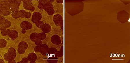
Graphene etched with an underlying silica substrate produces uneven edges (left) but forms precise edges when placed on boron nitride (right). (Image: Guangyu Zhang)
„Many studies have predicted the properties of graphene nanoribbons with zigzag edges,” said Guangyu Zhang, senior author on the study. „But in experiments it’s very hard to actually make this material.”
Previously, researchers have tried to make graphene nanoribbons by placing sheets of graphene over a layer of silica and using atomic hydrogen to etch strips with zigzag edges, a process known as anisotropic etching. These edges are crucial to modulate the nanoribbon’s properties.
But this method only worked well to make ribbons that had two or more graphene layers. Irregularities in silica created by electronic peaks and valleys roughen its surface, so creating precise zigzag edges on graphene monolayers was a challenge. Zhang and his colleagues from the Chinese Academy of Sciences, Beijing Key Laboratory for Nanomaterials and Nanodevices, and the Collaborative Innovation Center of Quantum Matter teamed up with Japanese collaborators from the National Institute for Materials Science to solve the problem.
They replaced the underlying silica with boron nitride, a crystalline material that’s chemically sluggish and has a smooth surface devoid of electronic bumps and pits. By using this substrate and the anisotropic etching technique, the group successfully made graphene nanoribbons that were only one-layer thick, and had well-defined zigzag edges.
„This is the first time we have ever seen that graphene on a boron nitride surface can be fabricated in such a controllable way,” Zhang explained.
The zigzag-edged nanoribbons showed high electron mobility in the range of 2000 cm2/Vs even at widths of less than 10nm – the highest value ever reported for these structures – and created clean, narrow energy band gaps, which makes them promising materials for spintronic and nano-electronic devices.
„When you decrease the width of the nanoribbons, the mobility decreases drastically because of edge defects,” said Zhang. „Using standard lithography fabrication techniques, studies have seen mobility of 100 cm2/Vs or even lower, but our material still exceeds 2000 cm2/Vs even at the sub-10 nanometer scale, demonstrating that these nanoribbons are of very high quality.”
In future studies, extending this method to other kinds of substrates could enable the quick large scale processing of monolayers of graphene to make high-quality nanoribbons with zigzag edges.
Source: American Institute of Physics

Read more: Swapping substrates improves edges of graphene nanoribbons

Borul stimulează sensibilitatea grafenului la gazele nocive

Cercetatorii au descoperit o modalitate de imbunatatire semnificativa a performantei sale prin tratarea foilor de grafenie de inalta calitate cu impuritati de bor. Comparativ cu grafenul original, aceste foi modificate, de exemplu, grafenul dopat de bor, au fost de 27 de ori mai sensibile la detectarea dioxidului de azot și de 105 ori mai sensibile la detectarea amoniacului („Detectarea ultrasensibilă a gazului în grafenul dopat de bor cu suprafață mare”).

Posted: Jul 29, 2016

Boron boosts graphene’s sensitivity to noxious gases

(Nanowerk News) Detecting noxious gases, such as those released from power plants and other sources that can harm the environment, is something graphene does well, but it could be even better.

Researchers discovered a way to significantly improve its performance by peppering high-quality graphene sheets with boron impurities. Compared to pristine graphene, these modified sheets, a.k.a. boron-doped graphene, were 27 times more sensitive at detecting nitrogen dioxide and 105 times more sensitive at detecting ammonia („Ultrasensitive gas detection of large-area boron-doped graphene”).
boron-doped graphene
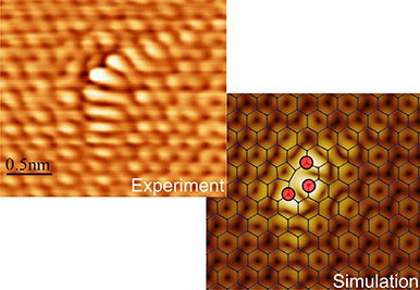
Experimental observations (left) confirm theory-based simulations (right) of boron-doped graphene. Boomerang-shaped atomic features revealed in a centimeter-wide sheet of boron-doped graphene are associated with enhanced sensitivities for nitrogen dioxide and ammonia detection.
Ultrasensitive gas detectors based on this proof-of-principle experiment could monitor environmental health and safety. Sheets of doped graphene with useful electronic and magnetic properties could also find application in field-effect transistors, hydrogen storage, and lithium-ion batteries.
Theory predicts that graphene could be much better at detecting noxious gases if impurities, or dopants, were incorporated into its rigid framework of one-atom-thick carbon. Experimental progress, however, has been limited by a lack of high-quality boron-doped graphene.
Here, scientists grew highly ordered, centimeter-wide sheets of boron-doped graphene and observed, for the first time, boomerang-shaped features corresponding to dopant atoms embedded within graphene’s hexagonal matrix. They characterized the material’s electronic properties, which depend on how impurity atoms incorporate into graphene’s honeycomb lattice and create defects that change the way gases chemically interact with graphene, which in turn alters current flow.
To discover the atomic-level details of how boron doping changes graphene’s properties, the researchers went to the Center for Nanophase Materials Sciences, a DOE Office of Science User Facility at Oak Ridge National Laboratory, for advanced instrumentation and expertise in low-voltage electron microscopy and scanning tunneling microscopy.
Results showed that, compared with pristine graphene, boron doping increases the gas sensing capability of graphene to parts per billion for nitrogen dioxide and parts per million for ammonia.
Source: Department of Energy, Office of Science

Read more: Boron boosts graphene’s sensitivity to noxious gases

Grafine pe bază de electrozi transparenți pentru OLEDS flexibile de înaltă eficiență

Ca o soluție, echipa coreeană de cercetare, care include în continuare profesorii Sung-Yool Choi (Inginerie electrică) și Taek-Soo Kim (Ingineria mecanică) a KAIST și studenții lor, a propus o nouă arhitectură a dispozitivelor care poate maximiza eficiența bazată pe grafen OLED – uri. Ei au fabricat un anod transparent într – o structură compozită în care un TiO 2 straturi , cu un indice ridicat de refracție (high n) și un strat gaură de injecție (HIL) de polimeri conductori , cu un indice de refracție scăzut (low-n) electrozi tip sandwich grafenice . Acesta este un design optic care induce o colaborare sinergică între nivelele înalte n și joase-n pentru a crește reflexia efectivă a TE. Ca rezultat, amplificarea rezonanței cavității optice este maximizată. Rezonanța cavității optice este legată de îmbunătățirea eficienței și a gamei de culori în OLED-urile. În același timp, pierderea de la polaritonul de suprafață a plasmonului (SPP), o cauză majoră pentru emisiile slabe de fotoni în OLED-uri, este de asemenea redusă datorită prezenței polimerilor cu conductivitate joasă.

Read more: Graphene-based transparent electrodes for highly efficient flexible OLEDS

Posted: Jun 03, 2016

Graphene-based transparent electrodes for highly efficient flexible OLEDS

(Nanowerk News) The arrival of a thin and lightweight computer that even rolls up like a piece of paper will not be in the far distant future. Flexible organic light-emitting diodes (OLEDs), built upon a plastic substrate, have received greater attention lately for their use in next-generation displays that can be bent or rolled while still operating.

A Korean research team led by Professor Seunghyup Yoo from the School of Electrical Engineering, KAIST and Professor Tae-Woo Lee from the Department of Materials Science and Engineering, Pohang University of Science and Technology (POSTECH) has developed highly flexible OLEDs with excellent efficiency by using graphene as a transparent electrode (TE) which is placed in between titanium dioxide (TiO2) and conducting polymer layers. The research results were published online on June 2, 2016 in Nature Communications („Synergetic electrode architecture for efficient graphene-based flexible organic light-emitting diodes”).
Application of Graphene-Based OLEDs
This picture shows an OLED with the composite structure of TiO2/graphene/conducting polymer electrode in operation. The OLED exhibits 40.8% of ultrahigh external quantum efficiency (EQE) and 160.3 lm/W of power efficiency. The device prepared on a plastic substrate shown in the right remains intact and operates well even after 1,000 bending cycles at a radius of curvature as small as 2.3 mm. (Image: KAIST) (click on image to enlarge)
OLEDs are stacked in several ultra-thin layers on glass, foil, or plastic substrates, in which multi-layers of organic compounds are sandwiched between two electrodes (cathode and anode). When voltage is applied across the electrodes, electrons from the cathode and holes (positive charges) from the anode draw toward each other and meet in the emissive layer. OLEDs emit light as an electron recombines with a positive hole, releasing energy in the form of a photon. One of the electrodes in OLEDs is usually transparent, and depending on which electrode is transparent, OLEDs can either emit from the top or bottom.
In conventional bottom-emission OLEDs, an anode is transparent in order for the emitted photons to exit the device through its substrate. Indium-tin-oxide (ITO) is commonly used as a transparent anode because of its high transparency, low sheet resistance, and well-established manufacturing process. However, ITO can potentially be expensive, and moreover, is brittle, being susceptible to bending-induced formation of cracks.
Graphene, a two-dimensional thin layer of carbon atoms tightly bonded together in a hexagonal honeycomb lattice, has recently emerged as an alternative to ITO. With outstanding electrical, physical, and chemical properties, its atomic thinness leading to a high degree of flexibility and transparency makes it an ideal candidate for TEs. Nonetheless, the efficiency of graphene-based OLEDs reported to date has been, at best, about the same level of ITO-based OLEDs.
As a solution, the Korean research team, which further includes Professors Sung-Yool Choi (Electrical Engineering) and Taek-Soo Kim (Mechanical Engineering) of KAIST and their students, proposed a new device architecture that can maximize the efficiency of graphene-based OLEDs. They fabricated a transparent anode in a composite structure in which a TiO2 layer with a high refractive index (high-n) and a hole-injection layer (HIL) of conducting polymers with a low refractive index (low-n) sandwich graphene electrodes. This is an optical design that induces a synergistic collaboration between the high-n and low-n layers to increase the effective reflectance of TEs. As a result, the enhancement of the optical cavity resonance is maximized. The optical cavity resonance is related to the improvement of efficiency and color gamut in OLEDs. At the same time, the loss from surface plasmon polariton (SPP), a major cause for weak photon emissions in OLEDs, is also reduced due to the presence of the low-n conducting polymers.
Schematic Device Structure of Graphene-based OLEDs
This picture shows the new architecture to develop highly flexible OLEDs with excellent efficiency by using graphene as a transparent electrode (TE). (Image: KAIST) (click on image to enlarge)
Under this approach, graphene-based OLEDs exhibit 40.8% of ultrahigh external quantum efficiency (EQE) and 160.3 lm/W of power efficiency, which is unprecedented in those using graphene as a TE. Furthermore, these devices remain intact and operate well even after 1,000 bending cycles at a radius of curvature as small as 2.3 mm. This is a remarkable result for OLEDs containing oxide layers such as TiO2 because oxides are typically brittle and prone to bending-induced fractures even at a relatively low strain. The research team discovered that TiO2 has a crack-deflection toughening mechanism that tends to prevent bending-induced cracks from being formed easily.
Professor Yoo said, „What’s unique and advanced about this technology, compared with previous graphene-based OLEDs, is the synergistic collaboration of high- and low-index layers that enables optical management of both resonance effect and SPP loss, leading to significant enhancement in efficiency, all with little compromise in flexibility.” He added, „Our work was the achievement of collaborative research, transcending the boundaries of different fields, through which we have often found meaningful breakthroughs.”
Professor Lee said, „We expect that our technology will pave the way to develop an OLED light source for highly flexible and wearable displays, or flexible sensors that can be attached to the human body for health monitoring, for instance.”
Source: The Korea Advanced Institute of Science and Technology (KAIST)

Read more: Graphene-based transparent electrodes for highly efficient flexible OLEDS

Noua tehnică permite vizualizarea defectelor pe suprafața grafenului

Folosind tehnici imagistice avansate, cercetatorii au descoperit, dass die clusterele de paladiu atașați Selectiv la gemäß suprafața grafen la modele specifice, FUNCȚIE cum reactiv centrele de carbon sunt. Particulele de paladiu individuale rezolva Onto defectelor punctuale, acumulări locale de particule sunt prezente pe defecte mai mari și lanțuri scurte contur defecte liniare

Posted: May 31, 2016

New technique allows to visualize defects on the surface of graphene

(Nanowerk News) The technique, developed by researchers at the Zelinsky Institute of Organic Chemistry in a collaborative project, employs the metal palladium, which interacts with “carbon reactivity centres” found on graphene. Graphene is an incredibly strong one-atom-thick layer of carbon touted to be an excellent conductor of heat and electricity.

Several types of defects on graphene surfaces are known to increase the reactivity of its carbon atoms: i.e. their ability to form chemical bonds. If researchers can locate these defects and manipulate them, they will be able to maximize the use of graphene’s properties.
For example, locating and removing defects is important for applications that require perfectly smooth graphene.
In other applications, such as in catalysis and certain biomedical materials, some defects are actually beneficial because they allow the incorporation of additional elements, such as metals, into the graphene.
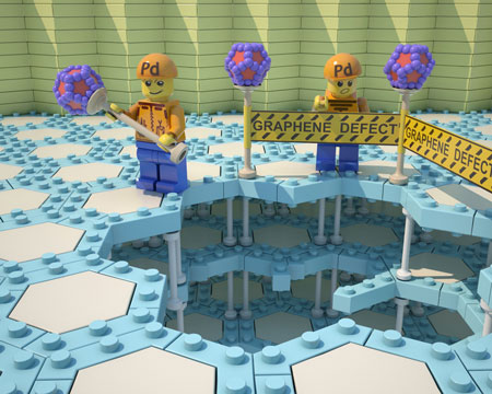
concept of imaging of carbon defect areas by palladium markers
Artistic image on the concept of imaging of carbon defect areas by palladium markers. (Graphene defects marked by Pd). (Image : Ananikov Laboratory, Zelinsky Institute of Organic Chemistry)
When the palladium complex Pd2(dba)3 is dissolved in chloroform, it forms a dark red solution under normal circumstances. But when graphene or another carbon material is added to the solution, the palladium is completely consumed. As a result, the solution turns from dark red to colourless.
Using advanced imaging techniques, the researchers found that the palladium clusters selectively attach to graphene’s surface according to specific patterns, depending on how reactive the carbon centres are. Individual palladium particles settle onto point defects, local accumulations of particles are present on larger defects, and short chains outline linear defects.
These defects are normally invisible under an electron microscope. The palladium particles act like a contrast agent, allowing the spatial imaging of the chemical reactivity, and thus the defects, of graphene layers.
“Metal mapping of carbon materials provides unique insights and reveals hidden information about fascinating properties at the molecular level,” says project leader Professor Valentine Ananikov.
The team’s findings indicate that using palladium markers, more than 2,000 surface defects, or reactivity centres, on graphene can be individually located, per square micrometre of surface area. The researchers say that the unexpected capacity of graphene to accommodate so many reactivity centres challenges scientists to re-examine their understanding of the electronic and structural properties of carbon materials.
Now that the researchers have learned how to recognise and characterise the defects, their next step is to develop a technique to control them. Some defects possess a dynamic nature and have the ability to “migrate” over graphene’s surface. If the researchers can control this migration, they will have a unique opportunity to form materials with customised properties. This is an outstanding direction for future studies, they say
Source: Zelinsky Institute of Organic Chemistry
Subscribe to a free copy of one of our daily
Nanowerk Newsletter Email Digests
with a compilation of all of the day’s news.

Read more: New technique allows to visualize defects on the surface of graphene

Filmul de răcire pe bază de grafen, aproape de producția la scară pilot

metodă eficientă de răcire a electronicii prin utilizarea nanoflacilor grafeni funcționali

Posted: Apr 29, 2016

Cooling graphene-based film close to pilot-scale production

(Nanowerk News) Heat dissipation in electronics and optoelectronics is a severe bottleneck in the further development of systems in these fields. To come to grips with this serious issue, researchers at Chalmers University of Technology have developed an efficient way of cooling electronics by using functionalized graphene nanoflakes. The results will be published in the renowned journal Nature Communications(„Functionalization mediates heat transport in graphene nanoflakes”).

Functionalization Mediates Heat Transport of Graphene Nanoflakes
Functionalization mediates heat transport of graphene nanoflakes. (Image: Johan Liu, credit: Philip Krantz, Krantz Nanoart)
„Essentially, we have found a golden key with which to achieve efficient heat transport in electronics and other power devices by using graphene nanoflake-based film. This can open up potential uses of this kind of film in broad areas, and we are getting closer to pilot-scale production based on this discovery,” says Johan Liu, Professor of Electronics Production at Chalmers University of Technology in Sweden.
The researchers studied the heat transfer enhancement of the film with different functionalized amino-based and azide-based silane molecules, and found that the heat transfer efficiency of the film can be improved by over 76 percent by introducing functionalization molecules, compared to a reference system without the functional layer. This is mainly because the contact resistance was drastically reduced by introducing the functionalization molecules.
Meanwhile, molecular dynamic simulations and ab initio calculations reveal that the functional layer constrains the cross-plane scattering of low-frequency phonons, which in turn enhances in-plane heat-conduction of the bonded film by recovering the long flexural phonon lifetime. The results suggested potential thermal management solutions for electronic devices.
In the research, scientists studied a number of molecules that were immobilized at the interfaces and at the edge of graphene nanoflake-based sheets forming covalent bonds. They also probed interface thermal resistance by using a photo-thermal reflectance measurement technique to demonstrate an improved thermal coupling due to functionalization.
„This is the first time that such systematic research has been done. The present work is much more extensive than previously published results from several involved partners, and it covers more functionalization molecules and also more extensive direct evidence of the thermal contact resistance measurement,” says Johan Liu.
Source: Chalmers University of Technology

Read more: Cooling graphene-based film close to pilot-scale production

Servirea nanopachetelor MoO3 proaspete, curate și monostrat subțiri ( Serving up fresh, clean, and monolayer-thin MoO3 nanosheets )

Molibden (α-MoO 3 ) conține , de asemenea , astfel de straturi 2D, care sunt legate între ele prin slabe forțe van der Waals care cauzeaza o molecula care urmeaza sa fie atras sau impins departe de o altă moleculă.
Structura unică stratată face ca α-MoO 3 să fie un material atrăgător pentru utilizarea în bateriile litiu-ion și dispozitivele electrochromice, cum ar fi ferestrele „inteligente” care controlează absorbția luminii solare în clădiri și oglinzile retrovizoare auto-dim care protejează șoferii de lumini de mare viteză .

Posted: Apr 09, 2016

Serving up fresh, clean, and monolayer-thin MoO3 nanosheets

(Nanowerk News) The 2010 Nobel Prize in physics was awarded to Manchester scientists Andre Geim and Konstantin Novoselov for their pioneering work with graphene, a 1-atom-thick, two-dimensional (2D) network of carbon that may revolutionize computing and electronics. Molybdenum trioxide (α-MoO3) also contains such 2D layers, which are linked together through weak van der Waals forces that cause a molecule to become attracted or pushed away from another molecule.

The unique layered-structure makes α-MoO3 an attractive material for use in lithium ion batteries and electrochromic devices, such as „smart” windows that control solar light absorption in buildings and auto-dim rearview mirrors that protect drivers from high-beam lights.
Schematic representation of the re-evaporation of ?-MoO<span class='subscript' style=3 molecular fragments from the surface of a single monolayer during film growth” border=”0″ align=”middle”>
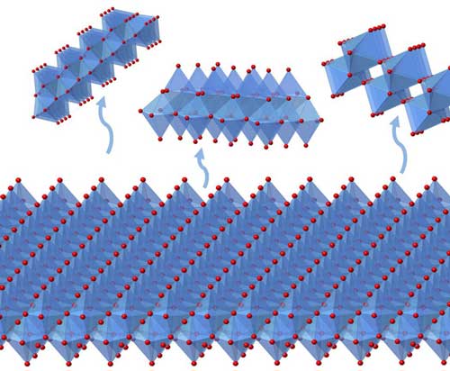
Schematic representation of the re-evaporation of α-MoO3 molecular fragments from the surface of a single monolayer during film growth. At the optimum substrate temperature, only one monolayer “sticks” to the substrate because of strong interaction between the two; all other monolayers desorb because of weak van der Waals interaction with the first layer.
Results
Materials scientists at Pacific Northwest National Laboratory have overcome a set of challenges in synthesis and isolation of ultra-thin α-MoO3 layers. They developed a reproducible method for growing α-MoO3 sheets down to a monolayer in thickness. They used a thin-film deposition technique, molecular beam epitaxy (MBE), to synthesize α-MoO3. A stable oxide substrate provided the needed template (Nanoscale, „Iso-oriented Monolayer α-MoO3(010) Films Epitaxially Grown on SrTiO3(001)”).
The secret to growing monolayer-thin α-MoO3 is multi-faceted. The scientists’ success hinged on the right substrate that provides lateral confinement to the α-MoO3, and the carefully identified growth temperature, which allows α-MoO3 seeds to evolve, grow, but stop right at the monolayer thickness. Their results, which can greatly advance our current understanding on the material’s physical and chemical properties, appear in the scientific journal Nanoscale.
Why It Matters
Besides electrochemical and catalytic applications, ultra-thin α-MoO3 has also demonstrated its potential use in thin-film pseudocapacitors, light-emitting diodes, plasmon resonance generators, and biosensors. It is critical to be able to synthesis and isolate such 2D materials in a contamination-free environment (ultra-high vacuum) to better understand their intrinsic properties. The PNNL science team was able to meet these high standards by combining instrumentation and capabilities in the Environmental Molecular Sciences Laboratory (EMSL), a DOE national user facility.
Methods
„To grow the layers, we evaporate high-purity MoO3 powders held in a ceramic cup in ultra-high vacuum and put a substrate in front to collect the molecules,” said Dr. Yingge Du, lead scientist on the project. The evaporated MoO3 molecules will condense and form a well-ordered thin film on the heated substrate.
Du likens the substrate to a Lego© base plate. „If you throw atoms together randomly, they will stick together like a pile of Lego pieces in a random, messy way. But with a good base template, you can position the Legos in an ordered fashion, and make nice structures.”
And, MoO3 film growth is temperature sensitive. „At lower substrate temperatures, the material will grow as amorphous layers and become thicker and thicker. At higher temperatures, unwanted phases and structures start to evolve,” Du said. „We were extremely delighted that a very narrow temperature window was found for us to grow this material as a single monolayer.”
The correct temperature-in this case, 450°C-allows a crystalline layer to form on the substrate, stabilized by interfacial chemistry. However, the growth of subsequent MoO3 layers is suppressed by material re-evaporation from the substrate. The high substrate temperature and weak van der Waals bonding between adjacent MoO3 layers allow a self-limiting growth process, which provides a highly reliable technique for MoO3 to form and stay as a monolayer.
„Using traditional methods, these nanomaterials are hard to grow or isolate. The trick is to find the optimal temperature that not only provides enough thermal energy to start the crystal structure, but also is high enough to de-adsorb additional layers,” said Du.
What’s Next?
The research also paves the way to creating phase-pure, thicker films by lowering the growth temperature once the monolayer template is formed. The team plans to further investigate the electronic, transport, and catalytic properties of these films using various in situ spectroscopy and microscopy techniques at EMSL.
Source: Pacific Northwest National Laboratory

Read more: Serving up fresh, clean, and monolayer-thin MoO3 nanosheets

Grafenul alunecă ușor peste aur

În viitor, grafenul ar putea fi folosit ca strat de acoperire extrem de subțire, rezultând o pierdere de energie aproape între zero între piesele mecanice. Aceasta se bazează pe lubrifiția excepțional de mare – sau așa-numita super-lubricitate – a carbonului modificat sub formă de grafen. Aplicarea acestei proprietăți la dispozitivele mecanice și electromecanice nu numai că ar îmbunătăți eficiența energetică, ci și va prelungi considerabil durata de viață a echipamentului.

Posted: Mar 04, 2016

Graphene slides smoothly across gold

(Nanowerk News) Since it produces almost no friction at all, graphene could drastically reduce energy loss in machines when used as a coating, as researchers report in the journal Science („Superlubricity of graphene nanoribbons on gold surfaces”).

Graphene Slides Smoothly Across Gold
A graphene nanoribbon was anchored at the tip of an atomic force microscope and dragged over a gold surface. The observed friction force was extremely low. (Image: University of Basel, Department of Physics)
In future, graphene could be used as an extremely thin coating, resulting in almost zero energy loss between mechanical parts. This is based on the exceptionally high lubricity–or so-called superlubricity–of modified carbon in the form of graphene. Applying this property to mechanical and electromechanical devices would not only improve energy efficiency but also considerably extend the service life of the equipment.
Fathoming out the causes of the lubricant behavior
An international community of physicists have studied the above-average lubricity of graphene using a two-pronged approach combining experimentation and computation. To do this, they anchored two-dimensional strips of carbon atoms–so-called graphene nanoribbons–to a sharp tip and dragged them across a gold surface. Computer-based calculations were used to investigate the interactions between the surfaces as they moved across one another. Using this approach, the research team is hoping to fathom out the causes of superlubricity; until now, little research has been carried out in this area.
By studying the graphene nanoribbons, the researchers hope to learn about more than just the slip behavior. Measuring the mechanical properties of the carbon-based material also makes sense because it offers excellent potential for a whole range of applications in the field of coatings and micromechanical switches. In future, even electronic switches could be replaced by nanomechanical switches, which would use less energy for switching on and off than conventional transistors.
The experiments revealed almost perfect, frictionless movement. It is possible to move graphene nanoribbons with a length of 5 to 50 nanometers using extremely small forces (2 to 200 piconewtons). There is a high degree of consistency between the experimental observations and the computer simulation.
A discrepancy between the model and reality appears only at greater distances (five nanometers or more) between the measuring tip and the gold surface. This is probably because the edges of the graphene nanoribbons are saturated with hydrogen, which was not accounted for in the simulations.
„Our results help us to better understand the manipulation of chemicals at the nano level and pave the way for creating frictionless coatings,” write the researchers.
Source: Technische Universität Dresden

Read more: Graphene slides smoothly across gold