
Aramid Flame Retardant Fabric (Tesatura retardanta cu flacara Aramid)
rezistent la aramid
rezistent la aramid
Cercetătorii de la Centrul de Cercetare Științifică avansată (ASRC) de la Centrul Universitar din New York și de la City College din New York (CCNY) au dezvoltat un metamaterial care poate transporta sunetul în moduri neobișnuit de robuste de-a lungul margini și localizați-o în colțurile sale.
Conform unui nou articol publicat în Nature Materials ( „Observarea stărilor acustice topologice ordonate protejate de simetria chirală generalizată” ), materialul nou conceput creează o structură acustică robustă care poate controla în moduri neobișnuite propagarea și localizarea sunetului chiar și atunci când imperfecțiunile de fabricare există. Această proprietate unică poate îmbunătăți tehnologiile care utilizează unde sonore, cum ar fi sonare și dispozitive cu ultrasunete, făcându-le mai rezistente la defecte.In mod fundamental, vom arata ca este posibil sa se permita noi forme de transport sunet mult mai robuste decat cele obisnuite. Aceste descoperiri pot gasi aplicatii in imagistica cu ultrasunete, acustica subacvatica si tehnologia sonar
| Jan 01, 2019 | |
Researchers discover a metamaterial with inherently robust sound transport(Nanowerk News) Researchers at the Advanced Science Research Center (ASRC) at The Graduate Center of The City University of New York and at the City College of New York (CCNY) have developed a metamaterial that can transport sound in unusually robust ways along its edges and localize it at its corners. |
|
| According to a new paper published in Nature Materials („Observation of higher-order topological acoustic states protected by generalized chiral symmetry”), the newly engineered material creates a robust acoustic structure that can control in unusual ways the propagation and localization of sound even when fabrication imperfections exist. This unique property may improve technologies that use sound waves, such as sonars and ultrasound devices, making them more resistant to defects. | |
| The research is a collaboration between the labs of Alexander Khanikaev, a professor in the electrical engineering and physics departments at CCNY who is also affiliated with the ASRC, and of Andrea Alù, director of the ASRC’s Photonics Initiative. Their advance is based on work that brought a field of mathematics called topology into the materials science world. Topology studies properties of an object that are not affected by continuous deformations. For instance, a donut is topologically equivalent to a plastic straw, as they both have one hole. One could be molded into the other by stretching and deforming the object, and without tearing it or adding new holes. | |
| Using topological principles, researchers predicted and later discovered topological insulators–special materials that conduct electric currents only on their edges, not in the bulk. Their unusual conduction properties stem from the topology of their electronic band gap, and they are therefore unusually resistant to continuous changes, such as disorder, noise or imperfections. | |
| „There has been a lot of interest in trying to extend these ideas from electric currents to other types of signal transport, in particular to the fields of topological photonics and topological acoustics,” Alù says. „What we are doing is building special acoustic materials that can guide and localize sound in very unusual ways.” | |
| To design their novel acoustic metamaterial, the team 3D-printed a series of small trimers, arranged and connected in a triangular lattice. Each trimer unit consisted of three acoustic resonators. The rotational symmetry of the trimers, and the generalized chiral symmetry of the lattice, gave the structure unique acoustic properties that stem from the topology of their acoustic bandgap. | |
| The acoustic modes of the resonators hybridized, giving rise to an acoustic band structure for the whole object. As a result, when sound is played at frequencies outside the band gap it can propagate through the bulk of the material. But when sound is played at frequencies inside the band gap, it can only travel along the triangle’s edges or be localized at its corners. This property, Alù says, is not affected by disorder or fabrication errors. | |
| „You could completely remove a corner, and whatever is left will form the lattice’s new corner, and it will still work in a similar way, because of the robustness of these properties,” Alù said | |
| To break these properties, researchers had to reduce the symmetry of the material by, for example, changing the coupling between resonator units, which changes the topology of the band structure and thus changes the material’s properties. | |
| „We have been the first to build a topological metamaterial for sound supporting different forms of topological localization, along its edges and at its corners.”, Khanikaev said. „We also demonstrated that advanced fabrication techniques based on 3D printed acoustic elements can realize geometries of arbitrary complexity in a simple and flexible platform, opening disruptive opportunities in the field of acoustic materials. We have been recently working on even more complex 3D metamaterial designs based on these techniques, which will further expand the properties of acoustic materials and expand capabilities of acoustic devices”. | |
| „We’re showing, fundamentally, that it is possible to enable new forms of sound transport that are much more robust than what we are used to. These findings may find applications in ultrasound imaging, underwater acoustics and sonar technology,” Alù said. |
| Source: Advanced Science Research Center, GC/CUNY |
Un material proiectat de inginerii chimici ai MIT poate reacționa cu dioxidul de carbon din aer, să crească, să se consolideze și chiar să se repare
Programul de chimie Al își propune să accelereze crearea de noi molecule de înaltă performanță pentru nevoile de apărare
au reusit sa creeze materiale asemanatoare cu grafenul dintr-o sinteza moleculara. Acestea sunt materiale MUV-1, robuste, cu o mare versatilitate chimică, care sunt capabile să aibă proprietăți fizice diferite, cum ar fi magnetismul.Această prelucrabilitate, adăugată faptului că MUV-1 are stabilitate mecanică și chimică, a permis oamenilor de știință să construiască membrane bazate pe aceste materiale și să izoleze primele monostraturi magnetice pe baza chimiei de coordonare.
| Posted: Sep 20, 2018 | |
Scientists develop 2D materials capable of having magnetism(Nanowerk News) An international team of physicists and chemists, headed by Eugenio Coronado and Guillermo Mínguez Espallargas, researchers of Valencia University’s Molecular Science Institute (ICMol) have been able to create materials similar to graphene from a molecular synthesis. These are MUV-1, robust materials with great chemical versatility that are capable of having different physical properties such as magnetism. |
|
| Results of the research have been published in Nature Chemistry („Isoreticular two-dimensional magnetic coordination polymers prepared through pre-synthetic ligand functionalization”). | |
| Different bidimensional metallic-organic materials have been designed in this project – the MUV-1, or Materials of the University of Valencia – from a molecular synthesis. Unlike with graphene and other bidimensional materials, this new synthesis makes it possible to modify the surface’s properties at will, changing it for example from hydrophobic to hydrophilic, or adding physical properties such as magnetism, which are complicated to insert. | |
| The study opens the possibility to integrate and apply these materials in different technological areas such as nanoelectronics and spintronics, or to the development of ultrasensitive molecular sensors, which can recognise and selectively detect certain molecules. | |
| Since the discovery of graphene – the first bidimensional material comprised of a layer of carbon atoms -, numerous inorganic bidimensional materials have been created. One of the problems of said materials is that it is not possible to modify their properties by anchoring the molecules of its surface, which blocks the addition of new properties or the improvement of its processability. | |
| Furthermore, the study of magnetism in bidimensional materials of an inorganic nature known to date represents a scientific challenge, as they are all chemically unstable in environmental conditions. | |
| The new molecular synthesis of bidimensional materials that the ICMol proposes to the international scientific community offers solutions to both problems. On one hand, the possibility to functionalise these 2D materials at will makes it possible to easily alter their properties, making them hydrophobic or hydrophilic, for example. | |
| Said processability, added to the fact that the MUV-1 have mechanical and chemical stability, has allowed scientists to build membranes based on these materials and isolate the first magnetic monolayers based on coordination chemistry. | |
| The international group that has developed this research is comprised of scientists from seven European institutions – ICMol of Valencia, Institute of Chemical Technology of Valencia’s Polytechnic University, Spanish National Research Council, University of Manchester (United Kingdom), Laue Langevin Institute of Grenoble (France), University of Lisbon (Portugal) and Technologic University of Delft (Netherlands). | |
| The Valencia University team, which heads the work, is comprised of Javier López Cabrelles, Samuel Mañas Valero, Guillermo Mínguez Espallargas and Eugenio Coronado. |
| Source: Asociación RUVID |
a dezvoltat un model de metamaterial nou, care va îmbunătăți acuratețea nano-senzorilor în optică și biomedicină prin mascarea acestora din exterior radiații.Dezvoltarea unui nou metamaterial de cloaking pentru nano-senzori se realizează în cadrul proiectului italian-rus ANASTASIA (Anatolii invizibile avansate care nu împrăștie radiant și susțin anapoli invizibili).
| Posted: Aug 28, 2018 | |
Researchers develop a method for cloaking nano-sensors for optics and biomedicine(Nanowerk News) An international research group of scientists from Politecnico di Torino (Italy) and NUST MISIS (Russia) has developed a model of a new metamaterial, which will improve the accuracy of nano-sensors in optics and biomedicine by cloaking them from external radiation. |
|
| The article reporting the results has been recently published in Scientific Reports („Multipolar passive cloaking by nonradiating anapole excitation”). | |
| The development of a new cloaking metamaterial for nano-sensors is carried out within the framework of the Italian-Russian project ANASTASIA (Advanced Non-radiating Scattering Tenuously Architectures And Sustaining Invisible Anapoles). | |
 |
|
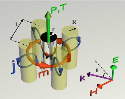
| Figure 1: Visualization of a metamolecule, consisting of a PEC cylinder and four dielectric cylinders around. P stands for electric dipole moment of the conductor and T stands for toroidal moment of the dielectric coating | |
| The aim of the project is to model and then prototype a metamaterial, which will make nano-scale objects invisible in the uncovered THz frequency range. | |
| On the part of Politecnico di Torino, Professor Ladislau Matekovits heads the research group, while Professor Alexey Basharin leads the Russian team. In the research, 4 PhD students and other young professionals are also involved. | |
| A cylinder of perfect electric conductor (PEC) with radius r=2.5 µm has been considered in order to imitate a nano-sensor. Being metallic, it possesses very high wave scattering, allowing to carry out calculations for the maximum possible level of re-radiation. The modeling was performed in THz range, which stands between infrared and microwave bands. | |
| The key element of the new metamaterial is a metamolecule (Fig. 1), consisting of four dielectric lithium tantalate (LiTaO3) cylinders, r=5 µm. Serving as a coating for a nano-sensor, dielectrics interact with radiation, exciting non-radiating anapole mode. Separated from each other, all the elements radiate and distort the electric and magnetic fields (Fig. 2 a, b), but when considered all together the object becomes invisible for an external observer (Fig. 2 c). | |
 |
|
| Figure 2: Visible radiation of elements, where (a) is the central element without coating; (b) is coating elements without a central element; © is metamolecule: central element in the coating. | |
| Apart from the used LiTaO3, depending on the field of application, other materials can be considered. For example, in nano-optics it would be possible to work with silicon and germanium, while in biomedical sensoring biocompatible sodium chloride would be a possible alternative. | |
| The next research stage, which is the experimental characterization of a prototype of the proposed structure in vitro, is scheduled for this autumn. | |
| Concurrently, interests in creating configurations by using proper materials, e.g., graphene, and geometrical arrangements that are only transparent at certain wavelengths and/or angles of incidence are targeted. The challenge set by scientists from Politecnico di Torino and NUST MISIS is to generalize the experience to develop a theory which can be used to model and then assemble metamaterials that will cloak nano-scaled objects at all the wavelengths and at any angles. |
| Source: National University of Science and Technology MISIS |
Folosind valuri de lumină, cercetătorii au arătat că un sistem non-topologic devine topologic atunci când se adaugă o tulburare aleatorie: nici o lumină nu este transmisă prin interiorul structurii, dar lumina curge peste suprafață într-o manieră unidirecțională.
Sistemul topologic fotonic a fost fabricat prin utilizarea impulsurilor laser concentrate cu densități enorme de energie în gama gigawatt, gravarea ghidurilor de undă într-un mediu de sticlă cu silice de înaltă puritate. Ghidurile de undă au fost aranjate într-o structură de tip grafenie în fagure de miere.
Aceste ghiduri de undă paralele, care ghidează lumina ca fibrele de sticlă, sunt în acest caz proiectate nu ca niște linii drepte ci ca linii elicoidale, astfel încât propagarea luminii în direcția înainte corespunde cu un șurub în sensul acelor de ceasornic și în direcția inversă un șurub invers acelor de ceasornic
| Posted: Aug 23, 2018 | |
Added disorder drives transition to photonic topological insulator(Nanowerk News) Research on insulators with topologically protected surface conductivity – in short: topological insulators – is currently in vogue. Topological materials may be able to replace semiconductor technology in the future. |
|
| Topological insulators are characterized by remarkable electrical properties. While these structures have insulating properties in their interior, their conductivity on the surface is extremely robust – to such a degree that in principle an electron current, once introduced, would never cease to flow: one speaks of a „topologically” protected current. Analogous to a stream of electrons, which are half- integer spin particles, so-called fermions, the principle of the topological insulator also works with light particles, so-called bosons, having integer spin. | |
| The properties of a topological insulator are generally stable and persist even when disorder is added. Only a very large disorder in the regular structure can cause the conductive properties on the surface to vanish, resulting in a normal insulator. For photonic topological insulators, this regime of very large disorder means that no light at all can pass through the interior of such a structure, nor can it be transmitted on the surface. | |
| In 2009, Chu, Jain, and Shen theoretically investigated electronic topological insulators with quite extraordinary properties. The starting point of their considerations was a normal insulator, which does not conduct electricity. In their numerical simulation, they showed that the characteristic properties of topological insulators – interior insulation and perfect conductance along the surface (edge) – can be generated by introducing random disorder of the structure. This hypothesis has thus far never been proven in an experiment. | |
 |
|
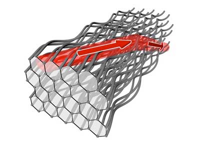
| Fig. 1: A honeycomb waveguide structure with helical waveguides acts as a photonic topological insulator so that light is guided along the surface. | |
| In a paper in Nature („Photonic Topological Anderson Insulators”), this hypothesis for electrons in solids was experimentally demonstrated for light waves by an international team of scientists based at the University of Rostock (Germany), the Technion (Israel), as well as Penn State University and the University of Maryland (U.S.). After extensive theoretical considerations and numerically complex simulations, an experimental design was implemented. | |
| Using light waves, the researchers showed that a non-topological system becomes topological when random disorder is added: no light is transmitted through the interior of the structure, but light flows over the surface in a unidirectional fashion. | |
| The photonic topological system was fabricated by using focused laser pulses with enormous energy densities in the gigawatt range, engraving waveguides into a high-purity fused-silica glass medium. The waveguides were arranged in a honeycomb graphene structure. | |
| These parallel waveguides, which guide the light like glass fibers, are in this case designed not as straight lines but as helical lines, so that the propagation of the light in the forward direction corresponds to a clockwise screw and in the reverse direction a counterclockwise screw. This creates the diffraction properties of a topological insulator, where light circulates around the circumference of the helical array of waveguides in a single direction, and in a way that is immune to disorder such as a missing waveguide (Fig. 1). | |
| However, when the helical honeycomb lattice is systematically modified so that the refractive index of adjacent waveguides is slightly different, the topological properties are destroyed: the light no longer flows on the surface in a unidirectional manner (Fig. 2). When a random disorder is added on top of this modified structure, the topological properties are fully recovered. | |
 |
|
| Fig. 2: Adding further disorders to the refractive indices of the waveguides restores the topological properties so that light flows again along the surface of the structure. | |
| In the experimental setup, light from a red Helium Neon laser is coupled into the waveguide structure. At the other end of the waveguide structure, a camera detects whether light is transmitted through the structure or is transmitted on the surface. In a first experiment, the refractive indices of every adjacent waveguides were made to differ by two ten thousandths. Thus the conductive properties of the topological structure were completely destroyed: no light could be detected behind the structure. But what happens if further disorders are added to the existing disorder? | |
| In a second experiment, the waveguides were prepared in such a way that irregularly distributed differences in the refractive indices of all waveguides were added to the existing regular disorder of adjacent waveguides. Contrary to the expectation that in the event of further disorder in the topological structure the purely insulating properties would be retained and it would remain dark in the sample, the second experiment showed light conduction across the surface. Light could indeed be detected at the edge. | |
| Thus, in the case of light, the experimental proof of the hypothesis of Chu et al., which had originally been expressed only for electrons, has succeeded: by adding disorder, topological insulators can be generated from normal insulators, a highly counterintuitive result. The properties of topological materials as such are quite remarkable; however the dependence of their properties on disorder in the structure is even more extraordinary. | |
| The novel findings of the international research group may contribute to further elucidating the bizarre properties of topological insulators. | |
| “These findings shed new light onto the peculiar properties of topological insulators,” said Professor Alexander Szameit, principal investigator of the Rostock group and lead author of the publication. “This shows that using photonics, we have opened the door to understanding disordered topological insulators in a completely new way. Photonic topological systems could potentially be a route to overcoming parasitic disorder in both fundamental science and real-world applications.” | |
| Professor Mordechai Segev of the Technion added: “The first photonic topological insulator for light was realized in 2013 through collaboration between my group, where the research was led by Mikael Rechtsman and Yonatan Plotnik, and the group of Alex Szameit (at that time in Jena, Germany). Two years later, Mikael Rechtsman and my young colleague Netanel Lindner wrote a theory paper that envisioned the current experiment. And now the experiment has become a reality through the efforts of Alex’s students in a beautiful paper which we all collaborated on. It is fascinating to see how this new field is being led by a group of young, very talented people like Mik, Netanel, Alex and their students, in three different countries.” |
| Source: Universität Rostock |
au arătat cum poate fi proiectat un material feroelectric în așa fel încât pereții domeniului pot fi utilizați pentru a transmite microunde cu un grad mai mare de control al frecvenței decât dispozitivele mobile pe care le folosim în prezent;au simulat comportamentul dinamic la scară atomică a materialului special de film la diferite valori ale temperaturii, tensiunii și câmpului electric, comparându-l cu cel pentru o „perfect” cristal feroelectric fără pereți de domenii – ceea ce a evidențiat comportamentul excepțional al materialului.
| Posted: Aug 21, 2018 | |
Once a performance barrier, material quirk could improve telecommunications(Nanowerk News) Researchers who study and manipulate the behavior of materials at the atomic level have discovered a way to make a thin material that enhances the flow of microwave energy. The advance, which could improve telecommunications, sheds new light on structural traits, generally viewed as static and a hindrance, that, when made to be dynamic, are actually key to the material’s special ability. |
|
| The discovery, reported in the journal Nature („Resonant domain-wall-enhanced tunable microwave ferroelectrics”), shows how domain walls – the naturally occurring boundaries, separating atoms with different directions of relative displacement, that create dipoles within a material – could actually be an entryway for accessing a much wider range of electromagnetic frequencies. And this access could one day expand the range of frequencies used as communications channels. | |
 |
|
| Artist’s top-view rendering of a domain wall-variant material featuring a diffuse boundary separating aligned-dipole regions in a ferroelectric crystal film. Tunable, resonant fluctuations of these two-dimensional defects enable reduction of microwave radio frequency dielectric losses to beyond the crystal’s intrinsic limit. (Image: Drexel University) | |
| In the paper, researchers from Drexel University, Bar-Ilan University in Israel, the University of California at Berkeley, the University of California at Santa Barbara, the Carnegie Institution for Science, and the University of Pennsylvania showed how a ferroelectric material can be designed in such a way that domain walls can be used to transmit microwaves with a higher degree of frequency control than the mobile devices we currently use. | |
| „As consumer demand for mobile communications increases the available wireless spectrum is increasingly congested and new technologies are needed to create adaptive, frequency-agile antennas,” said Robert York, a professor at UC Santa Barbara and a co-author of the paper. „Tunable dielectric materials could be a potential solution.” | |
| Using the domain walls within a material to enhance its transmission quality is a particularly unexpected approach because the presence of these boundaries tends to strongly diminish a material’s ability to pass a microwave electromagnetic field. Until now, the best film materials for transmitting electromagnetic fields in radio-frequency devices were generally considered to be single-crystal materials that do not have any permanent dipole moments – let alone domain walls. | |
| But the research team turned this perception of domain walls on its head by creating a ferroelectric material with a high density of domain walls, that can outperform single crystals when it comes to tunability and transmission quality. | |
| The group found that the domain walls of a thin film of barium strontium titanate, a frequently studied ferroelectric material, function like vibrating guitar strings that resonate together. Rather than absorbing or scattering microwaves, the presence of a dense, but ordered, thicket of oscillating domain walls actually improves the quality of the transmission. | |
| „Even the best-quality bulk single crystals, without permanent, re-orientable dipoles, have higher losses at higher frequencies, due to interference caused by the vibrations of atoms in the lattice,” said Jonathan Spanier, a materials science professor at Drexel who led the research. „Film materials with permanent dipoles form domain walls, and the loss is much worse. But films that support reversible domain wall motion and their oscillating behavior surprisingly break that trend and resonate over a wide range of frequencies.” | |
| According to the researchers, „the proximity of and accessibility among thermodynamically predicted strain-induced, ferroelectric domain wall variants to achieve gigahertz microwave tunability and dielectric loss that surpass those for the current best film devices by 1-2 orders of magnitude, attaining values comparable to bulk single crystals, but in an intrinsically tunable material,” they write in the paper. | |
| The key to this exceptional tunability, according to co-author Zongquan Gu, a postdoctoral scientist in Spanier’s research group, is the abundance of different phases, „the ferroelectric phase transition temperature marks the onset of the permanent dipolar ordering. A peak in the dielectric susceptibility, a thermodynamic property related to the magnitude of capacitance, is a hallmark of the transition,” Gu said. „Engineering a film material to have many, more easily available ‘phases’ near the transition allows the material to attain much higher capacitance tuning with the same voltage.” | |
| Along with Spanier, Gu, and Geoffrey Xiao, an undergraduate student at Drexel, launched theory and simulation efforts for the prediction of domain wall-rich energy landscapes to direct the production of the domain wall-rich barium strontium titanate film. With Spanier’s colleagues at Berkeley, led by Lane Martin, professor in materials science, a leader in ferroelectric domain walls film science, Gu also made and characterized the first samples of the material, using a process called strain engineering to create a dense concentration of domain walls. | |
| From there, collaborators from Bar-Ilan University in Israel led by Ilya Grinberg, a professor of chemistry, simulated the atomic-scale dynamic behavior of the special film material at different values of temperature, strain and electric field, comparing it with that for a „perfect” ferroelectric crystal without any domain walls – which revealed the material’s exceptional behavior. | |
| This intrinsic tunability, meaning the material’s excellent transmission abilities do not require any external, electromechanical enhancement, make it promising for use in communication devices – where efficient access to spectrum is essential. | |
| At UC Santa Barbara, York, a professor of electrical and computer engineering, and his doctoral student Cedric Meyers, fabricated electrode test structures that enabled the measurement and analysis of material’s resonant microwave response, including its tunability. | |
| „Tunable dielectric materials have been a focus of investigation in my group at UCSB since the late 1990s,” York said. „But despite some progress early on, we consistently ran up against limitations of the materials that were poorly understood. This work helps to better understand these limitations and to identify potential solutions.” |
| Source: Drexel University |
Aceste progrese, făcute de mediul colaborativ al platformei Grafene, ar putea conduce la aplicații promițătoare în senzori, în optoelectronică și în dispozitive flexibile. Cercetătorii visează acum dispozitive hibride multifuncționale de înaltă performanță sub controlul celei mai abundente și puternice surse de lumină energetică a naturii.Această moleculă – un spiropyran capabil să poată fi redată prin imagine – poate fi apoi ancorată la suprafața materialelor cum ar fi grafenul sau disulfura de molibden, generând astfel o superlattică macroscopică hibridă precis atomică. Când este iluminat, întreaga structură supramoleculară are o rearanjare structurală colectivă, care poate fi vizualizată direct cu o rezoluție sub-nanometrică prin scanarea microscopiei de tunel.
| Posted: Aug 14, 2018 | |
Flipping the switch on supramolecular electronics(Nanowerk News) Graphene and related materials hold great potential for technological applications such as electronics, sensors, and energy storage devices, among others. Thanks to their high surface sensitivity, these materials are an ideal platform to study the interplay between molecular assemblies at the nanoscale and macroscopic electrical phenomena. |
|
| Researchers within the Graphene Flagship designed a molecule that can reversibly undergo chemical transformations when illuminated with ultraviolet and visible light (Nature Communications, „Collective molecular switching in hybrid superlattices for light-modulated two-dimensional electronics”). | |
| This molecule – a photoswitchable spiropyran – can be then anchored to the surface of materials such as graphene or molybdenum disulfide, thus generating an atomically precise hybrid macroscopic superlattice. When illuminated, the whole supramolecular structure experiences a collective structural rearrangement, which could be directly visualized with a sub-nanometer resolution by scanning tunneling microscopy. | |
| More importantly, this light-induced reorganization at the molecular level induces large changes in the macroscopic electrical properties of the hybrid devices. The molecules, together with the layers of graphene and related materials, can convert single-molecule events into a spatially homogeneous switching action that generates a macroscopic electrical response. This novel and versatile approach takes supramolecular electronics to the next level. | |
 |
|
| Photo-switchable molecular crystals in two dimensions. (click on image to enlarge) | |
| ‘Thanks to this new approach, we can exploit the capacity of collective switching events occurring in superlattices of photochromic molecules assembled onto graphene and related materials to induce large scale and reversible modulation in the electrical properties of high-performance opto-electronic devices,’ explains Paolo Samorì, lead author of the paper. ‘This technology could find applications in the next generation of smart and portable electronics, with programmable properties,’ he adds. | |
| Samorì also explains how this idea of tailoring molecular superlattices could generate a wide variety of new materials with tunable and responsive properties. ‘To dial your functions! You only need to carefully choose the right molecules, the thus-formed superlattice will allow to maximize the change in properties as a response to external inputs,’ he says. | |
| Vittorio Pellegrini, researcher at IIT and Division Leader for Energy, Composites, and Production at the Graphene Flagship, highlights how the research is ‘unique in the way it combines graphene and other related materials with light-responsive chemical molecules. These macroscopic arrangements are promising platforms for optoelectronics.’ Pellegrini points out the outstanding potential of these new findings: ‘the molecular ultra-thin coating can be tailored just by synthesizing different molecules.’ Moreover, ‘this discovery will lead us to the development of devices, as the technique developed by Samorì and his team can be scaled up in reproducible manner,’ he added. Samorì agrees: ‘The limit in the scalability is the accessibility to ultra-flat and atomically precise graphene and related materials.’ | |
| These advances, made possible by the collaborative environment of the Graphene Flagship, could lead to promising applications in sensors, optoelectronics, and flexible devices. Researchers now dream of high-performance multifunctional hybrid devices under control of nature’s most abundant and powerful source of energy – light. | |
| Professor Andrea C. Ferrari, Science and Technology Officer of the Graphene Flagship, and Chair of its management panel added: ‘Supra-molecular chemistry has been part of the Flagship research since the very beginning. Over the years our partners have improved and developed the techniques that enable to interface molecules with graphene and related materials. We are now witnessing a steady progress towards applications, as shown by this interesting work.’ |
| Source: Graphene Flagship |
Un material care constă în atomi dintr-un singur element, dar are proprietăți complet diferite în funcție de aranjamentul atomic – acest lucru poate părea ciudat, dar este de fapt realitate cu nano-panglici graphene. Panglicile, care au doar câțiva atomi de carbon și un singur atom gros, au proprietăți electronice foarte diferite, în funcție de forma și lățimea lor: conductor, semiconductor sau izolator.
| Posted: Aug 09, 2018 | |
Quantum chains in graphene nanoribbons(Nanowerk News) Empa researchers, together with researchers from the Max Planck Institute for Polymer Research in Mainz and other partners, have achieved a breakthrough that could in future be used for precise nanotransistors or – in the distant future – possibly even quantum computers, as the team reports in the current issue of the scientific journal Nature („Engineering of robust topological quantum phases in graphene nanoribbons”). |
|
 |
|
| When graphene nanoribbons contain sections of varying width, very robust new quantum states can be created in the transition zone. | |
| A material that consists of atoms of a single element, but has completely different properties depending on the atomic arrangement – this may sound strange, but is actually reality with graphene nano-ribbons. The ribbons, which are only a few carbon atoms wide and exactly one atom thick, have very different electronic properties depending on their shape and width: conductor, semiconductor or insulator. | |
| An international research team led by Empa’s „nanotech@surfaces” laboratory has now suc-ceeded in precisely adjusting the properties of the ribbons by specifically varying their shape. The particular feature of this technology is that not only can the „usual” electronic properties mentioned above be varied – it can also be used to generate specific local quantum states. | |
| So what’s behind it? If the width of a narrow graphene nanoribbon changes, in this case from seven to nine atoms, a special zone is created at the transition: because the electronic properties of the two areas differ in a special, so-called topological way, a „protected” and thus very robust new quantum state is created in the transition zone. This local electronic quantum state can now be used as a basic component to produce tailor-made semiconductors, metals or insulators – and possibly even as a component in quantum computers. | |
| The Empa researchers under the lead of Oliver Gröning were able to show that if these ribbons are built with regularly alternating zones of different widths, a chain of interlinked quantum states with its own electronic structure is created by the numerous transitions. The exciting thing is that the electronic properties of the chain change depending on the width of the different segments. This allows them to be finely adjusted – from conductors to semiconductors with different bandgaps. This principle can be applied to many different types of transition zones – for example, from seven to eleven atoms. | |
| „The importance of this development is also underlined by the fact that a research group at the University of California, Berkeley, came to similar results independently of us,” said Gröning. The work of the US research team has been published in the same issue of Nature . | |
On the way to nanoelectronics |
|
| Based on these novel quantum chains, precise nano-transistors could be manufactured in the future – a fundamental step on the way to nanoelectronics. Whether the switching distance between the „1” state and the „0” state of the nanotransistor is actually large enough depends on the bandgap of the semiconductor – and with the new method this can be set almost at will. | |
 |
|
| The electronic properties of the chain can be finely adjusted. | |
| In reality, however, this is not quite as simple: for the chain to have the desired electronic properties, each of the several hundred or even thousands of atoms must be in the right place. | |
| „This is based on complex, interdisciplinary research, ” says Empa researcher Gröning. „Researchers from different disciplines in Dübendorf, Mainz, Dresden, and Troy (USA) worked together – from theoretical understanding and specific knowledge of how precursor molecules have to be built and how structures on surfaces can be selectively grown to structural and electronic analysis using a scanning tunneling microscope.” | |
An excursion into the quantum realm |
|
| Ultrasmall transistors – and thus the next step in the further miniaturization of electronic circuits – are the obvious application possibilities here: although they are technically challenging, electronics based on nanotransistors actually work fundamentally the same as today’s microelectronics. | |
| The semiconducting nanoribbons produced by the Empa researchers would allow transistors with a channel cross-section 1,000 times smaller than typically manufactured today. However, further possibilities can also be imagined, for example in the field of spintronics or even quantum informatics. | |
 |
|
| Top: Schematic representation of the production of hybrid nanobands using two different precursor molecules. The left (small) produces a smooth 7-carbon atom wide nanoband. The larger one produces a 7-11 atom wide, caroform segment. Atomic force microscopy: Atomic force microscope image of a hybrid graphene nanoband with 5 „diamond” segments (7-11 segments) in the middle which is continued left and right by smooth 7-nanobands. The black scale bar is 1 nm long. Scanning tunnel spectroscopy: Spectroscopic image of the localized quantum states (bright regions) at both ends of the diamond region. The section corresponds to that of the atomic force microscope image. Simulation of the scanning tunnel spectroscopy: Theoretical prediction of how the quantum states to be expected at the end of the diamond segment should look in the experiment. | |
| This is because the electronic quantum states at junctions of graphene nanoribbons of different widths can also carry a magnetic moment. This could make it possible to process information not by charge as was previously customary, but by the so-called spin – in the figurative sense the „direction of rota-tion” of the state. And the development could even go one step further. | |
| „We have observed that topological end states occur at the ends of certain quantum chains. This offers the possibility of using them as elements of so-called qubits – the complex, interlocked states in a quantum computer,” explains Oliver Gröning. | |
| Today and tomorrow, however, no quantum computer is built from nanoribbons – there is still a lot of research needed, says Gröning: „The possibility of flexibly adjusting the electronic properties through the targeted combination of individual quantum states represents a major leap for us in the production of new materials for ultra-miniaturized transistors.” | |
| The fact that these materials are stable under environmental conditions plays an important role in the development of future applications. | |
| „The further-reaching potential of the chains to create local quantum states and link them together in a targeted manner is also fascinating,” Gröning continues. „Whether this potential can actually be exploited for future quantum computers remains to be seen, however. It is not enough to create localized topological states in the nanoribbons – these would also have to be coupled with other materials such as superconductors in such a way that the conditions for qubits are actually met.” |
| Source: Empa |
creat materiale care pot stoca energie în acest fel, pot fi stoarse în mod repetat, fără a se deteriora și chiar schimba forma, dacă este necesar.
Aceste tipuri de materiale sunt numite auxetice și se comportă destul de diferit de cele obișnuite. În loc să se stingă atunci când sunt stoarse, se prăbușesc în toate direcțiile, stocând energia din interior.
| Posted: Aug 09, 2018 | |
Scientists design material that can store energy like an eagle’s grip(Nanowerk News) What do a flea and an eagle have in common? They can store energy in their feet without having to continuously contract their muscles to then jump high or hold on to prey. Now scientists at Queen Mary University of London and University of Cambridge have created materials that can store energy this way, be squeezed repeatedly without damage, and even change shape if necessary. |
|
| These kinds of materials are called auxetics and behave quite differently from regular materials. Instead of bulging out when squeezed, they collapse in all directions, storing the energy inside. | |
| Current auxetic material designs have sharp corners which enable them to fold onto themselves, achieving higher density. This is a property that has been recognised recently in lightweight armour designs, where the material can collapse in front of a bullet upon impact. This is important because mass in front of a bullet is the biggest factor in armour effectiveness. | |
| The sharp corners also concentrate forces and cause the material to fracture if squeezed multiple times, which is not a problem for armour as it is only designed to be used once. | |
| In this study, published in Frontiers in Materials („Low Fatigue Dynamic Auxetic Lattices with 3D Printable, Multistable, and Tuneable Unit Cells”), the team of scientists redesigned the materials with smooth curves which distribute the forces and make repeated deformations possible for other applications where energy storing and shape-changing material properties are required. | |
 |
|
| The ratcheting building block that could be embedded in the new materials. After vertical compression, it keeps materials collapsed, and can release their energy on side-ways pull. (click on image to enlarge) | |
| The work lays the basis for designs of lightweight 3D supports, which also fold in specific ways and store energy which could be released on demand. | |
| Principle investigator Dr Stoyan Smoukov, from Queen Mary University of London, said: “The exciting future of new materials designs is that they can start replacing devices and robots. All the smart functionality is embedded in the material, for example the repeated ability to latch onto objects the way eagles latch onto prey, and keep a vice-like grip without spending any more force or effort.” | |
| The team expects its nature-inspired designs could be used in energy-efficient gripping tools required in industry, re-configurable shape-on-demand materials, and even lattices with unique thermal expansion behaviour. | |
| Eesha Khare, a visiting undergraduate student from Harvard University who was instrumental in defining the project, added: “A major problem for materials exposed to harsh conditions, such as high temperature, is their expansion. A material could now be designed so its expansion properties continuously vary to match a gradient of temperature farther and closer to a heat source. This way, it will be able to adjust itself naturally to repeated and severe changes.” | |
| The flexible auxetic material designs, which were not possible before, were adapted specifically to be easily 3D-printed, a feature the authors consider essential. | |
| Dr Smoukov added: “By growing things layer-by-layer from the bottom up, the possible material structures are mostly limited by imagination, and we can easily take advantage of inspirations we get from nature.” |
| Source: Queen Mary University London |