Oamenii de știință creează biobaterite biodegradabile, pe bază de hârtie(Scientists create biodegradable, paper-based biobatteries)

Bateriile viitorului pot fi făcute din hârtie. Cercetătorii de la Universitatea Binghamton, Universitatea de Stat din New York, au creat o baterie biodegradabilă, pe bază de hârtie, care este mai eficientă decât era posibil anterior.anterior”.
Biobatteria folosește un hibrid de polimeri de hârtie și de inginerie. Polimerii – acidul poli (amic) și poli (dianhidrida piromelit-p-fenilendiamină) – au fost cheia pentru a da proprietăților biodegradabile ale bateriilor.

Posted: Aug 08, 2018

Scientists create biodegradable, paper-based biobatteries

(Nanowerk News) The batteries of the future may be made out of paper. Researchers at Binghamton University, State University at New York have created a biodegradable, paper-based battery that is more efficient than previously possible (Advanced Sustainable Systems, „Green Biobatteries: Hybrid Paper–Polymer Microbial Fuel Cells”).

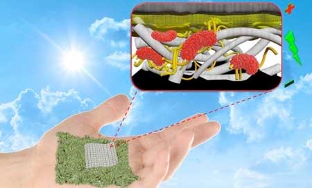
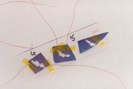
paper-based battery
Researchers at Binghamton University, State University at New York have created a biodegradable, paper-based battery that is more efficient than previously possible. (Image: Seokheun “Sean” Choi)
For years, there has been excitement in the scientific community about the possibility of paper-based batteries as an eco-friendly alternative. However, the proposed designs were never quite powerful enough, they were difficult to produce and it was questionable whether they were really biodegradable.
This new design solves all of those problems.
Associate Professor Seokheun “Sean” Choi from the Electrical and Computer Engineering Department and Professor Omowunmi Sadik from the Chemistry Department worked on the project together. Choi engineered the design of the paper-based battery, while Sadik was able to make the battery a self-sustaining biobattery.
“There’s been a dramatic increase in electronic waste and this may be an excellent way to start reducing that,” said Choi. “Our hybrid paper battery exhibited a much higher power-to-cost ratio than all previously reported paper-based microbial batteries.”
The biobattery uses a hybrid of paper and engineered polymers. The polymers – poly (amic) acid and poly (pyromellitic dianhydride-p-phenylenediamine) – were the key to giving the batteries biodegrading properties.
The team tested the degradation of the battery in water and it clearly biodegraded without the requirements of special facilities, conditions or introduction of other microorganisms.
The polymer-paper structures are lightweight, low-cost and flexible. Choi said that flexibility also provides another benefit.
“Power enhancement can be potentially achieved by simply folding or stacking the hybrid, flexible paper-polymer devices,” said Choi.
The team said that producing the biobatteries is a fairly straightforward process and that the material allows for modifications depending on what configuration is needed.
Source: University of Binghamton

Filme transparente, conductive, promițătoare pentru dezvoltarea unor ecrane flexibile (Transparent, conductive films promising for developing flexible screens)

Cercetătorii au demonstrat fabricarea pe scară largă a unui nou tip de peliculă electrozică transparentă pe bază de argint nanopatternat. Ecranele tactile cu ecran tactil și televizoarele cu ecran plat utilizează electrozi transparenți pentru a detecta atingerea și pentru a comuta rapid culoarea fiecărui pixe; cercetătorii raportează fabricarea unui film subțire transmițător transparent pe discuri de sticlă cu diametrul de 10 centimetri. Pe baza estimărilor teoretice care se potrivesc îndeaproape cu măsurătorile experimentale, ele calculează că electrozii subțiri de film subțire pot funcționa semnificativ mai bine decât cei utilizați pentru afișajele flexibile existente și ecranele touch.

Posted: Jun 07, 2018

Transparent, conductive films promising for developing flexible screens

(Nanowerk News) Researchers have demonstrated large-scale fabrication of a new type of transparent conductive electrode film based on nanopatterned silver. Smartphone touch screens and flat panel televisions use transparent electrodes to detect touch and to quickly switch the color of each pixel. Because silver is less brittle and more chemically resistant than materials currently used to make these electrodes, the new films could offer a high-performance and long-lasting option for use with flexible screens and electronics. The silver-based films could also enable flexible solar cells for installation on windows, roofs and even personal devices.

In the journal Optical Materials Express („Transparent and conductive electrodes by large-scale nano-structuring of noble metal thin-films”), the researchers report fabrication of a transparent conducting thin-film on glass discs 10 centimeters in diameter. Based on theoretical estimations that matched closely with experimental measurements, they calculate that the thin-film electrodes could perform significantly better than those used for existing flexible displays and touch screens.
Nanopatterned Thin-Film Illustration
The researchers used an approach called colloidal lithography to create a silver nanopattern that conducts electricity while letting light through the holes. The new transparent electrode films could be useful for solar cells as well as flexible displays and touch screens. (Image: Jes Linnet, University of Southern Denmark)
„The approach we used for fabrication is highly reproducible and creates a chemically stable configuration with a tunable tradeoff between transparency and conductive properties,” said the paper’s first author, Jes Linnet from the University of Southern Denmark. „This means that if a device needs higher transparency but less conductivity, the film can be made to accommodate by changing the thickness of the film.”

Finding a flexible alternative

Most of today’s transparent electrodes are made of indium tin oxide (ITO), which can exhibit up to 92 percent transparency – comparable to glass. Although highly transparent, ITO thin films must be processed carefully to achieve reproducible performance and are too brittle to use with flexible electronics or displays. Researchers are seeking alternatives to ITO because of these drawbacks.
The anti-corrosive nature of noble metals such as gold, silver and platinum makes them promising ITO alternatives for creating long-lasting, chemically resistant electrodes that could be used with flexible substrates. However, until now, noble metal transparent conductive films have suffered from high surface roughness, which can degrade performance because the interface between the film and other layers isn’t flat.
Silver Thin-Film with Particles
This scanning electron microscopy image shows a thin film of silver deposited over plastic nanoparticles. Dissolving the particles leaves a precise pattern of honeycomb-like holes that allow light to pass through, producing an electrically conductive and optically transparent film. (Image: Jes Linnet, University of Southern Denmark)
Transparent conductive films can also be made using carbon nanotubes, but these films don’t currently exhibit high enough conductance for all applications and tend to also suffer from surface roughness due to the nanotubes stacking on top of each other.
In the new study, the researchers used an approach called colloidal lithography to create transparent conductive silver thin films. They first created a masking layer, or template, by coating a 10-centimeter wafer with a single layer of evenly sized, close-packed plastic nanoparticles. The researchers placed these coated wafers into a plasma oven to shrink the size of all the particles evenly. When they deposited a thin film of silver onto the masking layer, the silver entered the spaces between the particles. They then dissolved the particles, leaving a precise pattern of honeycomb-like holes that allow light to pass through, producing an electrically conductive and optically transparent film.

Balancing transparency and conductivity

The researchers demonstrated that their large-scale fabrication method can be used to create silver transparent electrodes with as much as 80 percent transmittance while keeping electrical sheet resistance below 10 ohms per square – about a tenth of what has been reported for carbon-nanotube-based films with the equivalent transparency. The lower the electrical resistance, the better the electrodes are at conducting an electrical charge.
colloidal lithography fabrication process
The researchers used colloidal lithography was used to create a thin film that was transparent and conductive thin film. (a) Schematic illustration of the fabrication process. (b) A single nanohole after the silver was deposited deposition and dissolving of the plastic particle. Scale bar: 200 nm. (c) Low magnification micrograph of deposited silver thin-film on homogenous particle monolayer, demonstrating large-scale feasibility. Scale bar: 50 microns. (d) Particle monolayer on substrate after spin-coating and a short (60 s) time in the plasma oven: Scale bar: 2 microns. (e) Particle monolayer after a long (3 min) time in the plasma oven, demonstrating that original particle positions are preserved even after significant size reduction. Scale bar: 10 microns. (Image: Jes Linnet, University of Southern Denmark) (click on image to enlarge)
„The most novel aspect of our work is that we accounted for both the transmission properties and the conductance properties of this thin film using theoretical analysis that correlated well with measured results,” said Linnet. „Fabrication problems typically make it hard to get the best theoretical performance from a new material. We decided to report what we encountered experimentally and postulate remedies so that this information could be used in the future to avoid or minimize problems that may affect performance.”
The researchers say that their findings show that colloidal lithography can be used to fabricate transparent conductive thin films that are chemically stable and could be useful for a variety of applications.
Source: The Optical Society

Puzzle cu graphene foto excitat rezolvat(Photoexcited graphene puzzle solved)

Folosirea grafenului ca material sensibil la lumină pentru detectoarele de lumină poate oferi îmbunătățiri semnificative în ceea ce privește materialele folosite în zilele noastre.
De exemplu, grafenul poate detecta lumina de aproape orice culoare și dă un răspuns electronic extrem de rapid, într-o singură milionime dintr-o milionă de secundă. Astfel, pentru a proiecta corect detectorii de lumină pe bază de grafen, este esențial să înțelegem procesele care au loc în interiorul grafenului după ce absoarbe lumina.

Posted: Jun 01, 2018

Photoexcited graphene puzzle solved

(Nanowerk News) Light detection and control lies at the heart of many modern device applications, such as smartphone cameras. Using graphene as a light-sensitive material for light detectors can offer significant improvements with respect to materials being used nowadays.

For example, graphene can detect light of almost any color, and it gives an extremely fast electronic response within one millionth of a millionth of a second. Thus, in order to properly design graphene-based light detectors it is crucial to understand the processes that take place inside the graphene after it absorbs light.
The Mainz-based researchers Dr. Hai Wang, Professor Dmitry Turchinovich, Professor Mathias Kläui, and Professor Mischa Bonn, in collaboration with scientists from various European labs, have now succeeded in understanding these processes. The project was led by Dr. Klaas-Jan Tielrooij from ICFO in Spain, who was recently elected visiting professor at the Materials Science in Mainz (MAINZ) Graduate School of Excellence.
ultrafast optical pump
Schematic representation of the ultrafast optical pump – terahertz probe experiment, where the optical pump induces electron heating and the terahertz pulse is sensitive to the conductivity of graphene directly after this heating process. (Image: Fabien Vialla)
Published recently in Science Advances („The ultrafast dynamics and conductivity of photoexcited graphene at different Fermi energies”), their work gives a thorough explanation of why the graphene conductivity in some cases increases after light absorption while it decreases in others.
The researchers were able to show that this behavior correlates with the way in which the energy from the absorbed light flows to the graphene electrons: After light is absorbed by the graphene, the processes through which graphene electrons heat up happen extremely fast and with a very high efficiency.
For highly doped graphene with many free electrons present, ultrafast electron heating leads to carriers with elevated energy, so-called hot carriers. This, in turn, leads to a decrease in conductivity. Interestingly enough, for weakly doped graphene with less free electrons, electron heating leads to the creation of additional free electrons and, thus, an increase in conductivity. These additional carriers are the direct result of the gapless nature of graphene. In gapped materials, electron heating does not lead to additional free carriers.
This simple scenario of light-induced electron heating in graphene can explain many observed effects. Aside from describing the conductive properties of the material after light absorption, it can explain carrier multiplication, where under specific conditions one absorbed light particle, i.e., a photon, can indirectly generate more than one additional free electron and thus create an efficient photo response within a device.
The results of the paper and, in particular, understanding electron heating processes accurately, will definitely mean a great boost in the design and development of graphene-based light detection technology.
Source: Johannes Gutenberg University Mainz

Izolatori noi cu muchii de conducere(Novel insulators with conducting edges)

Clasa nouă de materiale: Izolatori topologici de înaltă calitate;o nouă clasă de izolatori topologici care au proprietăți de conducere pe marginea cristalelor, mai degrabă decât pe suprafața lor;Cercetatorii spera ca in viitor nanofirele fabricate din izolatii topologice de ordin superior pot fi folosite ca trasee de conducere in circuitele electrice. Acestea ar putea fi combinate cu materiale magnetice și superconductoare și utilizate pentru construirea calculatoarelor cuantice.

Posted: Jun 01, 2018

Novel insulators with conducting edges

(Nanowerk News) Topology examines the properties of objects and solids that are protected against perturbations and deformations. Materials known so far include topological insulators, which are crystals that insulate on the inside but conduct electrical current on their surface. The conducting surfaces are topologically protected, which means that they cannot easily be brought into an insulating state.

New class of materials: Higher-order topological insulators

Theoretical physicists at the University of Zurich have now predicted a new class of topological insulators that have conducting properties on the edges of crystals rather than on their surface.
The research team, made up of scientists from UZH, Princeton University, the Donostia International Physics Center and the Max Planck Institute of Microstructure Physics in Halle, dubbed the new material class „higher-order topological insulators” (Science Advances, „Higher-order topological insulators”).
This is a schematic of a higher-order topological insulator in the shape of a nanowire, with conducting channels on its edges.
This is a schematic of a higher-order topological insulator in the shape of a nanowire, with conducting channels on its edges. (Image: University of Zurich)
The extraordinary robustness of the conducting edges makes them particularly interesting: The current of topological electrons cannot be stopped by disorder or impurities. If an imperfection gets in the way of the current, it simply flows around the impurity.

Like a highway for electrons

In addition, the crystal edges do not have to be specially prepared to conduct electrical current. If the crystal breaks, the new edges automatically also conduct current.
„The most exciting aspect is that electricity can at least in theory be conducted without any dissipation,” says Titus Neupert, professor at the Department of Physics at UZH. „You could think of the crystal edges as a kind of highway for electrons. They can’t simply make a U-turn.”
This property of dissipationless conductance, otherwise known from superconductors at low temperatures, is not shared with the previously known topological insulator crystals that have conducting surfaces, but is specific to the higher-order topological crystals.

Further theoretical and experimental research needed

The physicists’ study still mostly relies on theoretical aspects. They have proposed tin telluride as the first compound to show these novel properties. „More material candidates have to be identified and probed in experiments,” says Neupert.
The researchers hope that in the future nanowires made of higher-order topological insulators may be used as conducting paths in electric circuits. They could be combined with magnetic and superconducting materials and used for building quantum computers.
Source: University of Zurich

Izolator-metal de tranziție la scara nanometrica(Insulator-metal transition at the nanoscale)

Dioxidul de vanadiu (VO 2 ) este un astfel de material. Se poate trece de la o fază izolatoare la o fază metalică chiar deasupra temperaturii camerei, o caracteristică exploatată deja pentru senzori.Privind materialul cu o rezoluție de 50 nm, oamenii de știință au putut observa că defectele din material au jucat un rol important în inițierea tranziției de fază de la izolator la metal. Cu toate acestea, mai important, autorii au observat de asemenea o a treia stare intermediară formată în timpul transformării de fază.

Posted: May 30, 2018

Insulator-metal transition at the nanoscale

(Nanowerk News) Controlling the flow of electrons within circuits is how electronic devices work. This is achieved through the appropriate choice of materials. Metals allow electrons to flow freely and insulators prevent conduction. In general, the electrical properties of a material are determined when the material is fabricated and cannot be changed afterwards without changing the material.

However, there are materials that can exhibit metal or insulator behaviour depending on their temperature. Being able switch their properties, these materials could lead to a new generation of electronic devices.
Vanadium Dioxide (VO2) is one such material. It can switch from an insulating phase to a metallic phase just above room temperature, a feature exploited already for sensors. However, the reason why the properties of this material change so dramatically has been a matter of scientific debate for over 50 years.
One of the challenges in understanding why and how this switch occurs is due to a process called phase separation. The insulator-metal phase transition is similar to the ice to liquid transition in water. When ice melts, both liquid and solid water can coexist in separate regions.
Similarly, in VO2, insulating and metallic regions of the material can be coexisting at the same time during the transition. But unlike water, where the different regions are often large enough to see with the naked eye, in VO2 this separation occurs on the nanoscale and it is thus challenging to observe.
As a result, it has been hard to know if the true properties of each phase, or the mixture of both phases, are being measured.
X-rays are a key tool for understanding the properties of materials, but it has been hard to use them to probe materials on the nanoscale because it is hard to build lenses for microscopes that can detect them.
However, in a recent study published in Nano Letters („Imaging Nanometer Phase Coexistence at Defects During the Insulator–Metal Phase Transformation in VO2 Thin Films by Resonant Soft X-ray Holography”), a team of researchers from ICFO and ALBA in Barcelona, the Technisch Universitat and Max-Born Institute in Berlin, and Vanderbilt University in Tennessee, has finally been able to probe the phase transitions that occur in thin films of VO2 using resonant soft X-ray holography.
This technique is capable of imaging the electronic and structural changes in this material with an unprecedented resolution at the nanoscale without the need of a lens.
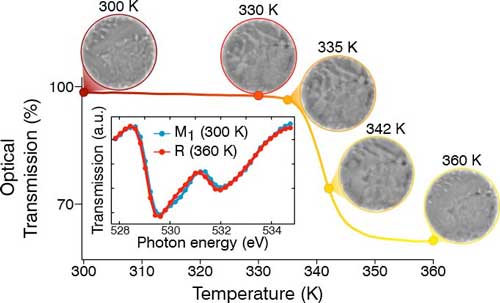
Phase Transition from Insulator to Metallic Phase in VO2 as a Function of the Temperature
Phase transition from insulator to metallic phase in VO2 as a function of the temperature. (Image: ICFO)
By looking at the material with 50 nm resolution, the scientists were able to observe that defects in the material played an important role in initiating the phase transition from the insulator to the metal. However, more importantly, the authors also observed a third intermediate state formed during the phase transformation.
Whilst some regions transformed directly from the insulating to metallic phase, others transformed into a second different insulating state before becoming metallic at higher temperatures with the exact pathway taken depending on the defects present in the material.
The coexistences of three phases has radically changed the views of previous studies that assumed the presence of only two states during the transition. Even more, the study presents new ways in which the transition could be controlled.
In addition to the results obtained on the phase transition in VO2, the work also highlights the possibilities that X-ray holography can bring for studying materials on the nanoscale.
The technique is the only method that can image real-time nanoscale dynamics and is now being used to study the properties of other intriguing materials such as high temperature superconductors.
Source: The Institute of Photonic Sciences (ICFO)

Construcția de nanomateriale pentru calculul de ultimă generație(Building nanomaterials for next-generation computing)

Nanoscientii de la Universitatea Northwestern au dezvoltat un plan pentru fabricarea de noi heterostructuri din diferite tipuri de materiale 2-D. Materialele 2-D sunt straturi individuale de atomi care pot fi stivuite împreună ca „blocuri de construcție nano-interblocate”. Materialele de știință și fizicienii sunt încântați de proprietățile materialelor 2-D și de aplicațiile lor potențiale.

Posted: May 30, 2018

Building nanomaterials for next-generation computing

(Nanowerk News) Nanoscientists at Northwestern University have developed a blueprint to fabricate new heterostructures from different types of 2-D materials. 2-D materials are single atom layers that can be stacked together like “nano-interlocking building blocks.” Materials scientists and physicists are excited about the properties of 2-D materials and their potential applications. The researchers describe their blueprint in the Journal of Applied Physics(„Controlled synthesis of 2D MX2 (M=Mo, W; X=S, Se) heterostructures and alloys”).

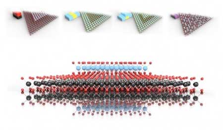
nanoheterostructures using 2-D materials
Top: Vertical MoSe2-WSe2 heterostructure, radial MoS2-WS2 heterostructure, hybrid MoS2-WS2heterostructure and MoSe2-WSe2 alloy building block representations and crystal structure models; Bottom: Vertical MoSe2-WSe2 heterostructure crystal structure model(Image: Cain, Hanson and Dravid)
“We’ve outlined an easy, deterministic and readily deployable way to stack and stitch these individual layers into orders not seen in nature,” said Jeffrey Cain, an author on the paper who was formerly at Northwestern University but is now at Lawrence Berkeley National Laboratory and the University of California.
Cain explained that for nanoscientists, “the dream” is to combine 2-D materials in any order and collate a library of these heterostructures with their documented properties. Scientists can then select appropriate heterostructures from the library for their desired applications. For instance, the computer industry is trying to make transistors smaller and faster to increase computing power. A nanoscale semiconductor with favorable electronic properties could be used to make transistors in next-generation computers.
So far, nanoscientists have lacked clear methods for fabricating heterostructures, and have not yet been able to develop this library. In this work, the scientists looked to solve these fabrication issues. After identifying trends in the literature, they tested different conditions to map out the different parameters required to grow specific heterostructures from four types of 2-D materials: molybdenum disulfide and diselenide, and tungsten disulfide and diselenide. To fully characterize the atomically thin final products, the scientists used microscopy and spectrometry techniques.
The group was inspired by the science of time-temperature-transformation diagrams in classical materials, which maps out heating and cooling profiles to generate precise metallic microstructures. Based on this method, the researchers packaged their findings into one diagrammatic technique – the Time-Temperature-Architecture Diagram.
“People had previously written papers for specific morphologies, but we have unified it all and enabled the generation of these morphologies with one technique,” Cain said.
The unified Time-Temperature-Architecture Diagrams provide directions for the exact conditions required to generate numerous heterostructure morphologies and compositions. Using these diagrams, the researchers developed a unique library of nanostructures with physical properties of interest to physicists and materials scientists. The Northwestern University scientists are now examining the behaviors displayed by some materials in their library, like the electron flow across the stitched junctions between materials.
The researchers hope that their blueprint design will be useful for heterostructure fabrication beyond the first four materials. “Our specific diagrams would need revisions in the context of each new material, but we think that this idea is applicable and extendable to other material systems,” Cain said.
Source: American Institute of Physics (AIP)

Grafenul stratificat cu materiale magnetice ar putea conduce spintronici ultrafini(Graphene layered with magnetic materials could drive ultrathin spintronics)

Cercetatorii care lucreaza la Laboratorul National Lawrence Berkeley din cadrul Departamentului de Energie (Berkeley Lab) au un cuplu de grafen, o forma monostrat de carbon, cu straturi subtiri de materiale magnetice cum ar fi cobalt si nichel pentru a produce comportament exotic in electroni. – aplicații de calcul de generare.De obicei, cercetătorii care lucrează pentru a produce acest comportament pentru electronii din materiale au cuplat metale grele și scumpe precum platina și tantalul cu materiale magnetice pentru a obține astfel de efecte, dar grafenul oferă o alternativă potențial revoluționară, deoarece este ultrathin, ușor, are o conductivitate electrică foarte ridicată, și poate servi și ca strat protector pentru materiale magnetice predispuse la coroziune.

Posted: May 29, 2018

Graphene layered with magnetic materials could drive ultrathin spintronics

(Nanowerk News) Researchers working at the Department of Energy’s Lawrence Berkeley National Laboratory (Berkeley Lab) coupled graphene, a monolayer form of carbon, with thin layers of magnetic materials like cobalt and nickel to produce exotic behavior in electrons that could be useful for next-generation computing applications.

The work was performed in collaboration with French scientists including Nobel Laureate Albert Fert, an emeritus professor at Paris-Sud University and scientific director for a research laboratory in France. The team performed key measurements at Berkeley Lab’s Molecular Foundry, a DOE Office of Science User Facility focused on nanoscience research.
Fert shared the Nobel Prize in Physics in 2007 for his work in understanding a magnetic effect in multilayer materials that led to new technology for reading data in hard drives, for example, and gave rise to a new field studying how to exploit and control a fundamental property known as „spin” in electrons to drive a new type of low-energy, high-speed computer memory and logic technology known as spintronics.
orientation of magnetization in samples containing cobalt (Co) and ruthenium (Ru)
In these images developed using the SPLEEM instrument at Berkeley Lab, the orientation of magnetization in samples containing cobalt (Co) and ruthenium (Ru) is represented with white arrows. The image at left shows how the orientation is altered when a layer of graphene (“Gr”) is added. The scale bar at the lower right of both images is 1 micron, or 1 millionths of a meter. (Image: Berkeley Lab)
In this latest work, published in the journal Nature Materials („Significant Dzyaloshinskii–Moriya interaction at graphene–ferromagnet interfaces due to the Rashba effect”), the research team showed how that spin property – analogous to a compass needle that can be tuned to face either north or south – is affected by the interaction of graphene with the magnetic layers.
The researchers found that the material’s electronic and magnetic properties create tiny swirling patterns where the layers meet, and this effect gives scientists hope for controlling the direction of these swirls and tapping this effect for a form of spintronics applications known as „spin-orbitronics” in ultrathin materials. The ultimate goal is to quickly and efficiently store and manipulate data at very small scales, and without the heat buildup that is a common hiccup for miniaturizing computing devices.
Typically, researchers working to produce this behavior for electrons in materials have coupled heavy and expensive metals like platinum and tantalum with magnetic materials to achieve such effects, but graphene offers a potentially revolutionary alternative since it is ultrathin, lightweight, has very high electrical conductivity, and can also serve as a protective layer for corrosion-prone magnetic materials.
„You could think about replacing computer hard disks with all solid state devices – no moving parts – using electrical signals alone,” said Andreas Schmid, a staff scientist at the Molecular Foundry who participated in the research. „Part of the goal is to get lower power-consumption and non-volatile data storage.”
The latest research represents an early step toward this goal, Schmid noted, and a next step is to control nanoscale magnetic features, called skyrmions, which can exhibit a property known as chirality that makes them swirl in either a clockwise or counterclockwise direction.
In more conventional layered materials, electrons traveling through the materials can act like an „electron wind” that changes magnetic structures like a pile of leaves blown by a strong wind, Schmid said.
But with the new graphene-layered material, its strong electron spin effects can drive magnetic textures of opposite chirality in different directions as a result of the “spin Hall effect,” which explains how electrical currents can affect spin and vice versa. If that chirality can be universally aligned across a material and flipped in a controlled way, researchers could use it to process data.
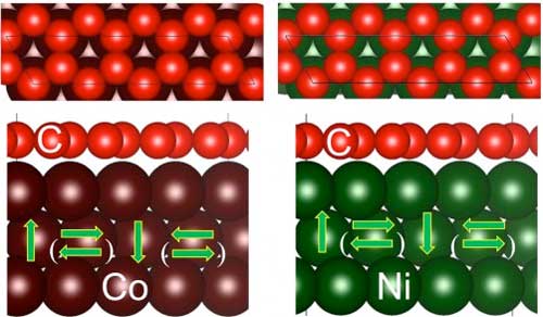
materials composed of a layer of graphene (top) with cobalt (bottom left) and with nickel (bottom right)
A view from above (top) and the side (bottom) of materials composed of a layer of graphene (top) with cobalt (bottom left) and with nickel (bottom right). The spin configurations are represented by arrows. (© Nature Materials)
“Calculations by other team members show that if you take different magnetic materials and graphene and build a multilayer stack of many repeating structures, then this phenomenon and effect could possibly be very powerfully amplified,” Schmid said.
To measure the layered material, scientists applied spin-polarized low-energy electron microscopy (SPLEEM) using an instrument at the Molecular Foundry’s National Center for Electron Microscopy. It is one of just a handful of specialized devices around the world that allow scientists to combine different images to essentially map the orientations of a sample’s 3-D magnetization profile (or vector), revealing a its „spin textures.”
The research team also created the samples using the same SPLEEM instrument through a precise process known as molecular beam epitaxy, and separately studied the samples using other forms of electron-beam probing techniques.
Gong Chen, a co-lead author who participated in the study as a postdoctoral researcher at the Molecular Foundry and is now an assistant project scientist in the UC Davis Physics Department, said the collaboration sprang out of a discussion with French scientists at a conference in 2016 – both groups had independently been working on similar research and realized the synergy of working together.
While the effects that researchers have now observed in the latest experiments had been discussed decades ago in previous journal articles, Chen noted that the concept of using an atomically thin material like graphene in place of heavy elements to generate those effects was a new concept.
„It has only recently become a hot topic,” Chen said. „This effect in thin films had been ignored for a long time. This type of multilayer stacking is really stable and robust.”
Using skyrmions could be revolutionary for data processing, he said, because information can potentially be stored at much higher densities than is possible with conventional technologies, and with much lower power usage.
Molecular Foundry researchers are now working to form the graphene-magnetic multilayer material on an insulator or semiconductor to bring it closer to potential applications, Schmid said.
Source: Lawrence Berkeley National Laboratory

Strălucind ca un nanoagregat(Shine bright like a nanoaggregate)

au transformat moleculele cluster-cupru-iod in nanostructuri agregate, foarte luminescente, pentru a fi utilizate in diode emiteoare de lumina (LED). Ansamblurile în stare solidă, fabricate din complexe ale grupului de cupru-iod cu compuși organici fosforici ca liganzi, sunt ușor de preparat, ieftin și pot emite lumină în mai multe culori, se arată în revista Angewandte Chemie ( „Highly Luminescent Inks: Aggregation- Emisiile induse de clustere hibride de cupru-iod ” ). Nanoagregatele pot fi utilizate ca cerneluri luminiscente pentru picturi invizibile și acoperiri colorate pentru LED-uri.Aici, cercetatorii au acoperit surse albastre cu LED-uri cu hibrizi galbeni luminescenti de cupru-iod si au observat ca emisia de LED-uri devine alba

Posted: May 25, 2018

Shine bright like a nanoaggregate

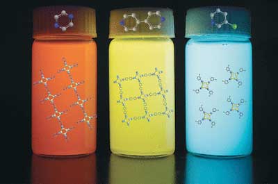
(Nanowerk News) Chinese scientists have turned copper–iodine cluster molecules into aggregated, highly luminescent nanostructures for use in light-emitting diodes (LEDs). The solid-state assemblies made of complexes of the copper–iodine cluster with phosphor–organic compounds as ligands are easily prepared, cheap, and can emit light in many colors, they report in the journal Angewandte Chemie („Highly Luminescent Inks: Aggregation-Induced Emission of Copper–Iodine Hybrid Clusters”). The nanoaggregates can be used as luminescent inks for invisible paintings and color coatings for LEDs.

Highly luminescent inks made from copper–iodine hybrid clusters with aggregation-induced emission
Shine Bright Like a Nanoaggregate – Highly luminescent inks made from copper–iodine hybrid clusters with aggregation-induced emission. (© Wiley-VCH)
Luminescence is light emission triggered by some form of energy, which can be chemical, electrical, or radiation. For a long time, scientists thought that aggregation would be detrimental to luminescence. But in some substances, aggregation can be beneficial, researchers reported for the first time in 2001 when they observed that conformational changes turned a weak luminophore into a strong emitter. Since then, research on the so-called aggregation-induced emission (AIE) compounds has grown fast. One of the reasons: in real-world applications such as luminescent coatings and inks, the pigments usually adopt an aggregated state.
The team led by Hong-Bin Yao at the University of Science and Technology of China in Hefei, China, explores the preparation routes to AIE compounds, with the goal to prepare inks on a larger scale and without a big budget. A stable cluster of copper and iodine grabbed their attention. In combination with common phosphine ligands, this cluster was known to exhibit strong luminescence in its aggregated state, the typical AIE phenomenon. But a reliable way to get to that state, let alone applications, were not reported.
To prepare the AIE emitter, the starting compound must be present as a single, soluble molecule, then it is assembled and turned into something nanoparticular and non-soluble. The authors tackled the problem by employing an emulsifying–demulsifying process. By shaking the non-emitting complex dissolved in an organic solvent with a surfactant, they managed to confine the copper–iodine hybrid clusters in small droplets to obtain AIE-active nanoaggregates in a simple but effective way.
The method has another advantage: when swapping the ligands of the complex, the colors changed. The scientists replaced the phosphor ligand with a set of nitrogen-containing ligands and obtained a beautiful array of luminescent inks in colors ranging from orange to blue. With which they clearly enjoyed painting: Using their aqueous inks luminescing in orange, yellow, and sky-blue, they transformed a black-and-white sketch of an underwater world into an atmospheric exquisite aquarelle visible only under UV light.
Not only inks for paintings, but also color coatings for LED lamps were prepared. Normally, white LED light is difficult to achieve. Here, the researchers coated blue LED sources with yellow luminescent copper–iodine hybrids and observed the LED emission turning white. However, some adjustments still need to be made to increase the efficiency, the authors admitted.
Source: Wiley

Element rar pentru a oferi un material mai bun pentru electronica de mare viteză(Rare element to provide better material for high-speed electronics)

au descoperit un nou material bidimensional, derivat din telurul elementului rar, pentru a face tranzistoare care transporta un curent mai bun pe tot parcursul unui cip de calculator., materialul ar putea fi utilizat în alte aplicații, în afara tranzistorilor cu cipuri de calculator, cum ar fi dispozitivele imprimate flexibile care convertesc vibrațiile mecanice sau căldura electrică.

Posted: May 24, 2018

Rare element to provide better material for high-speed electronics

(Nanowerk News) Purdue researchers have discovered a new two-dimensional material, derived from the rare element tellurium, to make transistors that carry a current better throughout a computer chip.

The discovery adds to a list of extremely thin, two-dimensional materials that engineers have tried to use for improving the operation speed of a chip’s transistors, which then allows information to be processed faster in electronic devices, such as phones and computers, and defense technologies like infrared sensors.
Other two-dimensional materials, such as graphene, black phosphorus and silicene, have lacked either stability at room temperature or the feasible production approaches required to nanomanufacture effective transistors for higher speed devices.
“All transistors need to send a large current, which translates to high-speed electronics,” said Peide Ye, Purdue’s Richard J. and Mary Jo Schwartz Professor of Electrical and Computer Engineering. “One-dimensional wires that currently make up transistors have very small cross sections. But a two-dimensional material, acting like a sheet, can send a current over a wider surface area.”
Tellurene, a two-dimensional film researchers found in the element tellurium, achieves a stable, sheet-like transistor structure with faster-moving “carriers” – meaning electrons and the holes they leave in their place. Despite tellurium’s rarity, the pros of tellurene would make transistors made from two-dimensional materials easier to produce on a larger scale. The researchers detail their findings in Nature Electronics („Field-effect transistors made from solution-grown two-dimensional tellurene”).
“Even though tellurium is not abundant on the Earth’s crust, we only need a little bit to be synthesized through a solution method. And within the same batch, we have a very high production yield of two-dimensional tellurene materials,” said Wenzhuo Wu, assistant professor in Purdue’s School of Industrial Engineering. “You simply scale up the container that holds the solution, so productivity is high.”
computer chip transistors made with two-dimensional tellurene
A small quantity of two-dimensional tellurene, derived from the rare element tellurium, can make computer chip transistors both more scalable and efficient. (Image: Vincent Walter, Purdue University)
Since electronics are typically in use at room temperature, naturally stable tellurene transistors at this temperature are more practical and cost-effective than other two-dimensional materials that have required a vacuum chamber or low operation temperature to achieve similar stability and performance.
The larger crystal flakes of tellurene also mean less barriers between flakes to electron movement – an issue with the more numerous, smaller flakes of other two-dimensional materials.
“High carrier mobility at room temperature means more practical applications,” Ye said. Faster-moving electrons and holes then lead to higher currents across a chip.
The researchers anticipate that because tellurene can grow on its own without the help of any other substance, the material could possibly find use in other applications beyond computer chip transistors, such as flexible printed devices that convert mechanical vibrations or heat to electricity.
“Tellurene is a multifunctional material, and Purdue is the birthplace for this new material,” Wu said. “In our opinion, this is much closer to the scalable production of two-dimensional materials with controlled properties for practical technologies.”
Source: By Kayla Wiles, Purdue University

Filme funcționale realizate din minerale și coloranți din argilă ecologică(Functional films made of environmentally friendly clay minerals and dyes)

au creat un film hibrid transparent care imbina mineralele naturale de argila si coloranti intr-un material care schimba culoarea ca raspuns la umiditatea mediului. Schimbarea culorii nu implică ruperea legăturilor chimice; echipa a descoperit un mecanism nou care face procesul ușor de reversibil, pentru o funcționalitate de lungă durată folosind materiale ecologice. Aplicațiile includ senzori de mediu și amplificarea luminii de ultimă oră în afișaje.

Posted: May 17, 2018

Functional films made of environmentally friendly clay minerals and dyes

(Nanowerk News) Researchers from Tokyo Metropolitan University and Shimane University have created a transparent hybrid film that combines natural clay minerals and dyes into a material that changes color in response to environmental humidity. The color change does not involve breaking chemical bonds; the team uncovered a novel mechanism that makes the process easily reversible, for long-lasting functionality using environmentally friendly materials. Applications include environmental sensors, and state-of-the-art light amplification in displays.

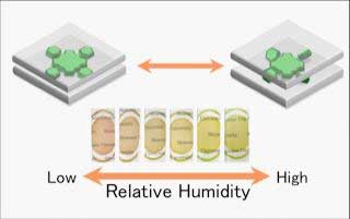
Transparent hybrid film composed of environmentally friendly clay minerals and dyes, that changes color with humidity
Transparent hybrid film composed of environmentally friendly clay minerals and dyes, that changes color with humidity via a novel mechanism. (Image: Shinsuke Takagi)
Combining dyes with a wide range of natural minerals like clathrates (clays) and zeolites (porous rock) is a widely applied, promising strategy for creating hybrid materials that can interact with light, or „chromic” materials.
The physical structure of these materials plays a key role; tiny, nanometer-sized cavities play host to light-sensitive molecules which behave differently from when they are free in solution, with potential applications to light emitting devices, light harvesting (like in solar cells) and novel sensors.
A team led by Prof Takuya Fujimura from the Department of Physics and Materials Science, Shimane University, and Prof Shinsuke Takagi from the Department of Applied Chemistry, Tokyo Metropolitan University, have created a transparent film made of an environmentally-friendly clay mineral and a dye, magnesium porphyrin, that changes color in response to humidity (Langmuir, „Optical Humidity Sensing Using Transparent Hybrid Film Composed of Cationic Magnesium Porphyrin and Clay Mineral”).
What makes this film special is the mechanism by which it achieves such a striking change. Clays have a layered structure, with nanometer-scale thin spaces in between. The team made a technical breakthrough in getting the dye into these gaps without forming aggregates, to ensure an effective response. The clay layers change their spacing in response to humidity; the confinement of the dye changes.
More specifically, the electrons surrounding the dye molecule, particularly those involved in how it interacts with light, are made to line up with certain chemical groups in the clay, dramatically changing its color. Note that no chemical bonds are broken or made. This makes the film more compatible with repeated switching, with less degradation of the material.
The film is not just more durable. Both the clay and dye could be naturally derived materials. That means lower cost, improved safety and enhanced compatibility with the environment. The team hopes to apply the film and new mechanism to sensors and amplification in light emitting devices.
Source: Tokyo Metropolitan University

Dispozitivul nou ar putea crește durata de viață a bateriei electronice de o sută de ori(New device could increase battery life of electronics by a hundred-fold)

a dezvoltat un material de dispozitiv care poate aborda ambele probleme. Echipa a solicitat un brevet pentru un material magnetic care utilizează o structură unică – o latură „fagure de miere” care prezintă proprietăți electronice distincte.

Posted: May 16, 2018

New device could increase battery life of electronics by a hundred-fold

(Nanowerk News) Among the chief complaints for smartphone, laptop and other battery-operated electronics users is that the battery life is too short and–in some cases–that the devices generate heat. Now, a group of physicists led by Deepak K. Singh, associate professor of physics and astronomy at the University of Missouri, has developed a device material that can address both issues. The team has applied for a patent for a magnetic material that employs a unique structure–a „honeycomb” lattice that exhibits distinctive electronic properties.

„Semiconductor diodes and amplifiers, which often are made of silicon or germanium, are key elements in modern electronic devices,” said Singh, who also serves as the principal investigator of the Magnetism and Superconductivity Research Laboratory at MU. „A diode normally conducts current and voltage through the device along only one biasing direction, but when the voltage is reversed, the current stops. This switching process costs significant energy due to dissipation, or the depletion of the power source, thus affecting battery life. By substituting the semiconductor with a magnetic system, we believed we could create an energetically effective device that consumes much less power with enhanced functionalities.”
Singh’s team developed a two-dimensional, nanostructured material created by depositing a magnetic alloy, or permalloy, on the honeycomb structured template of a silicon surface. The new material conducts unidirectional current, or currents that only flow one way. The material also has significantly less dissipative power compared to a semiconducting diode, which is normally included in electronic devices.
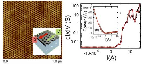
honeycomb structure pattern behind a magnetic device
The left shows the atomic force micrograph, exhibiting honeycomb structure pattern behind a magnetic device. Inset shows the schematic of current flow direction. On the right: electrical data reveals diode-type behavior of current flowing in one direction. Inset shows that the dissipative power is of the order of nano-watt in the current flowing direction, which is at least three orders of magnitude smaller than the semiconductor diode. (Image: Deepak Singh)
The magnetic diode paves the way for new magnetic transistors and amplifiers that dissipate very little power, thus increasing the efficiency of the power source. This could mean that designers could increase the life of batteries by more than a hundred-fold. Less dissipative power in computer processors could also reduce the heat generated in laptop or desktop CPUs.
„Although more works need to be done to develop the end product, the device could mean that a normal 5-hour charge could increase to more than a 500-hour charge,” Singh said. „The device could also act as an ‘on/off switch’ for other periphery components such as closed-circuit cameras or radio frequency attenuators, which reduces power flowing through a device. We have applied for a U.S. patent and have begun the process of incorporating a spin-off company to help us take the device to market.”
The proposed startup company associated with this research, highlights the university’s impact on the state’s economic development efforts, including commercialization of research conducted at Mizzou, workforce development and job growth, quality of life improvements for residents, and attracting corporations and businesses to the state. Companies commercializing MU technologies have secured hundreds of millions of dollars in investments and grants to advance their commercialization efforts. In 2017, the Office of Technology Management and Industry Relations reported that 31 U.S. patents were issued to members of the MU community.
The studies, „Magnetic Diode Behavior at Room Temperature in 2D Honeycombs” and „Spin Solid versus Magnetic Charge Ordered State in Artificial Honeycomb Lattice of Connected Elements,” were published in Advanced Electronic Materials and Advanced Science, respectively.
Source: University of Missouri-Columbia
Subscribe to a free copy of one of our daily
Nanowerk Newsletter Email Digests
with a compilation of all of the day’s news.