Efectuarea de supraconductoare noi stratificate folosind aliaje de entropie ridicată(Making new layered superconductors using high entropy alloys)

au creat noi superconductori din straturi de sulfură de bismut (BiS2) și o fluorfluorură de aliaj de pământuri rare de entropie, conținând cinci elemente diferite de pământuri rare în același sit cristalografic. Noul material păstrează proprietățile supraconductoare într-o gamă mai largă de parametri de zăcământ decât materiale fără stări de aliaj cu entropie ridicată.

Posted: May 04, 2018

Making new layered superconductors using high entropy alloys

(Nanowerk News) Researchers from Tokyo Metropolitan University have created new superconductors made of layers of bismuth sulfide (BiS2) and a high entropy rare earth alloy oxyfluoride, containing five different rare earth (RE) elements at the same crystallographic site. The new material retains superconducting properties over a wider range of lattice parameters than materials without high-entropy-alloy states.

Their work promises an exciting new strategy for designing new layered superconductors, a potentially key development in the search for high-temperature superconductors (Applied Physics Express, „Superconductivity in REO0.5F0.5BiS2 with high-entropy-alloy-type blocking layers”).
This is a schematic image of the crystal structure of high-entropy-alloy-type REO0.5F0.5BiS2
This is a schematic image of the crystal structure of high-entropy-alloy-type REO0.5F0.5BiS2. (Image: Yoshikazu Mizuguchi)
Superconductors are key to a range of exciting potential applications. For example, zero resistivity promises loss-free power transmission and powerful electromagnets. The challenge has been to discover a material that retains this property at higher temperatures, closer to ambient temperatures. Despite focused work and a number of breakthroughs in recent years, the hunt is still on for effective strategies to create new superconducting materials.
One strategy is the use of layered materials with a molecular structure consisting of alternating superconducting layers and „blocking layers” acting as insulating spacers. A team led by Associate Professor Yoshikazu Mizuguchi from the Department of Physics, Tokyo Metropolitan University, has uncovered an important aspect of designing the insulating layer. They were able to combine five different rare earth (RE) elements, lanthanum, cerium, praseodymium, neodymium, and samarium, and create a „high entropy alloy” in the blocking layer.
High entropy alloys have attracted considerable attention in recent years for their toughness, resistance to fatigue and ductility, amongst many other notable physical properties.
The team’s new materials, with different proportions of REs (10-30%), exhibited enhanced superconducting properties; in particular, materials with the same period in their molecular structure exhibited a superconducting transition at higher temperatures when the blocking layer contained a high entropy alloy. They believe that the high entropy alloy helps to stabilize the crystal structure of the superconducting layer.
The work’s impact is not limited to the new materials they present. Given the existence of a large number of superconducting layers which are compatible with RE oxides, this innovation opens the way for a broad new strategy for engineering new, revolutionary superconducting materials.
Source: Tokyo Metropolitan University

Inginerii dezvoltă o metodă nouă de rezolvare a texturii de spin a stărilor topologice de suprafață utilizând măsurători de transport(Engineers develop novel method for resolving spin texture of topological surface states using transport measurements)

Efectul de magneto-rezistență este tendința unui material de a schimba valoarea rezistenței sale electrice într-un câmp magnetic aplicat extern. Acesta a fost folosit pe scară largă pentru aplicații în senzori și capete de citire pe hard disk. Până în prezent, nu a fost stabilită nici o legătură între magnitorezistențele existente și textura spinării materialelor spin-polarizate. Cercetătorii de la Universitatea Națională din Singapore (NUS) au făcut recent un progres în acest domeniu, dezvăluind o strânsă legătură între textura de spin a stărilor de suprafață topologică (TSS) și un nou tip de rezistență la magneto.Rezultatele noastre pot fi aplicate la familii extinse de materiale foarte spin-polarizate, cum ar fi sistemele Rashba / Dresselhaus, precum si dichalcogenidele cu tranzitie bidimensionala cu stari spin-polarizate. De asemenea, oferă o nouă cale de detectare a texturii 3D a acestor materiale printr-o simplă măsurătoare de transport. „

Posted: Apr 26, 2018

Engineers develop novel method for resolving spin texture of topological surface states using transport measurements

(Nanowerk News) The magneto-resistance effect is the tendency of a material to change the value of its electrical resistance in an externally-applied magnetic field. It has been widely utilised for applications in sensors and hard disk reading heads. So far, no link has been established between the existing magneto-resistances and spin texture of spin-polarised materials. Researchers from the National University of Singapore (NUS) have recently made a breakthrough in this field, revealing a close relation between the spin texture of topological surface states (TSS) and a new kind of magneto-resistance.

This fundamental advancement is achieved in collaboration with researchers from the University of Missouri, United States. The research team observed for the first time a novel magneto-resistance in three-dimensional (3D) topological insulators (TIs), which scales linearly with both the applied electric and magnetic fields, and shows a close link to the in-plane and out-of-plane spin textures of TSS. The team’s finding could help in addressing the issue of spin current source selection often faced in the development of spintronic devices.
The research team, led by Associate Professor Yang Hyunsoo from the Department of Electrical and Computer Engineering at the NUS Faculty of Engineering, published their findings in the journal Nature Physics („Bilinear magnetoelectric resistance as a probe of three-dimensional spin texture in topological surface states”).
Bilinear magnetoelectric resistance as a probe of three-dimensional spin texture in topological surface states
(a) Schematic diagram illustrating the Dirac cone of a topological insulator. (b) Spin-momentum locked surface state with hexagonal warping. (c,d) Hall bar device of topological insulator Bi2Se3for harmonic resistance measurements. (e) Second harmonic resistance signal for the three scans of magnetic fields in xy, zy, and zx planes. (Image: NUS) (click on image to enlarge)

New magneto-resistance found in 3D TI

The discovery of 3D TIs has generated great interest among international researchers to understand the physical properties of this new state of matter, and exploring its applications in optoelectronics and spintronics. So far, the magneto-resistances found in 3D TIs is current-independent, reflecting a linear response of the electron transport to an applied electric field. At the same time, a transport obstacle exists in detecting the surface properties, due to the significant bulk contribution, which overwhelms the surface responses.
“In this work, we observed the second order nonlinear magneto-resistance in a prototypical 3D TI Bi2Se3 films, and showed that it is sensitive to TSS. In contrast with conventional magneto-resistances, this new magneto-resistance shows a linear dependence on both the applied electric and magnetic fields,” said Dr He Pan, who is the first author of the study and a Research Fellow at the Department.
Assoc Prof Yang added, “Theoretical calculations by our collaborators from the University of Missouri revealed that the bilinear magneto-electric resistance originates from the spin-momentum locked TSS with hexagonal warping. From the perspective of the microscopic origin, it is a fundamentally new process regarding the conversion of a nonlinear spin current into a charge current under the external magnetic field.”

Novel technique to probe 3D spin texture

Probing the surface spin texture is of critical importance for the development of TI-based spintronic devices. However, the approach performed to date is highly restricted to sophisticated tools such as photoemission spectroscopy.
The novel magneto-electric resistance observed by the research team provides a new route to detect the 3D spin texture in TSS by a simple electric transport measurement without involving any additional ferromagnetic layers. The team’s study also revealed the hexagonal warping effect in TSS, which could previously only be determined by photoemission spectroscopy.
Commenting on the significance of the breakthrough, Dr He Pan said, “Our results can be applied to extended families of highly spin-polarised materials, like Rashba/Dresselhaus systems as well as two-dimensional transition metal dichalcogenides with spin-polarised states. It also provides a new route to detect the 3D spin texture of these materials by a simple transport measurement.”

Next steps

Moving forward, Assoc Prof Yang and his team are conducting experiments to increase the magnitude of the novel magneto-resistance by refining the TI materials and film thickness. They are also planning to incorporate and test the technology in different materials. The team hopes to work with industry partners to explore various applications with the novel magneto-resistance.
Source: National University of Singapore

Grafenul modifică proprietățile elastice în funcție de forța aplicată(Graphene changes elastic properties depending on applied force)

vor prezenta proprietăți speciale” , Note Kachorovskii.
Faptul că grafenul se poate întinde în mod normal sau anormal în funcție de forța aplicată în perspectivă va ajuta, de exemplu, la crearea de senzori de sunet hipersensibili.
„Undele sonore întind membrana grafenului și, în funcție de gradul de întindere, grafenul modifică semnificativ rezistența electrică.” Calculele arată că sensibilitatea unui astfel de detector poate fi gigantică, în plus, viteza sonoră este semnificativ mai mare decât în ​​materialele „normale”. Valoarea altor constante elastice, de exemplu modulul lui Young, ramane acelasi. De aceea, atunci cand grafenul devine intins la starea de auxetic, sunetul se raspandeste foarte repede, ceea ce ne permite sa cream senzori ultra-rapizi care pot detecta schimbare foarte rapidă a oscilațiilor

Posted: Apr 19, 2018

Graphene changes elastic properties depending on applied force

(Nanowerk News) A group of scientists, including specialists from Landau Institute for Theoretical Physics (ITF), described a universal characteristic, in which many unique graphene properties are „hidden”. It turned out that abnormal graphene behavior can be fully characterised by Poisson ratio, which determines material capability to shrink or extend in transverse dimension. Moreover,scientists found key factors that can influence this characteristic. The results are published in Physical Review B („Stress-controlled Poisson ratio of a crystalline membrane: Application to graphene”).

Folded elements of auxetic materials straighten out, increasing its transverse dimension under stretching
a) Folded elements of auxetic materials straighten out, increasing its transverse dimension under stretching. b) Products made of any materials, folded according to the rules of the miura-ori: a folding system, which makes it possible to straighten the construction in one movement, also possess auxetic properties. c) Sneakers sole made up of overlapping triangles behaves like an auxetic under pressure. (Image: Article authors)
Graphene is a two-dimensional sheet consisting of one layer of carbon atoms. Due to its unusual properties, today graphene is considered one of the most promising materials for new non-silicon elastic electronics. One of the most interesting things about graphene is the relation between its unique elastic and electrical properties. For instance, graphene shows extremely high mobility of electric charges, which can change drastically under elastic stress. Physicists tried to find a universal physical characteristic fully reflecting this unusual behaviour. This would make it possible to use graphene more effectively, as well as create new materials with required exotic properties. However, until recently researchers could not find any such parameter.
The key to understanding this question lied in the unusual behavior of graphene under stretching. Most common materials shrink in transverse direction while stretching: a rubber band is a typical example. However, about a hundred years ago, the German physicist Voldemar Voight discovered that pyrite crystals, on the contrary, extend under stretching. Such materials were called auxetics, and in the late 1970s scientists obtained first artificial auxetic. The secret of such materials comes from their unusual geometry. Although in a relaxed state auxetic structural elements are folded, when stretching is applied they unfold and grow in size.
Auxetics have a number of unusual features that will help improve existing technologies and create new ones. „Conventional materials expand when heated and this impairs their original properties through various mechanical stresses and disturbances. Auxetics can, on the contrary, shrink. So there is an idea to create combined materials with zero expansion ratio using auxetics. As the temperature rises, the conventional compound of such materials will tend to expand, but auxetic compound will compensate for this,” comments Valentin Kachorovskii, a leading researcher at The Ioffe Institute and ITF.
The feature determining material capability to shrink or extend in transverse dimension under tension is called the Poisson ratio. In auxetics it is negative, in ordinary materials – positive. „Scientists were long interested in graphene Poisson ratio,” says Kachorovskii. „For a long time we thought that it was equal to the universal negative value -?. However, a number of recent numerical calculations showed that graphene Poisson ratio could be both positive and negative. At first glance, results of various calculations contradict each other completely.”
Direct experimental verification of this parameter is difficult. Graphene is hard to obtain in isolation: it is usually „grown” on various substrates, and their characteristics mask the true value of graphene Poisson ratio. What is more, samples of isolated graphene are so small that it is practically impossible to attach brackets for controlled stretching. At the same time, researchers and engineers who develop new carbon-based technologies need to know exactly whether graphene is auxetic or not.
Authors of the new work managed to „reconcile” contradictory results of previous calculations and find parameters that exactly determine the Poisson ratio of graphene. Physicists found out that it is a variable value depending on tensile force applied. „With a very large force, graphene behaves like a normal material, demonstrating positive Poisson ratio. However, when the applied force decreases, we find ourselves in an area where graphene exhibits typically auxetic properties,” notes Kachorovskii.
Scientists explained this unusual link between Poisson ratio and stretching. On popular images graphene is shown as a two-dimensional sheet of carbon atoms, usually flat. However, in reality so-called bending waves run along this „sheet”. They tend to turn graphene from a flat state into a crumpled state. „This is called a crumpling transition,” Kachorovskii explains.
„For a long time the theory of membranes predicted that due to this phenomenon two-dimensional crystals such as graphene could not exist in principle. They would always strive to shrink into a ball. As we see, this assumption was a mistake since along the surface of graphene ordinary compression-extension waves run along with bending ones. Nonlinear interaction between two wave types does not allow the membrane to shrink into a ball. Even though, the dimension of such crystals does not actually equal to two. Due to crumpling transition, it is in an intermediate state between two and three dimensions.”
Membrane striving to curl due to ordinary compression-extension waves competes with the effect of smoothing transverse waves due to an external applied force. This results in a changing sign of Poisson ratio. In other words, if the external force is high, the abnormal auxetic properties are suppressed and Poisson ratio is positive. As the scientists showed, the unusual properties of graphene are based on that slightly crumpled resting state.
„In folds of transverse bending waves additional energy is stored, which accounts for graphene abnormal elasticity and other unusual properties. For example, when heated graphene begins to shrink in the longitudinal direction, since the entire extension goes to transverse folds,” continues Kachorovskii. „And universal characteristic which determines exactly graphene behavior is Poisson ratio. With its help, you can describe and predict a large number of properties of graphene and other materials.”
What is more, current work contains explanation why previous studies of the Poisson ratio of graphene had contradictory results. „We derived an analytically complete system of equations for the elastic balance of graphene sheet. It turns out that there are two modes of behavior for graphene membrane. In the usual one, all the properties of graphene are determined by standard formulas and Poisson ratio is positive. At the same time, for samples larger than so-called Ginzburg length, an abnormal elasticity regime is realized, leading to negative Poisson ratio”, adds Kachorovskii. For graphene, Ginzburg’s length ranges from 40 to 70 angstroms. The size of samples used in practice is certainly greater, therefore it is possible to see the most unusual auxetic behavior.
The explanation of this phenomenon is also connected with waves of different types, which interact with each other in a very complicated manner. „Ginzburg length characterizes the scale at which these interactions can no longer be neglected as they begin to abnormally shift the material. For example, such large-scale interaction does not allow two-dimensional crystals to shrink into a ball”, explains Kachorovskii. Different substances have different Ginzburg lengths and knowing them is extremely important for the development of new materials.
„Often people create new materials without calculating Ginzburg length and then they try to find something unusual in their properties. But our work shows that if Ginzburg length is as large as 1 kilometer, for example, regular sized samples will not show any special properties”, Kachorovskii notes.
The fact that graphene can stretch normally or abnormally depending on the applied force in perspective will help create hypersensitive sound sensors, for example.
„Sound waves stretch graphene membrane, and depending on the degree of stretching graphene noticeably changes the electrical resistance. Calculations show that sensitivity of such detector can be gigantic. In addition, in auxetics the sound velocity is noticeably higher than in „normal” materials. The value of other elastic constants, for example, the Young’s modulus remains the same. Therefore, when graphene becomes stretched to the state of auxetic, the sound in it spreads very quickly. This allows us to create ultra-fast sensors which can detect a very rapid change of oscillations”, summarizes Kachorovskii.
Source: AKSON Russian Science Communication Association

Nanotehnologia purtătoare de autoturisme cu încărcare automată(Nanotechnology wearable self-charging power units)

Cercetătorii au dezvoltat un fotodetector auto-acționat prin cuplarea polimerului polimedil-siloxanic pe bază de silicon (PDMS) ca un TENG cu un material numit perovskit de halogenură organometalică¹. Materialul pe bază de halogenură de plumb prezintă proprietăți optoelectronice care sunt de dorit în celulele solare și diodele emițătoare de lumină.Dispozitivul auto-alimentat a demonstrat o reacție excelentă la lumina incidentă, în special când este expusă la lumină de intensitate redusă”, spune Mark Leung, autorul principal al studiului fotodetector. Datorită componentelor polimerice flexibile și transparente, și-a păstrat performanțele după ce a fost îndoit de 1.000 de ori și indiferent de orientarea luminii incidentate

Posted: Apr 12, 2018

Nanotechnology wearable self-charging power units

(Nanowerk News) Autonomy is a much-anticipated feature of next-generation microsystems, such as remote sensors, wearable electronic gadgets, implantable biosensors and nanorobots. KAUST researchers led by Husam Alshareef, Jr-Hau He and Khaled Salama have developed small standalone devices by integrating maintenance-free power units that produce and use their own fuel instead of relying on an external power source (Nano Energy, „MXene electrochemical microsupercapacitor integrated with triboelectric nanogenerator as a wearable self-charging power unit” and Advanced Materials, „A self-powered and flexible organometallic halide perovskite photodetector with very high detectivity”).

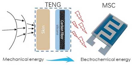
wearable power bracelet can capture and transform energy from human motion into electricity and store it in MXene supercapacitors to drive different sensors
The wearable power bracelet can capture and transform energy from human motion into electricity and store it in MXene supercapacitors to drive different sensors. (Image: KAUST)
Triboelectric nanogenerators (TENGs) capture mechanical energy from their surroundings, such as vibrations and random motion produced by humans, and convert it into electricity. In these tiny generators, frictional contact between materials of different polarity creates oppositely charged surfaces. Repeated friction causes electrons to hop between these surfaces, resulting in electric voltage.
„We exploited this triboelectric effect to harvest energy from simple movements, such as hand clapping, finger tapping and routine hand motion, to drive different types of sensors,” says Alshareef.
The researchers have developed a self-powered photodetector by coupling the silicone-based polymer polydimethylsiloxane (PDMS) as a TENG with a material called organometallic halide perovskite¹. The lead-halide-based material features optoelectronic properties that are desirable in solar cells and light-emitting diodes.
To streamline their design and eliminate the need for a motion actuator, He’s team fabricated the photodetector using two multilayered polymer-based sheets separated by a small gap. One sheet comprised the perovskite ultrathin film while the other contained a PDMS layer. The gap allowed the team to harness the triboelectric effect when the device was activated by finger tapping.
„The self-powered device showed excellent responsiveness to incident light, especially when exposed to light of low intensity”, says Mark Leung, the lead author of the photodetector study. Because of its flexible and transparent polymer components, it also retained its performance after being bent 1,000 times and regardless of the orientation of the incident light.
Pushing the boundaries further, the researchers engineered a wearable self-powered bracelet that can store the converted mechanical energy by combining a carbon-fiber-embedded silicone nanogenerator with MXene microsupercapacitors².
They incorporated nanogenerator and miniaturized electrochemical capacitors into a single monolithic device encased in silicone rubber. The leak-proof and stretchable shell provided a flexible and soft bracelet that fully conformed to the body. Fluctuations in the skin-silicone separation altered the charge balance between electrodes, causing the electrons to flow back and forth across the TENG and the microsupercapacitor to charge up.
In addition to exhibiting longer cycle life and short charging time, MXene microsupercapacitors can accumulate more energy in a given area than thin-film and micro-batteries, offering faster and more effective small-scale energy storage units for TENG-generated electricity. When active, the bracelet can use the stored energy to operate various electronic devices, such as watches and thermometers.
„Our ultimate goal is to develop a self-powered sensor platform for personalized health monitoring,” says Ph.D. student Qiu Jiang, the lead author of the self-charging band project. The team is now planning to introduce sensors into the system to detect biomarkers in human sweat.
Source: KAUST

Știința tubulară îmbunătățește celulele solare polimerice(Tubular science improves polymer solar cells)

Centrul pentru Materiale Nanoscale și echipa de la Universitatea Stony Brook au demonstrat că adăugarea unei componente treilea polimer la amestecul binar de materiale organice cu celule solare duce la o nanostructură coloană autostopică asamblată. Acest lucru a îmbunătățit mobilitatea încărcării și performanța fotovoltaică în dispozitivele cu grosimi de strat mai mari de 300 nanometri – mai mult de trei ori mai groase decât cele tipice.

Posted: Apr 10, 2018

Tubular science improves polymer solar cells

(Nanowerk News) A popular polymer-based solar cell could produce more energy if the electronic charges can move efficiently through the cell’s components. A novel three-component mixture allows conductive solar cell materials to self-align into columns (Nanoscale, „A new strategy to engineer polymer bulk heterojunction solar cells with thick active layers via self-assembly of tertiary columnar phase”).

The alignment improves the efficiency. This, in turn, allows the solar cells to be fabricated more than three times thicker without degrading the high performance. The greater depth makes the process more compatible with conventional industrial coating processes.
Illustration of a three-component blend polymer-based solar cell
Illustration of a three-component blend polymer-based solar cell: (1) polymer plates (pink), (2) fullerene (a.k.a. buckyballs, grey spheres) active components, and (3) a columnar polymer (dark grey columns) that promotes self-assembly of efficient, columnar charge collection pathways (green arrows). (Image: Center for Functional Nanomaterials at Brookhaven National Laboratory)
Reliable manufacturing. High performance. The internal architectures formed by this new blend of three components has potential to make these materials more amenable to reliable manufacturing. The devices can be made at greater thicknesses. These depths are better suited for conventional industrial coating processes but still allow the cell to maintain its high performance.
Low-cost, large-area scalability by solution processing is an important advantage of organic polymer solar cells. Typical organic solar cells, however, require active layer thicknesses of less than 100 nanometers (about 0.000004 inches) for optimal performance, due to the limitations of polymer semiconductor charge carrier mobility. This presents a significant challenge for solution-based manufacturing—large-area coating technologies (for example, roll-to-roll or slot-die coatings) are unable to provide reliable films at such thin dimensions.
The Center for Nanoscale Materials and Stony Brook University team demonstrated that adding a third polymer component to the binary blend of organic solar cell materials leads to a self-assembled columnar nanostructure. This enhanced the charge mobility and photovoltaic performance in devices with layer thicknesses of more than 300 nanometers—more than three times thicker than typical.
Detailed experimental studies and simulations reveal that interfacial tension between the polymeric components is crucial for obtaining the self-assembled columnar nanoarchitecture that provides efficient charge extraction pathways.
Practically, this ternary blend organic solar cell architecture has potential to enable reliable large-area manufacturing because the devices can be made thicker for conventional industrial coating processes.
Source: U.S. Department of Energy, Office of Science

Lumina „relaxează” cristalul pentru a crește eficiența celulelor solare(Light ‘relaxes’ crystal to boost solar cell efficiency)

a constatat ca este cazul unui compus perovskitat ca un material eficient pentru a colecta lumina soarelui si a-l transforma in energie.Sa descoperit o iluminare constantă pentru a relaxa zăbrelele unui material asemănător perovskitei, făcând-o mai eficientă în colectarea luminii solare și transformarea acesteia în energie. Materialul stabil a fost testat pentru utilizarea celulelor solare de către oamenii de știință de la Universitatea Rice și Laboratorul Național Los Alamos.

Posted: Apr 05, 2018

Light ‘relaxes’ crystal to boost solar cell efficiency

(Nanowerk News) Some materials are like people. Let them relax in the sun for a little while and they perform a lot better.

A collaboration led by Rice University and Los Alamos National Laboratory found that to be the case with a perovskite compound touted as an efficient material to collect sunlight and convert it into energy (Science, „Light-induced lattice expansion leads to high-efficiency perovskite solar cells”).
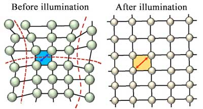
The researchers led by Aditya Mohite, a staff scientist at Los Alamos who will soon become a professor at Rice; Wanyi Nie, also a staff scientist at Los Alamos, and lead author and Rice graduate student Hsinhan (Dave) Tsai discovered that constant illumination relaxes strain in perovskite’s crystal lattice, allowing it to uniformly expand in all directions.
Constant illumination was found to relax the lattice of a perovskite-like material
Constant illumination was found to relax the lattice of a perovskite-like material, making it more efficient at collecting sunlight and converting it to energy. The stable material was tested for solar cell use by scientists at Rice University and Los Alamos National Laboratory. (Credit: Light to Energy Team/Los Alamos National Laboratory)
Expansion aligns the material’s crystal planes and cures defects in the bulk. That in turn reduces energetic barriers at the contacts, making it easier for electrons to move through the system and deliver energy to devices.
This not only improves the power conversion efficiency of the solar cell, but also does not compromise its photostability, with negligible degradation over more than 1,500 hours of operation under continuous one-sun illumination of 100 milliwatts per cubic centimeter.
The research, which appears this week in Science, represents a significant step toward stable perovskite-based solar cells for next generation solar-to-electricity and solar-to-fuel technologies, according to the researchers.
“Hybrid perovskite crystal structures have a general formula of AMX3, where A is a cation, M is a divalent metal and X is a halide,” Mohite said. “It’s a polar semiconductor with a direct band gap similar to that of gallium arsenide.
“This endows perovskites with an absorption coefficient that is nearly an order of magnitude larger than gallium arsenide (a common semiconductor in solar cells) across the entire solar spectrum,” he said. “This implies that a 300-nanometer thick film of perovskites is sufficient to absorb all the incident sunlight. By contrast, silicon is an indirect band gap material that requires 1,000 times more material to absorb the same amount of sunlight.”
Mohite said researchers have long sought efficient hybrid perovskites that are stable in sunlight and under ambient environmental conditions.
“Through this work, we demonstrated significant progress in achieving both of these objectives,” he said. “Our triple-cation-based perovskite in a cubic lattice shows excellent temperature stability at more than 100 degrees Celsius (212 degrees Fahrenheit).”
The researchers modeled and made more than 30 semiconducting, iodide-based thin films with perovskite-like structures: Crystalline cubes with atoms arranged in regular rows and columns. They measured their ability to transmit current and found that when soaked with light, the energetic barrier between the perovskite and the electrodes largely vanished as the bonds between atoms relaxed.
They were surprised to see that the barrier remained quenched for 30 minutes after the light was turned off. Because the films were kept at a constant temperature during the experiments, the researchers were also able to eliminate heat as a possible cause of the lattice expansion.
Measurements showed the “champion” hybrid perovskite device increased its power conversion efficiency from 18.5 percent to 20.5 percent. On average, all the cells had a raised efficiency above 19 percent. Mohite said perovskites used in the study were 7 percent away from the maximum possible efficiency for a single-junction solar cell.
He said the cells’ efficiency was nearly double that of all other solution-processed photovoltaic technologies and 5 percent lower than that of commercial silicon-based photovoltaics. They retained 85 percent of their peak efficiency after 800 hours of continuous operation at the maximum power point, and their current density showed no photo-induced degradation over the entire 1,500 hours.
“This work will accelerate the scientific understanding required to achieve perovskite solar cells that are stable,” Mohite said. “It also opens new directions for discovering phases and emergent behaviors that arise from the dynamical structural nature, or softness, of the perovskite lattice.”
The lead researchers indicated the study goes beyond photovoltaics as it connects, for the first time, light-triggered structural dynamics with fundamental electronic transport processes. They anticipate it will lead to technologies that exploit light, force or other external triggers to tailor the properties of perovskite-based materials.
Source: Rice University

Cerneala inteligentă adaugă noi dimensiuni imprimării 3D(Smart ink adds new dimensions to 3-D printing)

Cercetătorii de la Dartmouth College au dezvoltat o cerneală inteligentă care transformă structurile tipărite 3D în obiecte care pot schimba forma și culoarea. Inovația promite să adauge și mai multă funcționalitate imprimării 3D și ar putea deschide calea către o nouă generație de materiale tipărite

Posted: Apr 04, 2018

Smart ink adds new dimensions to 3-D printing

(Nanowerk News) Researchers at Dartmouth College have developed a smart ink that turns 3D-printed structures into objects that can change shape and color. The innovation promises to add even more functionality to 3D printing and could pave the way to a new generation of printed material.

The advancement in the area of form-changing intelligent printing – also known as 4D printing – provides a low-cost alternative to printing precision parts for uses in areas ranging from biomedicine to the energy industry.
„This technique gives life to 3D-printed objects,” said Chenfeng Ke, an assistant professor of chemistry at Dartmouth. „While many 3D-printed structures are just shapes that don’t reflect the molecular properties of the material, these inks bring functional molecules to the 3D printing world. We can now print smart objects for a variety of uses.”
Many 3D printing protocols rely on photo-curing resins and result in hard plastic objects with rigid, but random molecular architectures. The new process allows designers to retain specific molecular alignments and functions in a material and converts those structures for use in 3D printing.
By using a combination of new techniques in the pre-printing and post-printing processes, researchers were able to reduce printed objects to 1 percent of their original sizes and with 10-times the resolution. The 3D printed objects can even be animated to repeatedly expand and contract in size through the use of supramolecular pillars. With fluorescent trackers, the objects can be made to change color in response to an external stimulus such as light.
The ability to reduce the size of an object after printing while preserving functional features and increasing resolution allows inexpensive printers to print high-resolution objects that were once only possible with much more sophisticated printers.
3-D-printed object composed of hydrogel (G1) can change size after printing
An example from the research shows how a 3-D-printed object composed of hydrogel (G1) can change size after printing. While this example serves to demonstrate the result, other objects can be used as filters or storage devices. (Image: Chenfeng Ke) (click on image to enlarge)
According to the study, which was selected as a VIP paper by Angewandte Chemie („Hierarchical Co-Assembly Enhanced Direct Ink Writing”), the journal of the German Chemical Society, the smart ink can print at a rough, 300-micron resolution, but the end product would feature a much finer line width of 30 microns.
„This process can use a $1,000 printer to print what used to require a $100,000 printer,” said Ke. „This technique is scalable, widely adaptable and can dramatically reduce costs.”
To create the smart ink, researchers used a polymer-based „vehicle” that integrates intelligent molecular systems into printing gel and allows for the transformation of their functions from the nanosacle to the macroscale.
While most materials are readily hardened during the 3D printing process, the new process introduces a series of post-printing reactions which lock the active ingredients together and retain the form of the molecular structure throughout the printing process.
The result is a printed object with a molecular design that is programmed to transform itself: If you provide it with chemical fuel, it changes shape. If you shine a light on it, it can change color.
„This is something we’ve never seen before. Not only can we 3D print objects, we can tell the molecules in those objects to rearrange themselves at a level that is viewable by the naked eye after printing. This development could unleash the great potential for the development of smart materials,” Ke said.
While researchers believe the technology is still far away from intelligent 3D systems that can dynamically change their configuration, current uses for the technology could be to print precision filters and storage devices. Over time, researchers expect that the process could result in a new class of macroscale 3D printed objects that can be used to deliver medicine or produce high resolution bone replacements.
According to the research team involved in the study: „We believe this new approach will initiate the development of small molecule-based 3D printing materials and greatly accelerate the development of smart materials and devices beyond our current grasp that are capable of doing complex tasks in response to environmental stimuli.”
In the immediate term, researchers expect the smart inks to be useful to materials chemists, 3D printing engineers and others interested in bringing functional materials into 3D printing.
Source: Dartmouth College

Un nou model de metasurface arată potențialul de a controla reflexia undei acustice(A new metasurface model shows potential to control acoustic wave reflection)

Aceste metasurfe ar putea avansa în mod semnificativ tehnologiile de control al zgomotului, deoarece ar putea izola mai bine principala problemă în controlul zgomotului: frecvențe joase. „Dacă convertiți energia la frecvențe mai mari, atunci puteți să o absorbi mai ușor mai târziu”, a spus Tournat.
El citează, de asemenea, că metasurfurile subțiri pot deveni componente ale unor dispozitive mai complexe, cum ar fi diodele acustice și tranzistoarele. Aceste constatări ar putea fi aplicate și altor tipuri de valuri. În optică, metasurfurile bazate pe un concept similar „ar putea înlocui cristalele generatoare de armonice secundare (SHG) folosite pentru a dubla frecvența unui laser în transmisie”, a spus Tournat.Factorii structurali din metafore, cum ar fi aranjamentul spațial al moleculelor sale și compoziția lor, stau la baza proprietăților lor optice, elastice și acustice.

Posted: Apr 03, 2018

A new metasurface model shows potential to control acoustic wave reflection

(Nanowerk News) An international team of researchers showed how a nonlinear elastic metasurface could convert a wave’s fundamental frequency to its second harmonic. Structural factors in metasurfaces, like the spatial arrangement of its molecules and its composition, underpin its optical, elastic and acoustic properties. Developing this metasurface could help architects reduce noise from performance halls to cityscapes. These findings could also enhance cloaking technology for submarines to evade sonar detection.

Typically, when a soundwave strikes a surface, it reflects back at the same fundamental frequency with a different amplitude. Their model, reported in the Journal of Applied Physics („Manipulating acoustic wave reflection by a nonlinear elastic metasurface”), shows that when a sound wave hits this metasurface, the incident fundamental frequency does not bounce back. Instead, the metasurface converts that energy into the wave’s second harmonic resonance.
Vincent Tournat, a senior research scientist in acoustics at France’s CNRS and an author on the paper, explained that “you send a A440 pitch and after reflection, this is transformed into A880 pitch.” He expounded that this wave conversion is possible “with a thin reflecting surface … much less than the acoustic wavelength.”
Tournat reports that they are among the first acoustics groups to study nonlinear acoustic metasurfaces. Their lab focuses on nonlinear acoustics, which describes high amplitude wave interactions with nonlinear elements or media. For example, this subfield studies how a sound interacts with cracks in a solid material, or how elastic waves interact with highly deformable structures.
The team developed their new metasurface concept from past experimental work. Previously, they printed soft rubber materials like PDMS, a silicon based polymer, arranged the components in rotating square configurations, and sent soundwave pulses through the structures. When pulses propagated through PDMS structures with a particular geometry, the researchers observed a strange effect: the propagation of solitons, stable nonlinear wave pulses. As a result, the highly deformable structure appeared as an ideal platform to design a specific elastic nonlinearity.
These metasurfaces could significantly advance noise control technologies because they could better isolate the main problem in noise control: low frequencies. “If you convert the energy to higher frequencies, then you can more easily absorb it later,” Tournat said.
He also cites that thin metasurfaces could become components of more complex devices like acoustic diodes and transistors. These findings could even be applied to other types of waves. In optics, metasurfaces based on a similar concept “could replace second harmonic generation (SHG) crystals used to double the frequency of a laser in transmission,” Tournat said.
These unexpected reflections are almost like a funhouse mirror for sound. “It would be analogous to look at you in a mirror and have a reflected image shifted in the ultraviolet optical range,” Tournat said. Moving forward, the team now aims to build the metasurface and experimentally test their findings.
Source: American Institute of Physics

Cercetătorii dezvoltă filme nanoparticule pentru stocarea datelor cu densitate mare(Researchers develop nanoparticle films for high-density data storage)

Cercetătorii au creat un nanofilm care să stocheze datele holografic și să fie stabil din punct de vedere ecologic.Înregistrarea unei imagini holografice în pelicule de titan-argint implică utilizarea unui laser pentru a transforma particulele de argint în cationi de argint, care au o încărcătură pozitivă datorată electronilor extra. „Am observat că lumina UV ar putea șterge datele, deoarece a determinat transferul electronilor de la pelicula semiconductoarelor la nanoparticulele metalice, determinând aceeași transformare fotografică ca laserul”

Posted: Apr 03, 2018

Researchers develop nanoparticle films for high-density data storage

(Nanowerk News) As we generate more and more data, the need for high-density data storage that remains stable over time is becoming critical. New nanoparticle-based films that are more than 80 times thinner than a human hair may help to fill this need by providing materials that can holographically archive more than 1000 times more data than a DVD in a 10-by-10-centimeter piece of film. The new technology could one day enable tiny wearable devices that capture and store 3-D images of objects or people.

„In the future, these new films could be incorporated into a tiny storage chip that records 3-D color information that could later be viewed as a 3-D hologram with realistic detail,” said Shencheng Fu, who led researchers from Northeast Normal University in China who developed the new films. „Because the storage medium is environmentally stable, the device could be used outside or even brought into the harsh radiation conditions of outer space.”
In the journal Optical Materials Express („UV-resistant holographic data storage in noble-metal/semiconductor nanocomposite films with electron-acceptors”), the researchers detail their fabrication of the new films and demonstrate the technology’s ability to be used for an environmentally-stable holographic storage system. The films not only hold large amounts of data, but that data can also be retrieved at speeds up to 1 GB per second, which is about twenty times the reading speed of today’s flash memory.
Holographic Storage Experiment
Researchers created a nanofilm that can store data holographically and is environmentally stable. Here, Shencheng Fu carries out experiments with the new film. (Image: Northeast Normal University)

Storing more data in less space

The new films are designed for holographic data storage, a technique that uses lasers to create and read a 3-D holographic recreation of data in a material. Because it can record and read millions of bits at once, holographic data storage is much faster than optical and magnetic approaches typically used for data storage today, which record and read individual bits one at a time. Holographic approaches are also inherently high-density because they record information throughout the 3-D volume of the material, not just on the surface, and can record multiple images in the same area using light at different angles or consisting of different colors.
Recently, researchers have been experimenting with using metal-semiconductor nanocomposites as a medium for storing nanoscale holograms with high spatial resolution. Porous films made of the semiconductor titania and silver nanoparticles are promising for this application because they change color when exposed to various wavelengths, or colors, of laser light and because a set of 3-D images can be recorded at the focus area of laser beam using a single step. Although the films could be used for multiwavelength holographic data storage, exposure to UV light has been shown to erase the data, making the films unstable for long-term information storage.
Recording a holographic image into titania-silver films involves using a laser to convert the silver particles into silver cations, which have a positive charge due to extra electrons. „We noticed that UV light could erase the data because it caused electrons to transfer from the semiconductor film to the metal nanoparticles, inducing the same photo transformation as the laser,” said Fu. „Introducing electron-accepting molecules into the system causes some of the electrons to flow from the semiconductor to these molecules, weakening the ability of UV light to erase the data and creating an environmentally stable high-density data storage medium.”

Changing the electron flow

For the new films, the researchers used electron-accepting molecules that measured only 1 to 2 nanometers to disrupt the electron flow from the semiconductor to the metal nanoparticles. They fabricated semiconductor films with a honeycomb nanopore structure that allowed the nanoparticles, electron-accepting molecules and the semiconductor to all interface with each other. The ultrasmall size of the electron-accepting molecules allowed them to attach inside the pores without affecting the pore structure. The final films were just 620 nanometers thick.
The researchers tested their new films and found that holograms can be written into them efficiently and with high stability even in the presence of UV light. The researchers also demonstrated that using the electron-acceptors to change the electron flow formed multiple electron transferring paths, making the material respond faster to the laser light and greatly accelerating the speed of data writing.
„Particles made from noble metals such as silver are typically viewed as a slow-response media for optical storage,” said Fu. „We show that using a new electron transport flow improves the optical response speed of the particles while still maintaining the particle’s other advantages for information storage.”
The researchers plan to test the environmental stability of the new films by performing outdoor tests. They also point out that real-life application of the films would require the development of high efficiency 3-D image reconstruction techniques and methods for color presentation for displaying or reading the stored data.
Source: The Optical Society

Filmul subțire poate ajuta la gestionarea fluxului de căldură în dispozitivele viitoare(Thin-film could help manage heat flow in future devices)

Acest material subțire este un izolator topologic, care susține fluxul de electroni pe suprafața sa, dar nu și în interior. Nici un studiu nu a testat încă dacă aceleași lucruri erau valabile și pentru căldură,Cercetătorii au descoperit că, cu cât este mai subțire filmul, cu atât este mai mare conductivitatea termică. De asemenea, au descoperit că raportul dintre conductivitatea termică și conductivitatea electrică la suprafața materialelor izolatoare topologice poate fi de peste 10 ori mai mare decât valoarea lui Sommerfeld, valoare care este cunoscută pentru majoritatea metalelor și semiconductorilor determinată de legea Weidemann-Franz.

Posted: Mar 27, 2018

Thin-film could help manage heat flow in future devices

(Nanowerk News) Purdue University researchers have demonstrated the ability of a thin film to conduct heat on just its surfaces, identifying a potential solution to overheating in electronic devices such as phones and computers.

“When you try to make an electronic device, the heat dissipation is always a problem,” said Xianfan Xu, Purdue’s James J. and Carol L. Shuttleworth Professor of Mechanical Engineering. “So we are trying to provide an understanding of how heat can be dissipated in these future devices.”
This thin film material is a topological insulator, which supports the flow of electrons on its surface but not in its interior. No study had yet tested whether the same were true for heat, until confirmed by research published in ACS Nano („Large Enhancement of Thermal Conductivity and Lorenz Number in Topological Insulator Thin Films”).
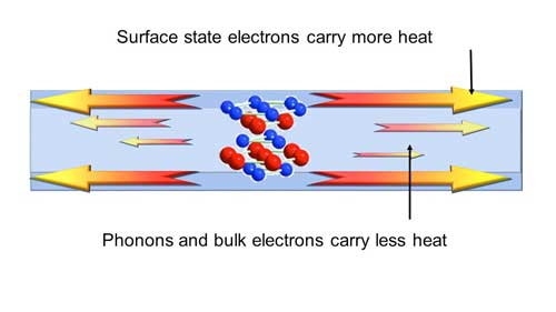
A very thin film has the ability to carry more heat on its surface than in the interior
A very thin film has the ability to carry more heat on its surface than in the interior. (Image: Xianfan Xu, Purdue University)
Past research has speculated that topological insulators could be useful for the development of spintronic devices, which encode information through the spins of electrons as opposed to electrical charge in today’s electronics.
The researchers found that the thinner the film is, the higher the heat conductivity. They also discovered that the ratio of thermal conductivity to electrical conductivity at the surface of the topological insulator materials can be more than 10 times higher than the Sommerfeld value, which is the value known for most metals and semiconductors determined by the Weidemann-Franz law. By conducting heat on just its surfaces rather than across the entire film, this material could prevent parts of a device from heating up or redirect heat.
Xu heat Purdue researchers have discovered a characteristic of this film that could help control heat flow in electronics. (Purdue University image/Jared Pike) Download image
Now, having identified this characteristic of heat transfer in topological insulators, the next step is to figure out how to use them for manipulating heat flow.
“There are not many ways to control heat. It’s not electricity, where you can turn it on and off,” Xu said. “But now there might be a chance to do that.”
The work is a collaborative effort among the research groups led by Xu, Yong Chen, a professor in Purdue’s Department of Physics and Astronomy, and Jesse Maassen, a physics professor at Dalhousie University in Canada.
Source: Purdue University

Explorarea proprietăților termoelectrice ale nanostructurilor de selenide din staniu(Exploring the thermoelectric properties of tin selenide nanostructures)

filmele subtiri SnSe nanostructurate pe care le-am fabricat au avut un factor de putere de doar ~ 5 la suta din cel de SnSe singur cristal la temperatura camerei”, a spus Shuhao Liu, un autor pe hartie. Dar, dupa ce au incercat o varietate de dopanti pentru a imbunatati factorul de putere al materialului, au stabilit ca „argintul a fost cel mai eficient – rezultand o imbunatatire a factorului de putere de 300 la suta fata de probele nedepuse”, a spus Liu. „Pelicula subțire nanostructurată dopată cu argint SnSe promite o valoare ridicată a meritelor.”Acest lucru face ca nanoflacile SnSe să se formeze pe suprafața plăcii. Adăugarea unui element dopant precum argintul la filmele subțiri SnSe în timpul sintezei materialelor poate optimiza în continuare proprietățile termoelectrice.

Posted: Mar 27, 2018

Exploring the thermoelectric properties of tin selenide nanostructures

(Nanowerk News) Single crystal tin selenide (SnSe) is a semiconductor and an ideal thermoelectric material; it can directly convert waste heat to electrical energy or be used for cooling. When a group of researchers from Case Western Reserve University in Cleveland, Ohio, saw the graphenelike layered crystal structure of SnSe, they had one of those magical “aha!” moments.

The group reports in the Journal of Applied Physics („Nanostructured SnSe: Synthesis, doping and thermoelectric properties”), that they immediately recognized this material’s potential to be fabricated in nanostructure forms. “Our lab has been working on two-dimensional semiconductors with layered structures similar to graphene,” said Xuan Gao, an associate professor at Case Western.
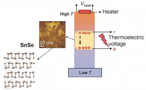
Electric charges in a nanostructured tin selenide (SnSe) thin film flow from the hot end to the cold end of the material and generate a voltage
Electric charges in a nanostructured tin selenide (SnSe) thin film flow from the hot end to the cold end of the material and generate a voltage. (Image: Xuan Gao)
Nanomaterials with nanometer-scale dimensions – such as thickness and grain size – have favorable thermoelectric properties. This inspired the researchers to grow nanometer-thick nanoflakes and thin films of SnSe to further study its thermoelectric properties.
The group’s work centers on the thermoelectric effect. They study how the temperature difference in a material can cause charge carriers – electrons or holes – to redistribute and generate a voltage across the material, converting thermal energy into electricity.
“Applying a voltage on a thermoelectric material can also lead to a temperature gradient, which means you can use thermoelectric materials for cooling,” said Gao. “Generally, materials with a high figure of merit have high electrical conductivity, a high Seebeck coefficient – generated voltage per Kelvin of temperature difference within a material – and low thermal conductivity,” he said.
A thermoelectric figure of merit, ZT, indicates how efficiently a material converts thermal energy to electrical energy. The group’s work focuses on the power factor, which is proportional to ZT and indicates a material’s ability to convert energy, so they measured the power factor of the materials they made.
To grow SnSe nanostructures, they used a chemical vapor deposition (CVD) process. They thermally evaporated a tin selenide powder source inside an evacuated quartz tube. Tin and selenium atoms react on a silicon or mica growth wafer placed at the low-temperature zone of the quartz tube. This causes SnSe nanoflakes to form on the surface of the wafer. Adding a dopant element like silver to SnSe thin films during material synthesis can further optimize its thermoelectric properties.
At the start, “the nanostructure SnSe thin films we fabricated had a power factor of only ~5 percent of that of single crystal SnSe at room temperature,” said Shuhao Liu, an author on the paper. But, after trying a variety of dopants to improve the material’s power factor, they determined that “silver was the most effective – resulting in a 300 percent power factor improvement compared to undoped samples,” Liu said. “The silver-doped SnSe nanostructured thin film holds promise for a high figure of merit.”
In the future, the researcher hope that SnSe nanostructures and thin films may be useful for miniaturized, environmentally friendly, low-cost thermoelectric and cooling devices.
Source: American Institute of Physics