Recoltarea energiei din fluctuațiile de lumină au dezvoltat o metodă și un material care generează un impuls electric atunci când lumina fluctuează de la soare la umbră și invers.

antenele, atunci când sunt încorporate în geamurile din sticlă, ar putea reduce zgomotele reci și ar economisi energie. Antenele, cu dimensiuni de ordinul zecilor de nanometri, reacționează la lumina apropiată de infraroșu și generează căldură.
Antenele sunt formate din discuri metalice mici, în acest caz nanodiscuri de aur, cu un diametru de 160 nm (0,16 micrometri). Ele sunt plasate pe un substrat și acoperite cu un film polimeric pentru a crea proprietățile piroelectrice.
„Nanoantenele pot fi fabricate pe suprafete mari, cu miliarde de discuri mici distribuite uniform pe suprafata
Aplicațiile care sunt mai aproape de mână pot fi găsite în cercetarea optică, cum ar fi detectarea luminii la scară nanometrică
Posted: Mar 26, 2018
Harvesting energy from light fluctuations
(Nanowerk News) It may in the future be possible to harvest energy with the aid of leaves fluttering in the wind. Researchers at the Laboratory of Organic Electronics at Linköping University have developed a method and a material that generate an electrical impulse when the light fluctuates from sunshine to shade and vice versa.
„Plants and their photosynthesis systems are continuously subjected to fluctuations between sunshine and shade. We have drawn inspiration from this and developed a combination of materials in which changes in heating between sunshine and shade generate electricity,” says Magnus Jonsson, docent and principal investigator for the research group in organic photonics and nano-optics at the Laboratory of Organic Electronics, Linköping University.
The results, which have been verified in both experiments and computer simulations, have been published in Advanced Optical Materials („Hybrid Plasmonic and Pyroelectric Harvesting of Light Fluctuations”).
Magnus Jonsson and Mina Shiran Chaharsoughi, Linköping University
This is Magnus Jonsson and Mina Shiran Chaharsoughi at the Laboratory of Organic Electronics, Linköping University. (Image: Thor Balkhed)
Together with researchers from the University of Gothenburg, Magnus Jonsson and his team have previously developed small nanoantennas that absorb sunlight and generate heat. They published an article together in Nano Letters in 2017, describing how the antennas when incorporated into window glass could reduce cold downdraughts and save energy. The antennas, with dimensions in the order of tens of nanometers, react to near infrared light and generate heat.
Mina Shiran Chaharsoughi, PhD student in Magnus Jonsson’s group, has now developed the technology further and created a tiny optical generator by combining the small antennas with a pyroelectric film.
„Pyroelectric” means that an electrical voltage develops across the material when it is heated or cooled. The change of temperature causes charges to move and the generation of an electric current in the circuit.
The antennas consist of small metal discs, in this case gold nanodiscs, with a diameter of 160 nm (0.16 micrometres). They are placed on a substrate and coated with a polymeric film to create the pyroelectric properties.
„The nanoantennas can be manufactured across large areas, with billions of the small discs uniformly distributed over the surface. The spacing between discs in our case is approximately 0.3 micrometres. We have used gold and silver, but they can also be manufactured from aluminium or copper,” says Magnus Jonsson.
The antennas generate heat that is then converted to electricity with the aid of the polymer. It is first necessary to polarize the polymer film in order to create a dipole across it, with a clear difference between positive and negative charge. The degree of polarisation affects the magnitude of the generated power, while the thickness of the polymer film seems not to have any effect at all.
„We force the polarisation into the material, and it remains polarised for a long time,” says Mina Shiran Chaharsoughi.
Mina Shiran Chaharsoughi carried out an experiment in order to demonstrate the effect clearly, holding a twig with leaves in the air flow from a fan. The motion of the leaves created sunshine and shade on the optical generator, which in turn produced small electrical pulses and powered an external circuit.
„The research is at an early stage, but we may in the future be able to use the natural fluctuations between sunshine and shade in trees to harvest energy,” says Magnus Jonsson.
Applications that are closer to hand can be found in optics research, such as the detection of light at the nanometre scale. Other applications may be found in optical computing.
Source: Linköping University

Textile electrice luminează o lampă atunci când sunt întinse(Electric textile lights a lamp when stretched)

Textilul constă din fire piezoelectrice țesute împreună cu fire conducătoare electric. Un fir piezoelectric este alcătuit din 24 de fibre, fiecare fiind subțire ca un fir de păr, fiecare fibră având un miez conductiv electric, înconjurat de un polimer izolator și piezoelectric. În timpul fabricării, țesătura este expusă unui câmp electric ridicat, care determină încărcarea pozitivă și negativă a polimerului într-un mod ordonat. Atunci când textilele sunt apoi întinse sau expuse la presiune, deformarea fibrelor determină o reorganizare a distribuției de sarcină, generând astfel o tensiune electrică. Firele conducătoare de electricitate sunt necesare pentru a forma un circuit închis prin care poate curge un curent electric.au dezvoltat o țesătură care transformă energia cinetică în energie electrică

Posted: Mar 22, 2018

Electric textile lights a lamp when stretched

(Nanowerk News) Working up a sweat from carrying a heavy load? That is when the textile works at its best. Researchers at Chalmers University of Technology have developed a fabric that converts kinetic energy into electric power, in cooperation with the Swedish School of Textiles in Borås and the research institute Swerea IVF. The greater the load applied to the textile and the wetter it becomes the more electricity it generates. The results are now published in the Nature Partner journal Flexible Electronics („Energy harvesting textiles for a rainy day: woven piezoelectrics based on melt-spun PVDF microfibres with a conducting core”).

Chalmers researchers Anja Lund and Christian Müller have developed a woven fabric that generates electricity when it is stretched or exposed to pressure. The fabric can currently generate enough power to light an LED, send wireless signals or drive small electric units such as a pocket calculator or a digital watch.
The technology is based on the piezoelectric effect, which results in the generation of electricity from deformation of a piezoelectric material, such as when it is stretched. In the study the researchers created a textile by weaving a piezoelectric yarn together with an electrically conducting yarn, which is required to transport the generated electric current.
„The textile is flexible and soft and becomes even more efficient when moist or wet,” Lund says. „To demonstrate the results from our research we use a piece of the textile in the shoulder strap of a bag. The heavier the weight packed in the bag and the more of the bag that consists of our fabric, the more electric power we obtain. When our bag is loaded with 3 kilos of books, we produce a continuous output of 4 microwatts. That’s enough to intermittently light an LED. By making an entire bag from our textile, we could get enough energy to transmit wireless signals.”
The piezoelectric yarn is made up of twenty-four fibres, each as thin as a strand of hair. When the fibres are sufficiently moist they become enclosed in liquid and the yarn becomes more efficient, since this improves the electrical contact between the fibres. The technology is based on previous studies by the researchers in which they developed the piezoelectric fibres, to which they have now added a further dimension.
„The piezoelectric fibres consist of a piezoelectric shell around an electrically conducting core,” Lund says. „The piezoelectric yarn in combination with a commercial conducting yarn constitute an electric circuit connected in series.”
Previous work by the researchers on piezoelectric textiles has so far mainly focused on sensors and their ability to generate electric signals through pressure sensitivity. Using the energy to continuously drive electronic components is unique.
„Woven textiles from piezoelectric yarns makes the technology easily accessible and it could be useful in everyday life. It’s also possible to add more materials to the weave or to use it as a layer in a multi-layer product. It requires some modification, but it’s possible,” Lund says.
The researchers consider that the technology is, in principle, ready for larger scale production. It is now mainly up to industrial product developers to find out how to make use of the technology. Despite the advanced technology underlying the material, the cost is relatively low and is comparable with the price of Gore-Tex. Through their collaboration with the Swedish School of Textiles in Borås the researchers have been able to demonstrate that the yarn can be woven in industrial looms and is sufficiently wear-resistant to cope with the harsh conditions of mass production.

More about: The textile that generates electricity

The textile consists of piezoelectric yarns woven together with electrically conducting yarns. A piezoelectric yarn is made up of 24 fibres each as thin as a strand of hair, with each fibre having an electrically conducting core surrounded by an insulating and piezoelectric polymer. During manufacture the fabric is exposed to a high electric field, which causes positive and negative charges in the polymer to be separated in an orderly manner. When the textile is then stretched or exposed to pressure, the deformation of the fibres causes a reorganisation of the charge distribution, thus generating an electrical voltage. The electrically conducting yarn is required to form a closed circuit through which an electric current can flow.

More about: The piezoelectric effect

The piezoelectric effect allows a material to generate an electrical voltage when it is exposed to pressure or stretching. Piezoelectricity is a result of a displacement of the charge distribution in the material due to deformation, and can be found in biological materials such as bone, protein and DNA and also in other types of materials such as ceramics, plastics and textiles.
Source: Chalmers University of Technology

Proiectarea unui material nou pentru îmbunătățirea ecografiei(Designing a new material for improved ultrasound)

Dezvoltarea unei baze teoretice pentru piezoelectricitatea ultrahighi in materialele feroelectrice a condus la un material nou cu dubla reactie piezoasa a oricarui ceramica feroelectrica comerciala existenta,Piezoelectricitatea este proprietatea materială în centrul ultrasunetelor medicale, al sonarului, al controlului activ al vibrațiilor și al multor senzori și actuatori. Datorită polarizării spontane, un material piezoelectric are capacitatea de a se deforma mecanic atunci când este aplicată o tensiune electrică sau de a genera sarcină electrică atunci când se aplică o forță mecanică.

Posted: Mar 21, 2018

Designing a new material for improved ultrasound

(Nanowerk News) Development of a theoretical basis for ultrahigh piezoelectricity in ferroelectric materials led to a new material with twice the piezo response of any existing commercial ferroelectric ceramics, according to an international team of researchers from Penn State, China and Australia.

Piezoelectricity is the material property at the heart of medical ultrasound, sonar, active vibration control and many sensors and actuators. Due to spontaneous polarization, a piezoelectric material has the ability to mechanically deform when an electric voltage is applied or to generate electric charge when a mechanical force is applied.
Adding small amounts of a carefully selected rare earth material, samarium, to a high-performance piezoelectric ceramic called lead magnesium niobate-lead titanate (PMN-PT) dramatically increases its piezo performance, the researchers report in Nature Materials(„Ultrahigh piezoelectricity in ferroelectric ceramics by design”). This materials-by-design strategy will be useful in designing materials for other applications as well, the team believes.
A long-range ferroelectric domain with nanoscale structure heterogeneity is evidenced by high-resolution TEM
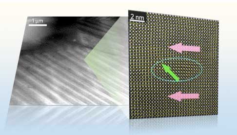
A long-range ferroelectric domain with nanoscale structure heterogeneity (4-8 nm) is evidenced by high-resolution TEM. (Image: Fei Li/Penn State)
“This is not the typical way to develop new materials,” said the team’s co-corresponding author, Long-Qing Chen, Donald W. Hamer Professor of Materials Science and Engineering, professor of mathematics and professor of engineering science and mechanics, Penn State. “The majority of existing useful materials are discovered by trial and error experiments. But here we designed and synthesized a new piezoelectric ceramic guided by theory and simulations.”
The team first analyzed the impact of adding various chemical dopants on the local structure of an existing ferroelectric ceramic. They were then able to select the most effective dopants by comparing the measured dielectric losses with the signatures obtained from phase-field simulations. After the screening of dopants, they then focused on the processing and composition optimization to achieve the ultrahigh piezoelectricity.
“This work is based on an understanding of the origin of ultrahigh piezoelectricity in the ferroelectric crystals that were developed 30 years ago. Our new understanding suggested that local structure heterogeneity plays an important role in piezoelectricity in ferroelectrics, which also can be extended to other functionalities,” said co-corresponding author Shujun Zhang, a professor of materials science formerly at Penn State and now at the University of Wollongong in Australia,
Local structure heterogeneity refers to nanoscale-size structural distortions within a host material created by doping a small amount of chemical species, in this case doping samarium in PMN-PT ceramics, as a way to modify the thermodynamic energy landscape of the material, which in turn increases the dielectric properties — the ability of a material to respond to an electrostatic field — and the piezoelectric effect.
“This material is a good choice to use in transducers, such as those used in medical ultrasound,” said lead author Fei Li, a research associate at Penn State. “We already have devices made from our material by a group at the University of Southern California.”
That device, called a needle transducer, uses a submillimeter piezoelectric element of the Penn State material, fitted into a standard needle or catheter, in order to perform minimally invasive procedures, to image inside the body or to guide precision surgery inside the body. The device has better performance than existing devices with the same dimensions, Li said.
The researchers have a provisional patent on this work.
Source: Penn State Materials Research Institute

Un viitor colorat luminat de fizica mistificatoare a semiconductorilor cu vopsea(

Unele materiale romantice care sună prea bine pentru a fi adevărate se dovedesc a fi adevărate și bune. O clasă emergentă de semiconductori, care ar putea lumina viitorul nostru cu culori nuanțate provenite din lasere, lămpi și chiar geamuri, ar putea fi ultimul exemplu.
Aceste materiale sunt foarte radiante, ușor de procesat din soluție și eficiente din punct de vedere energetic.Biexcitonii se ridică energic pentru a absorbi energia de intrare. Apoi se contractă energic și pompează lumina. Acest lucru ar funcționa nu numai la lasere, ci și la LED-uri sau alte suprafețe care utilizează materialul optoelectronic.

Posted: Mar 19, 2018

A future colorfully lit by mystifying physics of paint-on semiconductors

(Nanowerk News) Some novel materials that sound too good to be true turn out to be true and good. An emergent class of semiconductors, which could affordably light up our future with nuanced colors emanating from lasers, lamps, and even window glass, could be the latest example.

These materials are very radiant, easy to process from solution, and energy-efficient. The nagging question of whether hybrid organic-inorganic perovskites (HOIPs) could really work just received a very affirmative answer in a new international study led by physical chemists at the Georgia Institute of Technology.
Laser light in the visible range in a lab set-up
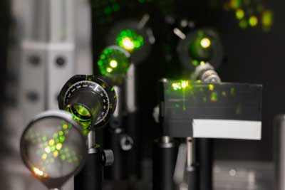
Laser light in the visible range is processed for use in the testing of quantum properties in materials in Carlos Silva’s lab at Georgia Tech. (Image: Allison Carter, Georgia Tech)
The researchers observed in an HOIP a “richness” of semiconducting physics created by what could be described as electrons dancing on chemical underpinnings that wobble like a funhouse floor in an earthquake. That bucks conventional wisdom because established semiconductors rely upon rigidly stable chemical foundations, that is to say, quieter molecular frameworks, to produce the desired quantum properties.
“We don’t know yet how it works to have these stable quantum properties in this intense molecular motion,” said first author Felix Thouin, a graduate research assistant at Georgia Tech. “It defies physics models we have to try to explain it. It’s like we need some new physics.”

Quantum properties surprise

Their gyrating jumbles have made HOIPs challenging to examine, but the team of researchers from a total of five research institutes in four countries succeeded in measuring a prototypical HOIP and found its quantum properties on par with those of established, molecularly rigid semiconductors, many of which are graphene-based.
“The properties were at least as good as in those materials and may be even better,” said Carlos Silva, a professor in Georgia Tech’s School of Chemistry and Biochemistry. Not all semiconductors also absorb and emit light well, but HOIPs do, making them optoelectronic and thus potentially useful in lasers, LEDs, other lighting applications, and also in photovoltaics.
The lack of molecular-level rigidity in HOIPs also plays into them being more flexibly produced and applied.
Silva co-led the study with physicist Ajay Ram Srimath Kandada. Their team published the results of their study on two-dimensional HOIPs in the journal Physical Review Materials („Stable biexcitons in two-dimensional metal-halide perovskites with strong dynamic lattice disorder”). Their research was funded by EU Horizon 2020, the Natural Sciences and Engineering Research Council of Canada, the Fond Québécois pour la Recherche, the Research Council of Canada, and the National Research Foundation of Singapore.

The ‘solution solution’

Commonly, semiconducting properties arise from static crystalline lattices of neatly interconnected atoms. In silicon, for example, which is used in most commercial solar cells, they are interconnected silicon atoms. The same principle applies to graphene-like semiconductors.
“These lattices are structurally not very complex,” Silva said. “They’re only one atom thin, and they have strict two-dimensional properties, so they’re much more rigid.”
“You forcefully limit these systems to two dimensions,” said Srimath Kandada, who is a Marie Curie International Fellow at Georgia Tech and the Italian Institute of Technology. “The atoms are arranged in infinitely expansive, flat sheets, and then these very interesting and desirable optoelectronic properties emerge.”
These proven materials impress. So, why pursue HOIPs, except to explore their baffling physics? Because they may be more practical in important ways.
“One of the compelling advantages is that they’re all made using low-temperature processing from solutions,” Silva said. “It takes much less energy to make them.”
By contrast, graphene-based materials are produced at high temperatures in small amounts that can be tedious to work with. “With this stuff (HOIPs), you can make big batches in solution and coat a whole window with it if you want to,” Silva said.

Funhouse in an earthquake

For all an HOIP’s wobbling, it’s also a very ordered lattice with its own kind of rigidity, though less limiting than in the customary two-dimensional materials.
“It’s not just a single layer,” Srimath Kandada said. “There is a very specific perovskite-like geometry.” Perovskite refers to the shape of an HOIPs crystal lattice, which is a layered scaffolding.
“The lattice self-assembles,” Srimath Kandada said, “and it does so in a three-dimensional stack made of layers of two-dimensional sheets. But HOIPs still preserve those desirable 2D quantum properties.”
Those sheets are held together by interspersed layers of another molecular structure that is a bit like a sheet of rubber bands. That makes the scaffolding wiggle like a funhouse floor.
“At room temperature, the molecules wiggle all over the place. That disrupts the lattice, which is where the electrons live. It’s really intense,” Silva said. “But surprisingly, the quantum properties are still really stable.”
Having quantum properties work at room temperature without requiring ultra-cooling is important for practical use as a semiconductor.
Going back to what HOIP stands for – hybrid organic-inorganic perovskites – this is how the experimental material fit into the HOIP chemical class: It was a hybrid of inorganic layers of a lead iodide (the rigid part) separated by organic layers (the rubber band-like parts) of phenylethylammonium (chemical formula (PEA)2PbI4).
The lead in this prototypical material could be swapped out for a metal safer for humans to handle before the development of an applicable material.

Electron choreography

HOIPs are great semiconductors because their electrons do an acrobatic square dance.
Usually, electrons live in an orbit around the nucleus of an atom or are shared by atoms in a chemical bond. But HOIP chemical lattices, like all semiconductors, are configured to share electrons more broadly.
Energy levels in a system can free the electrons to run around and participate in things like the flow of electricity and heat. The orbits, which are then empty, are called electron holes, and they want the electrons back.
“The hole is thought of as a positive charge, and of course, the electron has a negative charge,” Silva said. “So, hole and electron attract each other.”
The electrons and holes race around each other like dance partners pairing up to what physicists call an “exciton.” Excitons act and look a lot like particles themselves, though they’re not really particles.

Hopping biexciton light

In semiconductors, millions of excitons are correlated, or choreographed, with each other, which makes for desirable properties, when an energy source like electricity or laser light is applied. Additionally, excitons can pair up to form biexcitons, boosting the semiconductor’s energetic properties.
“In this material, we found that the biexciton binding energies were high,” Silva said. “That’s why we want to put this into lasers because the energy you input ends up to 80 or 90 percent as biexcitons.”
Biexcitons bump up energetically to absorb input energy. Then they contract energetically and pump out light. That would work not only in lasers but also in LEDs or other surfaces using the optoelectronic material.
“You can adjust the chemistry (of HOIPs) to control the width between biexciton states, and that controls the wavelength of the light given off,” Silva said. “And the adjustment can be very fine to give you any wavelength of light.”
That translates into any color of light the heart desires.
Source: By Ben Brumfield, Georgia Institute of Technology

Explozie lumina asupra misterului domului supraconductor(Shedding light on the mystery of the superconducting dome)

au indus supraconductivitatea într-un monostrat de disulfură de tungsten. Folosind un câmp electric în creștere, au fost capabili să arate cum se transformă materialul dintr-un izolator într-un superconductor și apoi din nou într-un izolator „reintrant”. Această descoperire ar putea deschide calea pentru proiectarea rațională a dispozitivelor superconductoare 2D care funcționează la temperaturi relativ ridicate.

Posted: Mar 19, 2018

Shedding light on the mystery of the superconducting dome

(Nanowerk News) University of Groningen physicists, and colleagues from Nijmegen and Hong Kong, have induced superconductivity in a monolayer of tungsten disulfide. By using an increasing electric field, they were able to show how the material turns from an insulator into a superconductor and then back into a ‘re-entrant’ insulator again. Their results show the typical ‘dome-shaped’ superconducting phase, and finally provide an explanation for this phenomenon.

The results were published in Proceedings of the National Academy of Sciences („Full superconducting dome of strong Ising protection in gated monolayer WS2„).
The scientists, led by University of Groningen associate professor Justin Ye, used an electric field to induce superconductivity in a monolayer of the semiconductor tungsten disulfide (WS2). In the initial state with very few carriers, the WS2 behaves as an insulator. ‘Basically, the electric field adds carriers to this normal band insulator, which increases the conductivity’, explains Ye. At low temperatures, this initiates a superconducting state.

Temperature

In the superconducting phase, the temperature at which superconductivity occurs rises as the electric field increases before dropping again. This kind of dome-shaped curve has been observed in many superconductors over several decades. It is one of the hallmarks of high temperature superconductors, many mysteries of which remain to be explained. A similar dome was recently also observed in several superconductors that were induced or controlled by field effect. What Ye and his colleagues observed was that, as the electric field increases even further, the system goes from superconductor back to insulator again.
‘This full range for the phase diagram, from insulator to superconductor and then to re-entry insulator, had never before been observed this clearly’, says Ye. ‘We managed it, because we worked with a truly 2D material and used ionic liquid to create an electric field that is much stronger than what is usually applied.’ Normally, as more carriers are added to a bulk or quasi-2D system, the electric field is eventually blocked. Ye: ‘But in a WS2 monolayer, our stronger field can still pass through, which is why we were able to observe the entire range and eventually reach the insulating phase.’

Counterintuitive

This allowed them to draw conclusions on why the different phases appear. ‘What we suggest is that the charge carriers in the material eventually become localized by the high electric field. Thus, they can no longer move through the material and it becomes an insulator.’ This is very counterintuitive, Ye adds: ‘People normally believe that higher gating means more carriers, hence more metallic behaviour.’ This discovery could pave the way for the rational design of 2D superconducting devices that function at relatively high temperatures. ‘Understanding is the first step to controlling the properties of materials for devices’, concludes Ye.
Source: University of Groningen

Borul poate forma o structură 2-D pură, de tip fagure, de tip grafen(Boron can form a purely honeycomb, graphene-like 2-D structure)

În plus, o latură de bor 2D de tip fagure poate permite comportamentul de superconductivitate. Deoarece în binecunoscutul supraconductor înalt Tc, MgB 2 , structura cristalină formată din avioane cu bor cu straturi intercalate Mg, unde planul bor are o structură de tip fagure curată ca grafen.Scanarea imaginilor de microscopie prin tuneluri (STM) dezvăluie o borofenă monolayer perfectă cu o latură plană, fără buclă fagure, similară cu grafenul. Calculele teoretice arată că borofenul de fagure pe Al (111) este stabil din punct de vedere energetic.

Posted: Mar 14, 2018

Boron can form a purely honeycomb, graphene-like 2-D structure

(Nanowerk News) Seeking for low-dimensional boron allotropes has attracted considerable interest in the past decades and tremendous theoretical works predict the existence of monolayer boron. As boron has only three valence electrons, the electron deficiency makes a honeycomb lattice of boron energetically unstable. Instead, a triangular lattice with periodic holes was predicted to be more stable.

In 2015, Prof. Wu has led a research team at Institute of Physics, Chinese Academy of Sciences, and successfully synthesized 2D borophene sheet on silver surface, which is exhibiting the predicted triangular lattice with different arrangements of hexagonal holes.
An intriguing question is whether it is possible to prepare a borophene monolayer with a pure honeycomb lattice. Honeycomb borophene will naturally host Dirac fermions and thus intriguing electronic properties resembling other group IV elemental 2D materials.
Additionally, a honeycomb 2D boron lattice may enable the superconductivity behavior. Since in the well-known high Tc superconductor, MgB2, the crystal structure consists of boron planes with intercalated Mg layers, where the boron plane has a pure honeycomb structure like graphene.
STM images of borophene monolayer with honeycomb lattice
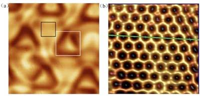
High resolution STM images of borophene monolayer with honeycomb lattice on Al(111). (© Science China Press)
It is remarkable that in MgB2, superconductivity occurs in the boron planes, while the Mg atoms serves as electron donors.
Recently, the research team led by Prof. Wu reported the successful preparation of a purely honeycomb, graphene-like borophene, by using an Al(111) surface as the substrate and molecular beam epitaxy (MBE) growth in ultrahigh vacuum (Science Bulletin, „xperimental Realization of Honeycomb Borophene”).
Scanning tunneling microscopy (STM) images reveal perfect monolayer borophene with planar, non-buckled honeycomb lattice similar as graphene. Theoretical calculations show that the honeycomb borophene on Al(111) is energetically stable.
Remarkably, nearly one electron charge is transferred to each boron atom from the Al(111) substrate and stabilizes the honeycomb borophene structure. This work vividly demonstrated that one can manipulate the borophene lattice by controlling the charge transfer between the substrate and the borophene. And the honeycomb borophene provides attractive possibility to construct boron-based atomic layers with unique electronic properties such as Dirac states, as well as to control superconductivity in boron-based compounds.
Source: Science China Press

Cercetătorii demonstrează existența unei noi forme de materie electronică

produs o demonstrație „la scară umană” a unei noi faze a materiei numite izolatoare topologice quadrupole, care a fost recent prevăzută cu ajutorul fizicii teoretice. Acestea sunt primele rezultate experimentale care au validat această teorie.am putut prezice existența acestei noi forme de materie, însă niciun material nu a fost găsit să aibă aceste proprietăți până acum”

Posted: Mar 14, 2018

Researchers demonstrate existence of new form of electronic matter

(Nanowerk News) Researchers have produced a „human scale” demonstration of a new phase of matter called quadrupole topological insulators that was recently predicted using theoretical physics. These are the first experimental findings to validate this theory.

The researchers report their findings in the journal Nature („A quantized microwave quadrupole insulator with topologically protected corner states”).
circuit board
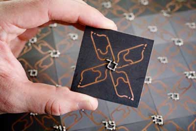
A single circuit board, foreground, that when joined with others forms the experimental array of the quadrupole topological insulator. (Image: L. Brian Stauffer)
The team’s work with QTIs was born out of the decade-old understanding of the properties of a class of materials called topological insulators. „TIs are electrical insulators on the inside and conductors along their boundaries, and may hold great potential for helping build low-power, robust computers and devices, all defined at the atomic scale,” said mechanical science and engineering professor and senior investigator Gaurav Bahl.
The uncommon properties of TIs make them a special form of electronic matter. „Collections of electrons can form their own phases within materials. These can be familiar solid, liquid and gas phases like water, but they can also sometimes form more unusual phases like a TI,” said co-author and physics professor Taylor Hughes .
TIs typically exist in crystalline materials and other studies confirm TI phases present in naturally occurring crystals, but there are still many theoretical predictions that need to be confirmed, Hughes said.
One such prediction was the existence of a new type of TI having an electrical property known as a quadrupole moment. „Electrons are single particles that carry charge in a material,” said physics graduate student Wladimir Benalcazar. „We found that electrons in crystals can collectively arrange to give rise not only to charge dipole units – that is, pairings of positive and negative charges – but also high-order multipoles in which four or eight charges are brought together into a unit. The simplest member of these higher-order classes are quadrupoles in which two positive and two negative charges are coupled.”
Multipoles
A dipole moment can be represented by two charges, one positive and one negative, separated in one dimension, a quadrupole moment can be represented by four charges separated in two dimensions, etc. (Image: Kitt Peterson)
It is not currently feasible to engineer a material atom by atom, let alone control the quadrupolar behavior of electrons. Instead, the team built a workable-scale analogue of a QTI using a material created from printed circuit boards. Each circuit board holds a square of four identical resonators – devices that absorb electromagnetic radiation at a specific frequency. The boards are arranged in a grid pattern to create the full crystal analogue.
„Each resonator behaves as an atom, and the connections between them behave as bonds between atoms,” said Kitt Peterson, the lead author and an electrical engineering graduate student. „We apply microwave radiation to the system and measure how much is absorbed by each resonator, which tells us about how electrons would behave in an analogous crystal. The more microwave radiation is absorbed by a resonator, the more likely it is to find an electron on the corresponding atom.”
The detail that makes this a QTI and not a TI is a result of the specifics of the connections between resonators, the researchers said.
„The edges of a QTI are not conductive like you would see in a typical TI,” Bahl said, „Instead only the corners are active, that is, the edges of the edges, and are analogous to the four localized point charges that would form what is known as a quadrupole moment. Exactly as Taylor and Wladimir predicted .”
„We measured how much microwave radiation each resonator within our QTI absorbed, confirming the resonant states in a precise frequency range and located precisely in the corners,” Peterson said. „This pointed to the existence of predicted protected states that would be filled by electrons to form four corner charges.”
Those corner charges of this new phase of electronic matter may be capable of storing data for communications and computing. „That may not seem realistic using our ‘human scale’ model,” Hughes said. „However, when we think of QTIs on the atomic scale, tremendous possibilities become apparent for devices that perform computation and information processing, possibly even at scales below that we can achieve today.”
The researchers said the agreement between experiment and prediction offered promise that scientists are beginning to understand the physics of QTIs well enough for practical use.
„As theoretical physicists, Wladimir and I could predict the existence of this new form of matter, but no material has been found to have these properties so far,” Hughes said. „Collaborating with engineers helped turn our prediction into reality.”
Source: University of Illinois at Urbana-Champaign

Noua conductoare MXene conducătoare poate debloca tehnologia biometrică și purtătoare a viitorului(New conductive MXene nanocoating may unlock biometric and wearable technology of the future)

dezvoltat un strat conductiv mecanic robust, care poate menține performanța în condiții de întindere și îndoire.Elementele electronice extensibile, flexibile și pliabile sunt esențiale pentru dezvoltarea unor tehnologii emergente cum ar fi afișajele adaptive, pielea artificială și dispozitivele biometrice și portabile. demonstrează că acoperirile MXene multistrat care pot suferi deformare mecanică la scară mare, menținând în același timp un nivel ridicat de conductivitate

Posted: Mar 09, 2018

New conductive MXene nanocoating may unlock biometric and wearable technology of the future

(Nanowerk News) A team of researchers from the College of Engineering at Texas A&M University have developed a mechanically robust conductive coating that can maintain performance under heavy stretching and bending.

Stretchable, bendable and foldable electronics are crucial for the development of emerging technologies like adaptive displays, artificial skin, and biometric and wearable devices. This presents a unique challenge of balancing electronic performance and mechanical flexibility. The difficulty lies in finding a material that can withstand a wide array of deformations, like stretching, bending and twisting, all while maintaining electrical conductivity. Adding to the challenge is the need for this conductivity to be engineered into a variety of different surfaces, such as cloth, fiber, glass or plastic.
Structural and Morphological Characterizations of MXene Multilayers
Figure 1. Structural and morphological characterizations of MXene multilayers. (A) Schematic of the PDAC/MXene LbL assembly process. Images of (B) immersion AQ48 and (C) spray assembly of multilayer coatings of varying number of layer pairs on glass. (D) A cross-sectional scanning electron microscopy (SEM) image of the mulAQ49 tilayer coating. (E) Ultraviolet-visible (UV-vis) spectra of MXene multilayers on glass. (F) Absorbance values at 770 nm versus number of layer pairs. a.u., arbitrary units. AQ50 (G) Growth profile of the multilayers on glass. (H) Root-mean-square (RMS) roughness versus number of layer pairs. (Image: H. An, T. Habib, S. Shah, H. Gao, M. Radovic, M. J. Green, J. L. Lutkenhaus) (click on image to enlarge)
A collaborative team from the Artie McFerrin Department of Chemical Engineering and the Department of Materials Science and Engineering led by Dr. Jodie Lutkenhaus , associate professor and holder of the William and Ruth Neely Faculty Fellowship, has solved this problem through the development of a new surface-agnostic stretchable, bendable and foldable conductive coating, opening the door for a wide variety of flexible electronics.
Two-dimensional metal carbides (MXenes) were chosen as the main focus of the research as previous research has shown them to have a metallic-like conductivity. The previous research on MXenes has focused primarily on the materials in the form of sheets. Although these sheets have the desired conductivity, they are not stretchable and their integration into different surfaces has not been shown.
Rather than using MXene sheets, the Texas A&M research team created MXene coatings through the sequential adsorption of negatively charged MXene sheets and positively charged polyelectrolytes using an aqueous assembly process known as layer-by-layer (LbL) assembly (See image 1-A).
The results of this process, described in depth in the latest issue of Science Advances („Surface-agnostic highly stretchable and bendable conductive MXene multilayers”), demonstrate that MXene multilayer coatings that can undergo large-scale mechanical deformation while maintaining a high level of conductivity (see video). The team has also successfully deposited the MXene multilayer coatings onto flexible polymer sheet, stretchable silicones, nylon fiber, glass and silicon.
Source: Texas A&M University

Axionul izolator prezintă o magnetorezistență gigantică la câmpuri magnetice scăzute(Axion insulator exhibits giant magnetoresistance at low magnetic fields)

Un material cuantic care prezintă o schimbare uriașă de rezistență la câmpurile magnetice relativ scăzute a fost fabricat de cercetători de la RIKEN, Universitatea din Tokyo și alte institute ( Science Advances , „Croitorie structură tricoloră de izolație topologică magnetică pentru izolator axion robust ” ). Materialul este promițător pentru realizarea circuitelor electronice în care curentul curge fără pierderi.Un material cuantic care a generat foarte mult entuziasm recent este izolatoarele topologice, care au proprietatea curioasă de a conduce electricitatea pe suprafețele lor, dar nu și în interiorul lor.

Posted: Mar 02, 2018

Axion insulator exhibits giant magnetoresistance at low magnetic fields

(Nanowerk News) A quantum material that exhibits a huge change in resistance at relatively low magnetic fields has been fabricated by researchers at RIKEN, the University of Tokyo and other institutes (Science Advances, „Tailoring tricolor structure of magnetic topological insulator for robust axion insulator”). The material is promising for realizing electronic circuits in which current flows without loss.

molecular beam epitaxy system
The molecular beam epitaxy system used to make an axion insulator device whose resistance varies greatly with applied magnetic field. (Image: RIKEN Center for Emergent Matter Science)
Quantum effects usually manifest themselves on an atomic or molecular scale, but they are observable on much larger scales in a special class of materials known as quantum materials. One quantum material that has been generating a lot of excitement recently is topological insulators, which have the curious property of conducting electricity on their surfaces but not in their interiors. Devices based on topological insulators will be more robust against internal defects and external conditions than conventional devices. Topological insulators also promise an array of exotic new carrier phenomena when symmetry rules are relaxed.

One such phenomenon is the topological magnetoelectric effect, in which the interior of a topological insulator is magnetized by a quantized current circulating on its surface. This effect has been difficult to observe experimentally because it has been challenging to find a suitable material system.

Masataka Mogi at the University of Tokyo and his collaborators had previously made a suitable system known as an axion insulator, but they observed axion insulator behavior only in a narrow range of magnetic fields.

Now, Mogi, with colleagues at the RIKEN Center for Emergent Matter Science and other institutions in Japan, has succeeded in making the axion insulator state more robust and useful by doping one magnetic ion into the bottom surface of their device and a different one into the top. This allowed them to individually reverse one surface magnetization at a time and observe how the axion insulator responds to a wider range of magnetic fields, electric fields and temperatures.

As a result, the researchers were able to observe a whopping change in the resistance of the system—over 10,000,000 per cent—with a small change in the applied magnetic field. While effects like this have been observed in other topological materials, they have usually required a much larger swing in the magnetic field.

This novel behavior may lead to new kinds of electronic devices, Mogi says. “Using contemporary spintronic techniques may enable us to construct dissipationless electronic circuits in which the edge current runs in parallel magnetization regions, but not in anti-parallel regions.”
Making practical devices will require increasing operating temperatures, which are currently capped below 1 kelvin. Mogi is confident that this can be accomplished by growing higher quality films.
Source: RIKEN

Wilele lui E. Coyote inspiră dezvoltarea unor noi proprietăți ale siliciului(Wile E. Coyote’s fall inspires development of new properties of silicon)

Rezultatele arată că siliciul poate avea un nou contract de închiriere a vieții, oferind noi modalități de a controla informațiile cu lumină, mai degrabă decât cu curent electric, ceea ce înseamnă computere mult mai rapide și comunicații cu o lățime de bandă mai mare

Posted: Feb 27, 2018

Wile E. Coyote’s fall inspires development of new properties of silicon

(Nanowerk News) An international team of scientists, led by the University

of Surrey, has discovered a new type of silicon that could be used to control light beams in a new kind of photonic chip – a chipset where information is carried by light beams rather than electrical currents.

The essence of the technology – where an object takes a moment to respond to the energy placed upon it – is a staple of cartoons such as Roadrunner, where characters run off cliffs and spend a moment in mid-air before falling.

Scientists hope that their discovery, detailed in a study published by Nature Photonics („Giant multiphoton absorption for THz resonances in silicon hydrogenic donors”), will lead to the development of more exciting technologies such as signal modulators for terahertz (THz) beams – which is part of the electromagnetic spectrum between visible/infrared light and radio/microwaves.

Silicon is widely used to send microwave signals for mobile communications, but it is very poor at sending visible light signals. The team discovered that the standard impurities that are sprinkled into ordinary computer chips to make transistors can control the flow of THz photons far more efficiently than almost anything else. This has the double benefit of potentially allowing a new method of chip-to-chip communication with silicon, currently only possible with much more expensive materials, but also pushing mobile communications to much higher frequency and allowing the transmission of more data.

The signal modulation effect works by using two or more photons, each of which could individually go straight through the silicon unhindered, and only when they arrive together they get absorbed. The first photon acts like a switch – its presence or absence determines what will happen to the others. The catch is that the second photon has to be almost simultaneous with the first, meaning that the intensity of the beams must be really high. The researchers tried using THz photons instead of the infrared photons used in all previous attempts, and found that they could get switching with thousands of times lower intensity than ever before.

Professor Ben Murdin from the University of Surrey, said: “It’s just like when Wile E. Coyote is chasing the Roadrunner and goes off the edge of a cliff – there’s always a moment before physics wakes up and realises he has too much potential energy and he falls. During this ‘coyote time’ (as gamers call it) sometimes something else can take effect like a rocket or a stone or a jump. That’s exactly how Heisenberg’s Uncertainty Principle works here – there’s a little bit of ‘coyote time’ after the first photon hits in which the molecule doesn’t know what energy it’s supposed to have, but the more energy it tries to ignore the less the coyote time available.

“We found that with terahertz light silicon’s coyote time is much, much longer, meaning this kind of photon switch is far more efficient than anything else we know of. The results show that silicon may have a completely new lease of life, providing new ways to control information with light rather than electrical current, meaning far faster computers and higher bandwidth communications.”

Source: University of Surrey

Nanocoarea inteligentă deschide ușa spre ferestrele inteligente(Clever nanocoating opens door to smart windows)

au dezvoltat un nou strat ultra-subțire care răspunde la căldură și frig, deschizând ușa spre „ferestrele inteligente”.

Vopseaua de auto-modificare, care este de o mie de ori mai subțire decât un fir de păr uman, funcționează automat, permițându-i să se încălzească automat când este rece și blocând razele soarelui atunci când este fierbinte.

Ferestrele inteligente au capacitatea de a regla în mod natural temperaturile din interiorul unei clădiri, ceea ce duce la beneficii majore pentru mediu și la economii semnificative.

Posted: Feb 26, 2018

Clever nanocoating opens door to smart windows

(Nanowerk News) Researchers from RMIT University in Melbourne Australia have developed a new ultra-thin coating that responds to heat and cold, opening the door to „smart windows”.

The self-modifying coating, which is a thousand times thinner than a human hair, works by automatically letting in more heat when it’s cold and blocking the sun’s rays when it’s hot.

Smart windows have the ability to naturally regulate temperatures inside a building, leading to major environmental benefits and significant financial savings.

Lead investigator Associate Professor Madhu Bhaskaran said the breakthrough will help meet future energy needs and create temperature-responsive buildings.

Mohammad Taha shows off an ultra-thin coating

Mohammad Taha shows off the ultra-thin coating developed at RMIT University. (Image: RMIT University)

„We are making it possible to manufacture smart windows that block heat during summer and retain heat inside when the weather cools,” Bhaskaran said.

„We lose most of our energy in buildings through windows. This makes maintaining buildings at a certain temperature a very wasteful and unavoidable process.

„Our technology will potentially cut the rising costs of air-conditioning and heating, as well as dramatically reduce the carbon footprint of buildings of all sizes.

„Solutions to our energy crisis do not come only from using renewables; smarter technology that eliminates energy waste is absolutely vital.”

Smart glass windows are about 70 per cent more energy efficient during summer and 45 per cent more efficient in the winter compared to standard dual-pane glass.

New York’s Empire State Building reported energy savings of US$2.4 million and cut carbon emissions by 4,000 metric tonnes after installing smart glass windows. This was using a less effective form of technology.

„The Empire State Building used glass that still required some energy to operate,” Bhaskaran said. „Our coating doesn’t require energy and responds directly to changes in temperature.”

Co-researcher and PhD student Mohammad Taha said that while the coating reacts to temperature it can also be overridden with a simple switch.

„This switch is similar to a dimmer and can be used to control the level of transparency on the window and therefore the intensity of lighting in a room,” Taha said. „This means users have total freedom to operate the smart windows on-demand.”

Windows aren’t the only clear winners when it comes to the new coating. The technology can also be used to control non-harmful radiation that can penetrate plastics and fabrics. This could be applied to medical imaging and security scans.

Bhaskaran said that the team was looking to roll the technology out as soon as possible.

„The materials and technology are readily scalable to large area surfaces, with the underlying technology filed as a patent in Australia and the US,” she said.

The research has been carried out at RMIT University’s state-of-the-art Micro Nano Research Facility with colleagues at the University of Adelaide and supported by the Australian Research Council.

Their findings have been published in Scientific Reports („Insulator–metal transition in substrate-independent VO2 thin film for phase-change devices”).

How the coating works

The self-regulating coating is created using a material called vanadium dioxide. The coating is 50-150 nanometres in thickness.

At 67 degrees Celsius, vanadium dioxide transforms from being an insulator into a metal, allowing the coating to turn into a versatile optoelectronic material controlled by and sensitive to light.

The coating stays transparent and clear to the human eye but goes opaque to infra-red solar radiation, which humans cannot see and is what causes sun-induced heating.

Until now, it has been impossible to use vanadium dioxide on surfaces of various sizes because the placement of the coating requires the creation of specialised layers, or platforms.

The RMIT researchers have developed a way to create and deposit the ultra-thin coating without the need for these special platforms – meaning it can be directly applied to surfaces like glass windows.

Source: RMIT University