Cristalele robotice care merg pe jos(Robotic crystals that walk n’roll)

Ei au dezvoltat cristale robotice care merg încet ca un vierme și se rostogolesc de 20.000 de ori mai repede decât viteza de mers pe jos. Aceste cristale organice în mișcare, au un potențial mare ca material pentru roboți moi în viitor, în special în domeniul medical.Cristalele noastre ar putea fi folosite ca un nou tip de material pentru roboți moi, cu o siguranță și confort îmbunătățite. În timp ce societatea noastră se îmbătrânește, trebuie să luăm în considerare relația simbiotică dintre oameni și roboți, deoarece roboții pot avea grijă de oameni, inclusiv de vârstnici, în viitorul apropiat „.

Posted: Feb 21, 2018

Robotic crystals that walk n’roll

(Nanowerk News) Scientists at Waseda University may have come a step closer to innovating soft robots to care for people. Its material, however, is something you may have never expected.

They have developed robotic crystals that walk slowly like an inchworm and roll 20,000 times faster than its walking speed. These autonomously moving, organic crystals have great potential as material for soft robots in the future, especially in the medical field.
soft robotics material
“The crystals are flexible, durable and lightweight,” says Hideko Koshima, a visiting professor at Waseda’s Research Organization for Nano & Life Innovation. “They could possibly be used as material for microrobots which transport substances in the microscopic region, for instance, carrying egg cells for infertility treatment or conducting invasive surgery.”
Their study was published in Nature Communications („Walking and rolling of crystals induced thermally by phase transition”).
Crystals have been expected to play an important role as locomotive material for soft robots, and its mechanical motion has been explored in terms of bending and expansion/contraction. However, more variety in movements was sought for.
Previously in 2016, Koshima’s research group reported that chiral azobenzene crystals, which were also used in the recent study, bend with exposure to light. During this investigation, the crystals were found to undergo phase transition at 145°C without fracturing, even after repeated heating and cooling.
soft robotics material
Based on these findings, they designed the robotic crystals demonstrating two different modes of locomotion: walking and rolling.
Using an infrared thermography camera and a digital optical microscope, the group observed that thin, long plate-like crystals with thickness gradient in the longitudinal direction walked slowly like an inchworm through repeated bending and straightening under heating and cooling cycles near the transition temperature on a hot plate, moving 1.5mm in 30 minutes. On the other hand, thinner, longer plate-like crystals with width gradient rolled 3.1mm in 0.2 seconds, accelerated by tilted bending then flipping, under only one process of heating and cooling.
“The driving force behind the walking and rolling locomotion was generated from the unsymmetrical shape of the crystals,” Koshima explains.
Although the scientists would need to further study how to precisely control the direction and speed of the robotic crystals for practical application, this finding opens a door to a new field of crystal robotics, and on a larger scale, brings us a step closer to addressing issues related to population aging.
“Currently, robots are rigid and heavy, making them unsuitable for daily interaction with humans,” points out Koshima. “Our crystals could be used as a new kind of material for soft robots with improved safety and comfort. As our society ages, we must consider the symbiotic relationship between humans and robots, since robots may look after people, including the elderly, in the near future.”
Koshima is now attempting to produce robotic crystals which undergo phase transition at a much lower temperature.
Source: Waseda University

Tuning surse de lumină cuantică(Tuning quantum light sources)

au modificat chimic tuburi mici de atomi de carbon. Aceste tuburi sunt primul material care emite fotoni singuri la temperatura camerei și lungimi de undă ale telecomunicațiilor. Nici un alt sistem de materiale nu a putut să îndeplinească simultan aceste două condiții critice de operare

Posted: Feb 21, 2018

Tuning quantum light sources

(Nanowerk News) Knowing the details of the quantum world—electrons and packets of light called photons—could radically improve computers and sensors. A critical component to making devices that harness the quantum world is a source that emits a regular stream of single photons.

Scientists at the Center for Integrated Nanotechnologies and their colleagues chemically modified tiny tubes of carbon atoms. These tubes are the first material to emit single photons at room temperature and telecom wavelengths. No other material system has been able to meet these two critical operational conditions simultaneously (Nature Photonics, „Tunable room-temperature single-photon emission at telecom wavelengths from sp3 defects in carbon nanotubes”).
The schematic shows the emission of a single photon (red) from a chemically modified carbon nanotube when excited by green light
The schematic shows the emission of a single photon (red) from a chemically modified carbon nanotube when excited by green light. (Image: Xiaowei He, Center for Integrated Nanotechnologies, Los Alamos)
This critical combination of features makes integrating devices that exploit the quantum world with existing optical networks a very real possibility. That is, the carbon nanotubes that allow for ultra secure data encryption could be used with today’s telecom network. The carbon nanotubes could also be integrated into devices for more sensitive sensors and future quantum computers.
The ability to integrate fiber-based quantum information technology into existing optical networks would be a significant step towards applications in quantum communication. To achieve this, quantum light sources must be able to emit single photons at telecommunication wavelengths and at room temperature.
This combination of features has been elusive until now, despite two decades of research efforts. Some systems (e.g., self-assembled quantum dots) emit at telecommunication wavelengths but require cryogenic cooling. Other systems (for example, diamond nitrogen-vacancy centers) operate at room temperature but can only emit in the visible spectral range.
Scientists at the Center for Integrated Nanotechnologies and their collaborators have produced functionalized carbon nanotubes that have both of these critical features. Carbon nanotubes had been previously identified as a promising quantum light source; however, the unstable photon emissions they generated were problematic.
The answer uncovered by scientists at the Center for Integrated Nanotechnologies was to chemically modify the nanotubes through aryl-diazonium reactions. This introduced defects to the nanotubes that allowed for controllable single-photon emission at both room temperature and telecommunication wavelengths. The team also demonstrated that the emission wavelength was tunable. Just as the tension and length of a violin string can be adjusted to achieve different frequencies, the diameter of the functionalized carbon nanotubes can be varied to generate different emission wavelengths.
Not only do these results have significance for basic science, including functionalization chemistry and quantum metrology, but they also open the door to exciting developments in quantum technologies.
Source: U.S. Department of Energy, Office of Science

Computerele ajută la descoperirea unui material nou, ieftin pentru a face LED-urile cu o calitate ridicată a culorilor(Computers aid discovery of new, inexpensive material to make LEDs with high color quality)

un nou material fosfor pentru LED-uri albe care este ieftin și ușor de făcut. Cercetatorii au construit prototipuri de becuri cu LED-uri albe, folosind noul fosfor. Prototipurile au avut o calitate mai bună a culorii decât multe LED-uri comerciale prezente pe piață.
Noul fosfor – realizat din elementele stronțiu, litiu, aluminiu și oxigen (o combinație denumită „SLAO”)

Posted: Feb 19, 2018

Computers aid discovery of new, inexpensive material to make LEDs with high color quality

(Nanowerk News) A team led by engineers at the University of California San Diego has used data mining and computational tools to discover a new phosphor material for white LEDs that is inexpensive and easy to make. Researchers built prototype white LED light bulbs using the new phosphor. The prototypes exhibited better color quality than many commercial LEDs currently on the market.

Researchers published the new phosphor on Feb. 19 in the journal Joule („Mining Unexplored Chemistries for Phosphors for High-Color-Quality White-Light-Emitting Diodes”).
SLAO Phosphor
Under UV light, the SLAO phosphor emits either green-yellow or blue light depending on the chemical activator mixed in. (Image: David Baillot/UC San Diego Jacobs School of Engineering)
Phosphors, which are substances that emit light, are one of the key ingredients to make white LEDs. They are crystalline powders that absorb energy from blue or near-UV light and emit light in the visible spectrum. The combination of the different colored light creates white light.
The phosphors used in many commercial white LEDs have several disadvantages, however. Many are made of rare-earth elements, which are expensive, and some are difficult to manufacture. They also produce LEDs with poor color quality.
Researchers at UC San Diego and Chonnam National University in Korea discovered and developed a new phosphor that avoids these issues. It is made mostly of earth-abundant elements; it can be made using industrial methods; and it produces LEDs that render colors more vividly and accurately.
The new phosphor–made of the elements strontium, lithium, aluminum and oxygen (a combination dubbed „SLAO”)–was discovered using a systematic, high-throughput computational approach developed in the lab of Shyue Ping Ong, a nanoengineering professor at the UC San Diego Jacobs School of Engineering and lead principal investigator of the study. Ong’s team used supercomputers to predict SLAO, which is the first known material made of the elements strontium, lithium, aluminum and oxygen. Calculations also predicted this material would be stable and perform well as an LED phosphor. For example, it was predicted to absorb light in the near-UV and blue region and have high photoluminescence, which is the material’s ability to emit light when excited by a higher energy light source.
LED Phosphor Color Quality Comparison
Untouched shots lit by (left) an LED containing a conventional phosphor and (right) a prototype LED containing the new SLAO phosphor. (Image: Yoon Hwa Kim and Wong Bin Im/Chonnam National University in Korea)
Researchers in the lab of Joanna McKittrick, a materials science professor at the Jacobs School of Engineering, then figured out the recipe needed to make the new phosphor. They also confirmed the phosphor’s predicted light absorption and emission properties in the lab.
A team led by materials science professor Won Bin Im at Chonnam National University in Korea optimized the phosphor recipe for industrial manufacturing and built white LED prototypes with the new phosphor. They evaluated the LEDs using the Color Rendering Index (CRI), a scale that rates from 0 to 100 how accurate colors appear under a light source. Many commercial LEDs have CRI values at around 80. LEDs made with the new phosphor yielded CRI values greater than 90.

The computational quest for a new material

Thanks to the computational approach developed by Ong’s team, discovery of the phosphor took just three months–a short time frame compared to the years of trial-and-error experiments it typically takes to discover a new material.
„Calculations are quick, scalable and cheap. Using computers, we can rapidly screen thousands of materials and predict candidates for new materials that have not yet been discovered,” Ong said.
Ong, who leads the Materials Virtual Lab and is a faculty member in the Sustainable Power and Energy Center at UC San Diego, uses a combination of high-throughput calculations and machine learning to discover next-generation materials for energy applications, including batteries, fuel cells and LEDs. The calculations were performed using the National Science Foundation’s Extreme Science and Engineering Discovery Environment at the San Diego Supercomputer Center.
In this study, Ong’s team first compiled a list of the most frequently occurring elements in known phosphor materials. To the researchers’ surprise, they found that there are no known materials containing a combination of strontium, lithium, aluminum and oxygen, which are four common phosphor elements. Using a data mining algorithm, they created new phosphor candidates containing these elements and performed a series of first-principles calculations to predict which would perform well as a phosphor. Out of 918 candidates, SLAO emerged as the leading material. It was predicted to be stable and exhibit excellent photoluminescence properties.
„It’s not only remarkable that we were able to predict a new phosphor compound, but one that’s stable and can actually be synthesized in the lab,” said Zhenbin Wang, a nanoengineering Ph.D. candidate in Ong’s research group and co-first author of the study.
The phosphor’s main limitation is its less than ideal quantum efficiency–how efficiently it converts incoming light to light of a different color–of about 32 percent. However, researchers note that it retains more than 88 percent of its emission at typical LED operating temperatures. In commercial LEDs, there’s usually a tradeoff with color quality, Ong noted. „But we want the best of both worlds. We have achieved excellent color quality. Now we are working on optimizing the material to improve quantum efficiency,” Ong said.
Source: University of California – San Diego

Sistemul captează puterea de la schimbările de temperatură zilnice(System draws power from daily temperature swings)

Noul sistem, numit un rezonator termic, ar putea permite funcționarea continuă, de ani de zile a sistemelor de teledetecție, de exemplu, fără a necesita alte surse de alimentare sau baterii, spun cercetătorii.echipa a creat o combinație de materiale adaptată cu atenție. Structura de bază este o spumă de metal, realizată din cupru sau nichel, care este apoi acoperită cu un strat de grafen pentru a asigura o conductivitate termică și mai mare. Apoi, spuma este infuzată cu un fel de ceară numită octadecan, un material cu schimbare de fază, care se schimbă între solid și lichid într-un anumit interval de temperatură ales pentru o anumită aplicație.

Posted: Feb 15, 2018

System draws power from daily temperature swings

(Nanowerk News) Thermoelectric devices, which can generate power when one side of the device is a different temperature from the other, have been the subject of much research in recent years. Now, a team at MIT has come up with a novel way to convert temperature fluctuations into electrical power. Instead of requiring two different temperature inputs at the same time, the new system takes advantage of the swings in ambient temperature that occur during the day-night cycle.

The new system, called a thermal resonator, could enable continuous, years-long operation of remote sensing systems, for example, without requiring other power sources or batteries, the researchers say.
The findings are being reported in the journal Nature Communications („Ultra-high thermal effusivity materials for resonant ambient thermal energy harvesting”), in a paper by graduate student Anton Cottrill, Carbon P. Dubbs Professor of Chemical Engineering Michael Strano, and seven others in MIT’s Department of Chemical Engineering.
System draws power from daily temperature swings
The team’s test device, which has been deployed on the roof of an MIT building for several months, was used to prove the principle behind their new energy-harvesting concept. The test device is the black box at right, behind a weather-monitoring system (white) and a set of test equipment to monitor the device’s performance (larger black case at left). (Image: Justin Raymond)
“We basically invented this concept out of whole cloth,” Strano says. “We’ve built the first thermal resonator. It’s something that can sit on a desk and generate energy out of what seems like nothing. We are surrounded by temperature fluctuations of all different frequencies all of the time. These are an untapped source of energy.”
While the power levels generated by the new system so far are modest, the advantage of the thermal resonator is that it does not need direct sunlight; it generates energy from ambient temperature changes, even in the shade. That means it is unaffected by short-term changes in cloud cover, wind conditions, or other environmental conditions, and can be located anywhere that’s convenient — even underneath a solar panel, in perpetual shadow, where it could even allow the solar panel to be more efficient by drawing away waste heat, the researchers say.
The thermal resonator was shown to outperform an identically sized, commercial pyroelectric material — an established method for converting temperature fluctuations to electricity — by factor of more than three in terms of power per area, according to Cottrill.
The researchers realized that to produce power from temperature cycles, they needed a material that is optimized for a little-recognized characteristic called thermal effusivity — a property that describes how readily the material can draw heat from its surroundings or release it. Thermal effusivity combines the properties of thermal conduction (how rapidly heat can propagate through a material) and thermal capacity (how much heat can be stored in a given volume of material). In most materials, if one of these properties is high, the other tends to be low. Ceramics, for example, have high thermal capacity but low conduction.
To get around this, the team created a carefully tailored combination of materials. The basic structure is a metal foam, made of copper or nickel, which is then coated with a layer of graphene to provide even greater thermal conductivity. Then, the foam is infused with a kind of wax called octadecane, a phase-change material, which changes between solid and liquid within a particular range of temperatures chosen for a given application.
A sample of the material made to test the concept showed that, simply in response to a 10-degree-Celsius temperature difference between night and day, the tiny sample of material produced 350 millivolts of potential and 1.3 milliwatts of power — enough to power simple, small environmental sensors or communications systems.
“The phase-change material stores the heat,” says Cottrill, the study’s lead author, “and the graphene gives you very fast conduction” when it comes time to use that heat to produce an electric current.
Essentially, Strano explains, one side of the device captures heat, which then slowly radiates through to the other side. One side always lags behind the other as the system tries to reach equilibrium. This perpetual difference between the two sides can then be harvested through conventional thermoelectrics. The combination of the three materials — metal foam, graphene, and octadecane — makes it “the highest thermal effusivity material in the literature to date,” Strano says.
While the initial testing was done using the 24-hour daily cycle of ambient air temperature, tuning the properties of the material could make it possible to harvest other kinds of temperature cycles, such as the heat from the on-and-off cycling of motors in a refrigerator, or of machinery in industrial plants.
“We’re surrounded by temperature variations and fluctuations, but they haven’t been well-characterized in the environment,” Strano says. This is partly because there was no known way to harness them.
Other approaches have been used to try to draw power from thermal cycles, with pyroelectric devices, for example, but the new system is the first that can be tuned to respond to specific periods of temperature variations, such as the diurnal cycle, the researchers say.
These temperature variations are “untapped energy,” says Cottrill, and could be a complementary energy source in a hybrid system that, by combining multiple pathways for producing power, could keep working even if individual components failed. The research was partly funded by a grant from Saudi Arabia’s King Abdullah University of Science and Technology (KAUST), which hopes to use the system as a way of powering networks of sensors that monitor conditions at oil and gas drilling fields, for example.
“They want orthogonal energy sources,” Cottrill says — that is, ones that are entirely independent of each other, such as fossil fuel generators, solar panels, and this new thermal-cycle power device. Thus, “if one part fails,” for example if solar panels are left in darkness by a sandstorm, “you’ll have this additional mechanism to give power, even if it’s just enough to send out an emergency message.”
Such systems could also provide low-power but long-lasting energy sources for landers or rovers exploring remote locations, including other moons and planets, says Volodymyr Koman, an MIT postdoc and co-author of the new study. For such uses, much of the system could be made from local materials rather than having to be premade, he says.
This approach “is a novel development with a great future,” says Kourosh Kalantar-zadeh, a distinguished professor of engineering at RMIT University in Melbourne, Australia, who was not involved in this work. “It can potentially play an unexpected role in complementary energy harvesting units.”
He adds, “To compete with other energy harvesting technologies, always higher voltages and powers are demanded. However, I personally feel that it is quite possible to gain a lot more out of this by investing more into the concept. … It is an attractive technology which will be potentially followed by many others in the near future.”
Source: By David L. Chandler, MIT

Pătură de cauciuc la un nivel atomic(Rubber blanket at an atomic level)

Materialele bidimensionale, cum ar fi grafenul, care constau doar din unul sau mai multe straturi atomice, au fost un aspect foarte promițător al științei materialelor în ultimii ani. Acestea demonstrează proprietăți remarcabile care deschid posibilități tehnice complet noi, de la tehnologia senzorilor la celulele solare.
Cu toate acestea, există un fenomen important care nu a putut fi măsurat cu exactitate până în prezent: stresul și presiunea internă extremă pe care pot fi supuse astfel de materiale, care modifică adesea drastic proprietățile fizice ale materialului.

Posted: Feb 12, 2018

Rubber blanket at an atomic level

(Nanowerk News) Two-dimensional materials such as graphene, which consist of only one or a few atomic layers, have been a very promising aspect of materials science over recent years. They demonstrate remarkable properties that open up completely new technical possibilities, from sensor technology to solar cells.

However, there is one important phenomenon that could not be measured accurately up until now: the extreme internal stresses and strains that such materials may be subjected to, which often drastically alter the material’s physical properties. TU Wien has now successfully measured these distortions in 2D materials at microscopic level, which means it is now possible to observe precisely (point for point) how the properties of a material may be altered as a result of a simple distortion. These new measurement methods have now been published in the specialist journal Nature Communications („Optical imaging of strain in two-dimensional crystals”).
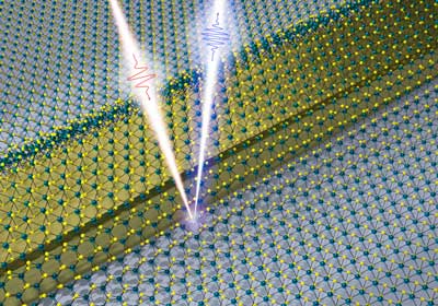
measuring distortions in 2D materials
The basic idea of the measurement method: red light hits the surface – blue light is sent back. (Image: TU Vienna)

Stretching and compression

When a material is stretched or compressed, the distance between the individual atoms changes, and this distance has an influence on the electronic properties of the material. This phenomenon has been used in semiconductor technology for years: silicon crystals, for example, can be grown so that they are permanently under internal mechanical stress.
However, two-dimensional materials, which consist only of an ultra-thin layer, offer much greater potential: „A crystal can be stretched by perhaps one percent before it breaks. With 2D materials, deformation of ten or twenty percent is possible”, says Prof. Thomas Müller from the Photonics Institute (Faculty of Electrical Engineering and Information Technology) at TU Wien. Depending on the deformation and mechanical stresses present within the material, the electronic properties may completely change, such as the ability of the electrons to absorb incoming light.
„Up until now, if you wanted to measure stresses present in this type of material you had to rely on extremely complicated measurement methods”, explains Lukas Mennel (TU Wien), lead author of the publication. For example, you could observe the surface using a transmission electron microscope, measure the average distance between the atoms and then deduce any stretching or compression from that. At TU Wien, this process has now been made much simpler and more accurate.

Red light in, blue light out

Here, a remarkable effect called frequency doubling is used: „If you irradiate specific materials – in our case a layer of molybdenum disulphide – with a suitable laser beam, the material may reflect back light of a different colour”, explains Thomas Müller. Two photons in the incoming laser beam are combined to form one photon with double the energy, which is emitted from the material.
However, the intensity of this effect depends on the internal symmetry of the material. Usually, molybdenum disulphide has a honeycomb-like structure, i.e. hexagonal symmetry. If the material is stretched or compressed, this symmetry is slightly distorted – and this small distortion has a dramatic effect on the intensity of the light reflected back from the material.
If you place a layer of molybdenum disulphide over a microstructure, like putting a rubber blanket over a climbing frame, the result is a complex pattern of local distortions. You can now use a laser to scan the material point for point and thus obtain a detailed map of these stretches and compressions. „In doing so, not only can we measure the severity of these deformations, but we can also see the exact direction in which they run”, explains Lukas Mennel.
These imaging methods can now be used for the local, targeted adjustment of material properties. „For example, custom material deformations in solar cells could ensure that free charge carriers are diffused away in the right direction as quickly as possible”, says Thomas Müller. This research on 2D materials means that a new, powerful tool is now available.
Source: Vienna University of Technology

Super-adsorbant MOF pentru a controla umiditatea(Super-adsorbent MOF to control humidity)

Materialul nostru super-adsorbant are proprietăți unice”, explică Alezi. Două realizări descoperite cu noul MOF (Cr-soc-MOF-1) sunt stabilitatea sa în apă, spre deosebire de multe MOF foarte poroase și porii interni de capacitate mare care pot adsorbi de două ori greutatea MOF ca apă ( vezi imaginea). O altă trăsătură vitală este reversibilitatea ușoară a absorbției apei. Apa adsorbită atunci când nivelurile de umiditate sunt ridicate pot fi eliberate imediat când umiditatea scade. Acest lucru oferă un material ideal pentru controlul umidității în spații restrânse.Acest material nou este un singur produs al angajamentului pe termen lung al lui Eddaoudi de a explora capacitățile MF. „Din cele mai bune cunoștințe, noul nostru MOF de absorbție a apei depășește toate MOF existente în ceea ce privește capacitatea, reversibilitatea și performanța ciclică”, spune Eddaoudi.

Posted: Feb 05, 2018

Super-adsorbent MOF to control humidity

(Nanowerk News) Humidity control is a vital aspect of air conditioning, but high energy requirements make conventional methods expensive and environmentally damaging. Researchers at KAUST have developed a metal-organic framework (MOF) that, within its range of applications, could control humidity in an eco-friendly and cost-effective way (Chem, „Reticular chemistry in action: A hydrolytically stable MOF capturing twice its weight in adsorbed water”).

The crystal structure of the super-adsorbent Cr-soc-MOF-1
The crystal structure of the super-adsorbent Cr-soc-MOF-1, hosting twice its weight as adsorbed water within its extensive network of micropores. The framework is represented in green, red and grey, and water molecules are represented with blue spheres. (Image: Mohamed Eddaoudi)
MOFs encompass metal centers or clusters held in a porous framework by organic linker groups. The key to designing a MOF with specific properties is the ability to control the size and chemical structure of the pores by varying the metal and organic parts within each framework.
Dalal Alezi works in Mohamed Eddaoudi’s research group at KAUST where a wide range of MOFs are being developed for gas separation, purification and chemical catalysis. This work is part of her doctoral research.
„Our super-adsorbent material has unique properties,” explains Alezi. Two breakthrough achievements with the new water-adsorbing MOF (Cr-soc-MOF-1) are its stability in water, unlike many highly porous MOFs, and its high-capacity internal pores that can adsorb twice the weight of the MOF as water (see image). Another vital feature is the easy reversibility of the water uptake. The water adsorbed when humidity levels are high can readily be released when the humidity falls. This yields an ideal material for controlling humidity in restricted spaces.
„Regulating escalating humidity levels, especially indoors and in confined environments, such as aircraft cabins and air-conditioned buildings, is a critical challenge,” says Youssef Belmabkhout, a senior research scientist in Eddaoudi’s group. He adds: „The conventional systems consume large amounts of energy, require intricate design and excessive cost.”
This new material is just one product of Eddaoudi’s long-term commitment to exploring the capabilities of MOFs. „To the best of our knowledge our new water-adsorbing MOF outperforms all existing MOFs in terms of capacity, reversibility and cyclic performance,” says Eddaoudi. The easy reversibility will be crucial for commercial applications. The team have already maintained the exceptional water uptake and release through more than 100 adsorption-desorption cycles.
Eddaoudi also emphasizes that water-adsorbing MOFs are ready to provide effective solutions to challenges other than regulating humidity, such as tackling water scarcity and environmental sustainability in energy-efficient ways. Possibilities include harvesting drinkable water from air and use in water desalination and purification.
The researchers are now working to scale up their water-adsorbing materials in order to demonstrate commercial potential and move into real-world applications.
Source: King Abdullah University of Science and Technology

Luarea energiei solare la margine(Taking solar energy to the edge)

au descoperit o modalitate eficienta de a face panouri solare combinate si dispozitive de emisie de lumina. Mai degrabă decât folosind blocuri de materiale pervoskit hibride, au stratificat mai multe foi subțiri unul peste altul ( Stiinta , „extrem de eficient de disociere a excitonilor interne prin stări de margine în perovskiti 2D stratificate“ și Știință , „Pornesc perovskit Photoresponse“ ).
În acest nou model stratificat, au descoperit importante „stări de margine a stratului”. În aceste stări, energia este foarte conservată. Când este excitat de lumină sau de alte surse, materialul produce energie care nu se disipează instantaneu și poate fi utilizată pentru a încărca bateriile sau pentru a face alte lucrări. Aceasta înseamnă că creează un transportator de lungă durată, gratuit, care poate fi recoltat și manipulat.Hibridele perovskite reprezintă o nouă clasă de materiale cu costuri reduse care pot capta și emite lumină. Acest material poate fi sintetizat în mai multe forme: structuri 3-D în vrac, foi de cristal 2-D și tije 1-D. În particular, compușii stratificați pot fi creați prin stivuirea foilor de cristal 2-D cu straturi organice subțiri între ele.
În comparație cu variantele 3-D în vrac, aceste foi de perovskite sunt stabile intrinsec și reglabile pe scară largă. Prin urmare, aceste foi subțiri pot avea aplicații largi într-o varietate de tehnologii.

Posted: Feb 05, 2018

Taking solar energy to the edge

(Nanowerk News) At the Center for Integrated Nanotechnology (CINT), researchers discovered an efficient way to make combined solar panels and light-emitting devices. Rather than using blocks of hybrid perovskite materials, they layered several thin sheets on top of each other (Science, „Extremely efficient internal exciton dissociation through edge states in layered 2D perovskites”and Science, „Powering up perovskite photoresponse”).

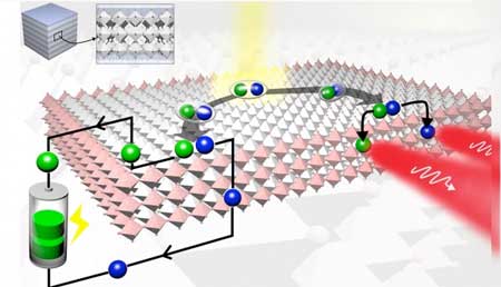
In this new layered pattern, they discovered important “layer-edge states.” In these states, energy is highly conserved. When excited by light or other sources, the material produces energy that doesn’t instantly dissipate and can be used to charge batteries or do other work. That is, it creates long-lived, free charge carriers that can be harvested and manipulated.
An artistic rendering shows the dissociation of electron-hole pairs to free carriers at crystal edges resulting in efficient solar energy and light emission
An artistic rendering shows the dissociation of electron-hole pairs (excitons) to free carriers at crystal edges resulting in efficient solar energy (>12 percent) and light emission (>30 percent). Dissociated carriers captured and located at the edges have lower energy and last longer. (Image: Jean-Christophe Blancon, Los Alamos National Laboratory)
Compared to blocks of material, layered sheets of perovskites offer a host of benefits. The sheets are more chemically stable, more environmentally friendly, and more tunable to fit the needs of new applications or experiments. Discovery of edge states opens new avenues for designing and fabricating efficient electronic devices which collect and emit light. These devices include low-cost solar cells, LEDs, laser diodes, and detectors.
Hybrid perovskites are a new class of low-cost materials that can capture and emit light. This material can be synthesized in several forms: bulk 3-D structures, 2-D crystal sheets, and 1-D rods. In particular, layered compounds can be created by stacking 2-D crystal sheets with thin organic layers in between.
Compared to bulk 3-D variations, these sheets of perovskites are intrinsically stable and widely tunable. Therefore, these thin sheets may have broad applications in a variety of technologies.
In this study, scientists from CINT as well as international collaborators describe a strategy to layer sheets of 2-D perovskites to drastically enhance the material’s optoelectronic properties. They found that in materials with three or more layers, charged particles (electrons and holes) become trapped at low-energy states near the edge of the crystal layers.
These carriers exhibit a 5-fold increase in their lifetime and do not lose energy to heat, resulting in tremendous improvements in efficiency for light-capturing devices.
On the flip side, devices that emit light are also tremendously more effective because trapped carriers can recombine very efficiently.
These results address a long-standing problem not just for the perovskite family but also for a large group of materials. Often, the edges and surface states of materials can degrade the optoelectronic properties.
Now, the structure of these materials can be chemically designed and engineered to achieve efficient flow of charge and energy leading to high-efficiency optoelectronic devices.
Source: U.S. Department of Energy, Office of Science

Dioxid de vanadiu: Un material revoluționar pentru electronica de mâine(Vanadium dioxyde: A revolutionary material for tomorrow’s electronics)

O caracteristică cheie a acestui compus este că se comportă ca un izolator la temperatura camerei, dar ca un conductor la temperaturi de peste 68 ° C. Acest comportament, cunoscut și sub numele de tranziția izolatoarelor metalice, este studiat într-un proiect ambițios al UE Orizont 2020 numit Switch Phase-Change. EPFL a fost aleasă pentru a coordona proiectul în urma unui proces de selecție provocator.

Posted: Feb 05, 2018

Vanadium dioxyde: A revolutionary material for tomorrow’s electronics

(Nanowerk News) First came the switch. Then the transistor. Now another innovation stands to revolutionize the way we control the flow of electrons through a circuit: vanadium dioxide (VO2). A key characteristic of this compound is that it behaves as an insulator at room temperature but as a conductor at temperatures above 68°C. This behavior – also known as metal-insulator transition – is being studied in an ambitious EU Horizon 2020 project called Phase-Change Switch. EPFL was chosen to coordinate the project following a challenging selection process.

Vanadium Dioxide Chip
This is a Vanadium Dioxide chip developed at EPFL’s NANOLAB. (Image: Jamani Caillet, EPFL)
The project will last until 2020 and has been granted €3.9 million of EU funding. Due to the array of high-potential applications that could come out of this new technology, the project has attracted two major companies – Thales of France and the Swiss branch of IBM Research – as well as other universities, including Max-Planck-Gesellschaft in Germany and Cambridge University in the UK. Gesellschaft für Angewandte Mikro- und Optoelektronik (AMO GmbH), a spin-off of Aachen University in Germany, is also taking part in the research.
Scientists have long known about the electronic properties of VO2 but haven’t been able to explain them until know. It turns out that its atomic structure changes as the temperature rises, transitioning from a crystalline structure at room temperature to a metallic one at temperatures above 68°C. And this transition happens in less than a nanosecond – a real advantage for electronics applications.
„VO2 is also sensitive to other factors that could cause it to change phases, such as by injecting electrical power, optically, or by applying a THz radiation pulse,” says Adrian Ionescu, the EPFL professor who heads the school’s Nanoelectronic Devices Laboratory (Nanolab) and also serves as the Phase-Change Switch project coordinator.

The challenge: reaching higher temperatures

However, unlocking the full potential of VO2 has always been tricky because its transition temperature of 68°C is too low for modern electronic devices, where circuits must be able to run flawlessly at 100°C.
But two EPFL researchers – Ionescu from the School of Engineering (STI) and Andreas Schüler from the School of Architecture, Civil and Environmental Engineering (ENAC) – may have found a solution to this problem, according to their joint research published in Applied Physics Letters in July 2017. They found that adding germanium to VO2 film can lift the material’s phase change temperature to over 100°C.
Even more interesting findings from the Nanolab – especially for radiofrequency applications – were published in IEEE Access („Vanadium Oxide bandstop tunable filter for Ka frequency bands based on a novel reconfigurable spiral shape defected ground plane CPW”).
For the first time ever, scientists were able to make ultra-compact, modulable frequency filters. Their technology also uses VO2 and phase-change switches, and is particularly effective in the frequency range crucial for space communication systems (the Ka band, with programmable frequency modulation between 28.2 and 35 GHz).

Neuromorphic processors and autonomous vehicles

These promising discoveries are likely to spur further research into applications for VO2 in ultra-low-power electronic devices. In addition to space communications, other fields could include neuromorphic computing and high-frequency radars for self-driving cars.
Source: Ecole Polytechnique Fédérale de Lausanne

Noile materiale MXene ar putea capta energia de frecare risipită de la telefoanele inteligente(

carburile metalice de tranziție, cunoscute sub numele de MXenes, ar putea fi folosite pentru recoltarea energiei de frecare pierdute, de exemplu, din contracțiile musculare în timpul tipăririi sau mersului pe jos.MXenes, descoperit în 2011, cuprinde una dintre cele mai mari familii de materiale bidimensionale. Acestea au o conductivitate electrică ridicată și capacitatea de absorbție a electronilor în contact cu polimerii și alte materiale. Această combinație neobișnuită de proprietăți face MXenes util ca componente pentru nanogeneratoarele triboelectrice (TENG), care transformă mișcările musculare în energie electrică. Studiul sugerează că aceste materiale avansate ar putea fi încorporate în telefoane mobile, dispozitive electronice portabile, dispozitive portabile și laptop-uri, ceea ce le va face în cele din urmă să se autodeclamă.

Posted: Feb 01, 2018

New MXene materials could capture wasted frictional energy from smartphones

(Nanowerk News) Imagine that every time you tapped out a message on your smartphone, it would create electric power instead of sapping your phone’s battery. That scenario could one day be a reality, according to a researcher at Missouri University of Science and Technology.

Writing in the February 2018 issue of the journal Nano Energy („Metallic MXenes: A New Family of Materials for Flexible Triboelectric Nanogenerators”), Dr. Vadym Mochalin, associate professor of chemistry at Missouri S&T, describes how a new family of two-dimensional transition metal carbides, known as MXenes, could be used to harvest wasted frictional energy, for example, from muscle contractions during typing or walking.
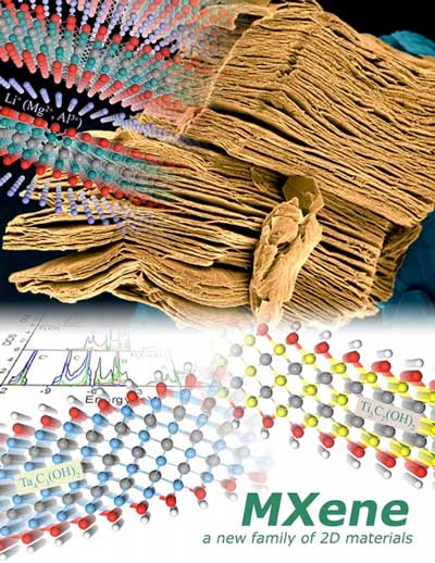
scanning electron microphotograph of Ti3C2 MXene flake
Artistic representation of scanning electron microphotograph of Ti3C2 MXene flake, superimposed with atomistic models of several MXenes and electronic density of states calculated using these models. (Image: Vadym Mochalin)
MXenes, discovered in 2011, comprise one of the largest families of two-dimensional materials. They possess high electrical conductivity and the ability to uptake electrons when in contact with polymers and other materials. This unusual combination of properties makes MXenes useful as components for triboelectric nanogenerators (TENG), which turn muscle movements into electric power. The research suggests these advanced materials could be incorporated into mobile phones, handheld electronics, wearable devices and laptops, ultimately making them self-powering.
“Exploring new chemistries and fundamental physical properties of MXenes for applications in energy storage, biology and medicine, electronics, composites, sensors and water purification is a hot area in the two-dimensional materials field,” says Mochalin.
The paper was written in collaboration with research groups from Drexel and Clemson universities.
Another study from Mochalin and his collaborators, “Saturable Absorption in 2D Ti3C2 MXene Thin Films for Passive Photonic Diodes,” was published in Advanced Materials („Saturable Absorption in 2D Ti3C2 MXene Thin Films for Passive Photonic Diodes”). This research shows how the non-linear optical properties of MXene – fullerene layered structures enable light rectification, a process similar to electrical current rectification which has been in use in electronics for decades. When compared to other two-dimensional materials, such as graphene, MXene is superior in its mechanical stability, conductivity and light radiation damage resistance, the researchers write.
A technique developed by Mochalin’s research group to deposit the nearly transparent and conductive MXene films on glass and other substrates may be used to fabricate passive saturable absorbers for generation of nanosecond pulses of high energy and peak power with solid-state bulk lasers. The high-energy ultrafast laser pulses are beneficial for processing materials where thermal influence must be minimized, for example, in drilling and cutting metals, delicate semiconductor wafers, polymeric stents, glasses, and other materials. These MXene films — only tens of nanometers in thickness — are also ideal for a wide range of applications in photonics, photovoltaics, flexible electronics, environment- and photo-sensitive sensors, and many others.
“MXenes are relatively young but already have captured a great deal of attention from scientists,” Mochalin says. “As we explore new synthetic routes to MXenes and study their fundamental physical and chemical properties, as well as their vibrational properties using Raman spectroscopy and neutron scattering, we become more and more excited about the future of MXenes. Why? Because we realize how much this family of materials has yet to offer to help us meet important societal challenges — from energy to healthcare — and to revolutionize our everyday lives.”
Working with international scholars, Mochalin’s research group at Missouri S&T leads the studies on the synthesis, characterization, computational modeling, and development of novel nanomaterials, like MXenes and nanodiamonds, for energy storage systems, composites, and biomedical applications. Mochalin involves Missouri S&T chemistry students in research — from highly-motivated undergraduates, to post-doctoral researchers. He has obtained six patents for discoveries in the fields of nanodiamonds, biodegradable composite materials, and energy storage.
Source: Missouri University of Science and Technology

2-D staniu fără flambaj: Un posibil izolator topologic(2-D tin without buckling: A possible topological insulator)

Planar stanene are perspective extraordinare în domeniul electronicii și calculului. „Efectul QSH este destul de delicat, iar cei mai mulți izolatori topologici îl arată doar la temperaturi scăzute”, spune liderul echipei de proiect Guy Le Lay de la Universitatea Aix-Marseille. „Cu toate acestea, stanenul este prevăzut să adopte o stare QSH chiar și la temperatura camerei și mai sus, mai ales atunci când funcționează cu alte elemente.În viitor, sperăm să vedem stanene partenere cu silicen în circuitele de calculatoare.Această combinație ar putea accelera drastic eficiența computațională , chiar și în comparație cu tehnologia de vârf.

Posted: Jan 19, 2018

2-D tin without buckling: A possible topological insulator

(Nanowerk News) Sometimes it pays to be two-dimensional. The merits of graphene, a 2D sheet of carbon atoms, are well established. In its wake have followed a host of „post-graphene materials” – structural analogues of graphene made of other elements like silicon or germanium.

Now, an international research team led by Nagoya University (Japan) involving Aix-Marseille University (France), the Max Planck Institute in Hamburg (Germany) and the University of the Basque country (Spain) has unveiled the first truly planar sample of stanene: single sheets of tin (Sn) atoms. Planar stanene is hotly tipped as an extraordinary electrical conductor for high technology.
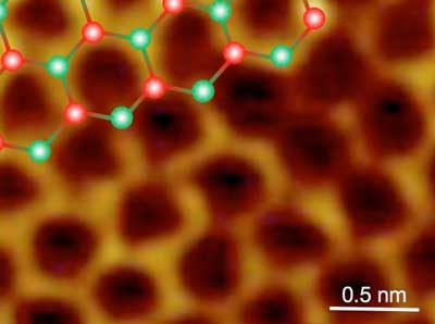
Stanene
High-resolution STM image of stanene prepared on a Ag2Sn surface alloy. The honeycomb stanene structure model is superimposed. (Image: Junji Yuhara)
Just as graphene differs from ordinary graphite, so does stanene behave very differently to humble tin in bulk form. Because of relatively strong spin-orbit interactions for electrons in heavy elements, single-layer tin is predicted to be a „topological insulator,” also known as a quantum spin Hall (QSH) insulator. Materials in this remarkable class are electrically insulating in their interiors, but have highly conductive surfaces/edges. This, in theory, makes a single-layered topological insulator an ideal wiring material for nanoelectronics. Moreover, the highly conductive channels at the edge of these materials can carry special chiral currents with spins locked with transport directions, which makes them also very appealing for spintronics applications.
In previous studies, where stanene was grown on substrates of bismuth telluride or antimony, the tin layers turned out to be highly buckled and relatively inhomogeneous. The Nagoya team instead chose silver (Ag) as their host – specifically, the Ag(111) crystal facet, whose lattice constant is slightly larger than that of the freestanding stanene, leading to the formation of flattened tin monolayer in a large area, one step closer to the scalable industrial applications.
Individual tin atoms were slowly deposited onto silver, known as epitaxial growth. Crucially, the stanene layer did not form directly on top of the silver surface. Instead, as shown by core-level spectroscopy, the first step was the formation of a surface alloy (Ag2Sn) between the two species. Then, another round of tin deposition produced a layer of pure, highly crystalline stanene atop the alloy. Tunneling microscopy shows striking images of a honeycomb lattice of tin atoms, illustrating the hexagonal structure of stanene.
The alloy guaranteed the flatness of the tin layer, as confirmed by density-functional theory calculations. Junji Yuhara, lead author of an article by the team published in 2D Materials („Large area planar stanene epitaxially grown on Ag(1 1 1)”), explains: „Stanene follows the crystalline periodicity of the Ag2Sn surface alloy. Therefore, instead of buckling as it would in isolation, the stanene layer flattens out – at the cost of a slight strain – to maximize contact with the alloy beneath.” This mutual stabilization between stanene and host not only keeps the stanene layers impeccably flat, but lets them grow to impressive sizes of around 5,000 square nanometers.
Planar stanene has exciting prospects in electronics and computing. „The QSH effect is rather delicate, and most topological insulators only show it at low temperatures”, according to project team leader Guy Le Lay at Aix-Marseille University. „However, stanene is predicted to adopt a QSH state even at room temperature and above, especially when functionalized with other elements. In the future, we hope to see stanene partnered up with silicene in computer circuitry. That combination could drastically speed up computational efficiency, even compared with the current cutting-edge technology.”
Source: Nagoya University