O stare cuantică rară realizată într-un material nou(A rare quantum state realized in a new material)

O stare cuantică exotică numită Dirac semimetal a fost realizat într – un roman Sr material magnetic 1-y Mn 1-z Sb 2 ( Nature Materials , „A magnetic topologic semimetal Sr 1-y Mn 1 z Sb 2 (y , z <0,1) " ). Acest material prezintă o combinație neobișnuită de două comportamente electronice distincte. Un comportament este persistența unei stări asemănătoare cu un magnet de bar cu rotiri care sunt paralele între ele. Celălalt se referă la electroni cu o masă efectivă aproape de zero care se deplasează aproape de viteza luminii.

Posted: Jan 10, 2018

A rare quantum state realized in a new material

(Nanowerk News) An exotic quantum state called a Dirac semimetal was realized in a novel magnetic material Sr1-yMn1-zSb2 (Nature Materials, „A magnetic topological semimetal Sr1-yMn1-zSb2 (y, z < 0.1)”). This material features an unusual combination of two distinct electronic behaviors.

One behavior is the persistence of a state similar to a bar magnet with spins that are parallel to each other. The other relates to electrons with an effective mass near zero that travel close to the speed of light.
The artwork depicts the magnetic and electronic states of a magnetic topological semimetal
The artwork depicts the magnetic and electronic states of the newly discovered magnetic topological semimetal (Sr1-yMn1-zSb2); its unusual and robust electronic behavior enables the flow of electrical current with little resistance. The violet spheres are strontium (Sr), blue is antimony (Sb), and purple is manganese (Mn). Arrows represent the alignment of magnetic moments. The two gold cones touching at a point (called Dirac point) represent the energy and momentum states of conducting electrons. (Image: Oak Ridge National Laboratory)
The Dirac semimetal belongs to a class of materials called topological semimetals. These materials offer great promise. They could be the basis for ultra-powerful computers. Essentially, the semimetal could create a new paradigm for highly efficient and robust computational platforms. Semimetals could let such computers and other quantum devices work in warmer settings, climbing further from absolute zero.
A 3-D analog of graphene (a 2-D material) is a Dirac semimetal. Dirac semimetals have exceedingly high charge carrier mobility, creating little to no resistance to current flow, and large magnetoresistance that could be used for high-density, low-power data storage.
A team led by Tulane University, Louisiana Consortium for Neutron Scattering at Louisiana State University, and others discovered a new magnetic semimetal Sr1-yMn1-zSb2 (y, z<0.1) with nearly massless quantum particles (electrons in this case) that follow the rules of relativistic quantum mechanics.
Neutron scattering experiments revealed an unusual combination of ferromagnetic and antiferromagnetic states in the material that vary as a function of temperature. In general, materials exhibit either ferromagnetism or antiferromagnetism, not both in the same material at a given condition.
The observed persistence of a ferromagnetic component in the antiferromagnetic state at low temperatures is the signature for the breaking of the time-reversal symmetry (that is, running backward does not return to its starting conditions).
The combination of unusual electronic behaviors in this new material offers a rare opportunity to investigate the interplay between relativistic quantum states and spontaneous breaking of symmetry associated with time. These materials offer great promise for highly efficient quantum devices and quantum computers.
Source: U.S. Department of Energy, Office of Science

Camerele solare lavabile(Washable solar cells)

„fotovoltaice organice elastice acoperite cu elastomer rezistent la apă și etanșă pentru aplicații electronice lavabile” ). Noile celule fotovoltaice organice, ultrathine pot fi întinse la jumătatea lungimii lor și pot rezista la 20 de cicluri de spălare simulate.
Posibilitățile sunt tantalizante. Aceste proprietăți înseamnă că celulele ar putea fi încorporate, de exemplu, în dispozitivele textile și în dispozitivele Internet-of-Things (dispozitive în rețea care pot „vorbi” unul cu celălalt) pentru a crea îmbrăcăminte generatoare de energie electrică; power monitors personal health; și reîncărcați dispozitive mobile în mișcare.

Posted: Dec 22, 2017

Washable solar cells

(Nanowerk News) Hard, flat solar panels are hardly something most people want to wear against their skin. However, flexible, washable solar cells are on the horizon thanks to a recent breakthrough by a team at RIKEN led by Takao Someya (Nature Energy, „Stretchable and waterproof elastomer-coated organic photovoltaics for washable electronic textile applications”). The new organic, ultrathin photovoltaic cells can be stretched by half their length and withstand 20 simulated washing cycles.

The possibilities are tantalizing. These properties mean the cells could, for example, be incorporated into textiles and Internet-of-Things devices (networked devices that can ‘talk’ to each other) to create electricity-generating clothing; power personal health monitors; and recharge mobile devices on the go.
A photograph showing the ultrathin organic solar cell being washed and stretched
A photograph showing the ultrathin organic solar cell being washed and stretched. (Image: RIKEN)

An accordion in an elastomer sandwich

This is the first time that a single solar cell has combined a high energy efficiency, stretchabil­ity, and stability in air and water, explains lead researcher Kenjiro Fukuda from the Thin-Film Device Laboratory (Chief Scientist Laboratory) and the RIKEN Center for Emergent Matter Science (CEMS).
The work began, he says, when Kazuo Takimiya’s group at CEMS developed the solar cell’s ultrathin organic active layer, an organic photovoltaic (OPV). The layer converts sunlight into electricity at an efficiency of nearly 8 per cent, while also being very stable in air and water. Thicker OPVs can claim a peak conversion of 10 per cent—but for a photovoltaic material that is only 1 micrometer thick, 8 per cent is very high. And since the active material is very thin and based on an organic material, it can flex without breaking.
But the first solar cells produced with this active layer were not stretchable and were easily scratched. Fukuda’s group solved these issues by placing stretched rubber-like elastomer films over the outside. “First, we pre-stretch the elastomer and fix the ultrathin solar cells gently,” says Fukuda. “Next, the second elastomer is pre-stretched and attached, and we achieve this kind of sandwich structure.” When the elastomer films were allowed to relax, the embedded solar cell folded itself into an accordion-like structure with troughs and peaks.
This folded structure gives the cell its stretchability—when it is pulled, the folds flatten out, meaning the device can be extended up to half its length without damage.
The elastomer films also somewhat water­proofed the cells making them washable— something that the researchers tested by subjecting the cells to 20 cycles of mechanical compression while exposing them to water for one hour and 40 minutes. The cell’s efficiency dropped by only 20 per cent after this process.

Stretchy batteries needed

The hope is that these solar cells could power electronic devices such as sensors to measure a wearer’s heart rate, body temperature, blood pressure and other important medical parame­ters. They could also allow doctors to more easily monitor an out-patient’s condition as well as enable athletes to continually measure their per­formance. “Recently, smart sensors that monitor the heartbeat, pressure or electrodermal activity, have been attracting attention,” says Fukuda. “So there are now a lot of textiles with sensors embedded. By combining these technologies with our solar cells, we could achieve some very smart sensor clothes systems.”
Making a solar cell stretchable
Making a solar cell stretchable. (Image: RIKEN)
In the future, if sufficiently high voltages and currents can be realized, solar cells in clothing could also be used to recharge mobile devices and may even be able to supply household electricity, meaning things like OPV awnings could be used in, for example, developing regions.
And if the solar cells could be combined with thin, lightweight batteries, their usefulness could be enhanced even further. “We need a very thin or stretchable battery system, but this very difficult to realize,” says Fukuda. “Batteries need some thickness to store a lot of power.” But he adds: “If we can find a suitable collaborator, we could realize good synergy between our team and a battery research group.”

Commercializing the technology

Currently, OPV models cannot compete against traditional inorganic solar cells for longevity and therefore price. Rooftop models target lifetimes of 20 years, while organic photovoltaic cells are targeting lifetimes of less than 10 years for glass-based products and less than five years for flexible products. German researchers Ning Li and Christoph J. Brabec noted this in a commen­tary piece on RIKEN’s OPVs for Nature Energy.
But Brabec, who is from the Department of Material Science at Germany’s Friedrich-Alex­ander University Erlangen-Nürnberg, says: “We got excited about [Someya and Fukuda’s] work as it fits excellently into what we suggest as the roadmap for OPVs….[We] believe that OPVs should concentrate on integrated applications.”
“Integration into bags, glasses, etc. has been around for quite some time, but integration into textiles hasn’t been possible because OPVs couldn’t be washed.”
Fukuda says that real-world practical applications are probably three to five years down the track, but already there has been interest from companies in commercializing the technology.
The two main hurdles that will need to be overcome are the cost and size of the solar cells. The cells are currently limited to 10 centimeters by 10 centimeters and are fairly expensive to fabricate. But this is mostly down to the cost of the active layer, says Fukuda. The film coating, he says, is actually very thin and will ultimately reduce costs. “If companies commercialize this technology, they could develop a way to mass-produce the active layer material and reduce the cost.”
“Many companies are interested in our technology and have contacted us recently,” he says. “Collaborating with a company will accelerate commercialization.”
Fukuda and his team are currently working on improving the cells’ stability in air and stretchability.
Source: RIKEN

Un act de echilibrare catalitică(A catalytic balancing act)

Creând mai întâi un aliaj de două dintre cele mai dense elemente naturale și apoi eliminând unul, oamenii de știință au remodelat structura materialului rămas astfel încât să echilibreze mai bine trei factori importanți pentru reacțiile chimice: activitate, stabilitate și conductivitate.
„Găsirea unui material care să funcționeze bine pentru conversia sau stocarea energiei este ca și cum ai crea o căsnicie fericită”, a declarat Nenad Markovic, un cercetător în domeniul materialelor Argonne și autor al studiului. „În cazul nostru, am constatat că un parteneriat dinamic între două materiale diferite ne-a ajutat să integrăm preocupările concurente”.În condiții de funcționare, catalizatorul poros formează de fapt o carcasă unică de oxid de iridiu mai puțin conductiv în jurul interiorului metalic de iridiu foarte conductiv. În acest fel, electronii se pot mișca ușor prin cea mai mare parte a catalizatorului pentru a ajunge la suprafață, unde molecula de apă așteaptă pe electroni să inițieze reacția de divizare a apei.

Posted: Dec 22, 2017

A catalytic balancing act

(Nanowerk News) Balance forms the foundation for a happy life or a healthy diet. For scientists working to design new catalysts to create renewable energy, balancing different materials and their properties is equally important. (Catalysts help accelerate chemical reactions.)

In a new study (Nature Communications, „Balancing activity, stability and conductivity of nanoporous core-shell iridium/iridium oxide oxygen evolution catalysts”), researchers from the U.S. Department of Energy’s (DOE) Argonne National Laboratory, Johns Hopkins University, Drexel University and several universities in South Korea used a new and counterintuitive approach to create a better catalyst that supports one of the reactions involved in splitting water into hydrogen and oxygen. Scientists plan to use the generated hydrogen as a clean fuel.
By first creating an alloy of two of the densest naturally occurring elements and then removing one, the scientists reshaped the remaining material’s structure so that it better balanced three factors important for chemical reactions: activity, stability and conductivity.
“Finding a material that works well for energy conversion or storage is like creating a happy marriage,” said Nenad Markovic, an Argonne materials scientist and author of the study. “In our case, we found that a dynamic partnership between two different materials helped us integrate competing concerns.”
Scientists searching for new catalysts have scoured the periodic table to find the right elements or combinations of elements to maximize a catalyst’s activity in water-splitting reactions, as well as the durability of the active sites on its surface. Finding materials that are both stable and active, however, has been a challenge.
“More active catalysts tend to be less stable,” Markovic said. “Those that seem to work twice as well usually work only half as long. It is becoming obvious that designing active catalysts is not enough — we need to have not only active, but also stable, materials.”
For the new catalyst, Markovic and his colleagues turned to iridium, a metal most commonly associated with meteorites. As a thin film, iridium is catalytically active, but as it reacts over time with an electrolyte environment, iridium atoms become oxidized. During this process, some of them leave the catalyst’s surface through corrosion, increasingly impairing its performance.
The research team worked to prevent the oxidation by reorganizing the iridium’s structure. To help stabilize and activate iridium, they alloyed it with its neighbor on the periodic table, osmium.
Unlike iridium, osmium is neither catalytically active nor stable, but it did offer a key benefit. After alloying the osmium and iridium together, the researchers then de-alloyed the two metals, leaving behind only a reconfigured structure of three-dimensional iridium nanopores.
“Without the osmium, the iridium would never achieve this state,” Markovic said. “We needed to introduce and then remove the osmium to get a form of iridium that was both active and stable.”
Markovic said each nanopore’s enhanced catalytic stability is due to the small volume of electrolyte within a pore becoming quickly saturated with iridium ions so that surface atoms stop dissolving, in much the same way that it is easier to saturate a teacup of water with sugar than a 10-gallon jug.
While the nanopore’s structure addressed the need for a stable, active catalyst, it was another facet of the iridium’s reconfiguration that helped boost the material’s electron conductivity. Under operational conditions, the porous catalyst actually forms a unique shell of less-conductive iridium oxide around its highly conductive iridium metal interior. This way, electrons can move easily through most of the catalyst to reach the surface, where the water molecule waits on electrons to initiate the water-splitting reaction.
“Essentially, we’re trying to find a way to send electrons through on the ‘expressway,’ rather than making them take the side roads,” Markovic said. “This core-shell configuration [of the nanoporous material] allows us to do that.”
Source: Argonne National Laboratory

Ajungem sub pielea grafitului(Getting under graphite’s skin)

Oamenii de stiinta de la Laboratorul Ames al Departamentului de Energie din SUA au descoperit un nou proces de imbracare a metalelor sub un singur strat de grafit care pot conduce la proprietati noi si mai bine controlate pentru aceste tipuri de materiale

Posted: Dec 18, 2017

Getting under graphite’s skin

(Nanowerk News) Scientists at the U.S. Department of Energy’s Ames Laboratory have discovered a new process to sheathe metal under a single layer of graphite which may lead to new and better-controlled properties for these types of materials (Carbon, „Defect-mediated, thermally-activated encapsulation of metals at the surface of graphite”).

A 'mesa' of dysprosium, draped with a single layer of graphene
A „mesa” of dysprosium, draped with a single layer of graphene. Research from Ames Laboratory suggests that this method will work with a wide variety of metal and graphite combinations, opening up the possibility of diverse applications including quantum computing, solar cells, catalysis, and sensing. (Image: Ames Laboratory)
Graphene—two-dimensional graphite—was first produced in 2004, and because electrons move rapidly along its surface, holds great promise as a useful material in applications as diverse as quantum computing, solar cells, catalysis, and sensing. In order for graphene to live up to that potential, fundamental discovery science at Ames Laboratory is working to master its assembly in combination with other materials—a tricky, delicate process performed in ultra-high vacuum lab environments at the atomic scale.
The researchers encapsulated dysprosium, a magnetic rare-earth metal, by bombarding the top layer of bulk graphite with ions to create defects on its surface, followed by high-temperature deposition of the metal. It resulted in “mesas” or islands of dysprosium underneath a single layer of graphene. The formations are significantly different than anything the Laboratory’s two-dimensional materials experts have ever seen.
“It’s well-known that certain metals can be embedded between bulk graphite layers,” said Research Assistant Ann Lii-Rosales. “But these mesas form at the top graphite surface only, and they are pure metal composed of multilayers, which is a first. The combined properties of the metal plus graphene may be very different than other, previously produced materials. That’s something we’re exploring now.”
The researchers were also able to achieve the same mesa-like formations with two transition metals, ruthenium and copper.
“That suggests we have a very adaptable recipe for producing this kind of surface material, which makes its discovery very exciting in terms of potential applications,” said Pat Thiel, an Ames Laboratory scientist and Distinguished Professor of Chemistry and Materials Science and Engineering at Iowa State University. “If we can control the process so that we can deliberately pattern the formation of these little metal slabs, perhaps we can harness and control their magnetic and electronic properties.”
Source: Ames Laboratory

Înregistrați fotoconductivitatea ridicată pentru noul material cadru metalic-organic(Record high photoconductivity for new metal-organic framework material)

MOF sunt materiale compuse care sunt fabricate din ioni și liganzi pentru a face structuri tridimensionale. MOF-urile sunt în mod obișnuit folosite pentru a stoca gaze și pentru a separa și purifica substanțele chimice, dar oamenii de știință speră că noua lor descoperire ar putea duce la folosirea MOF pentru a face materiale fotoactive, cum ar fi celulele solare.
Profesorul Ravi Silva, directorul Institutului de Tehnologie Advance, a declarat: „Cadrele organice din metal au câștigat un interes extraordinar de târziu pentru potențialul lor de a fi utilizate pentru stocarea gazului, pentru detectarea și cataliza – dar este clar că acestea ar putea fi utilizate pentru mult mai mult.

Posted: Dec 15, 2017

Record high photoconductivity for new metal-organic framework material

(Nanowerk News) An international team of scientists, from the University of Surrey, University of São Paulo (Brazil), the University of Warwick and the University of Grenoble-Alpes (France), has created a new metal-organic framework (MOF) that has shown record-high photo-conductivity levels for a material of its type.

A representation of MOF-CoNDI-py-2 crystal structure including its unit cell obtained by single-crystal XRD
A representation of MOF-CoNDI-py-2 crystal structure including its unit cell obtained by single-crystal XRD. Pink = cobalt, grey = carbon, white = hydrogen, blue = nitrogen and red = oxygen. The unit cell belongs to a C2/c monoclinic space group, water was modelled at 1/4 occupancy and its hydrogens are not shown for clarity. The structure shows the NDI-py molecules oriented in a layered fashion. The distances between NDI-py entities are 9.43 Å along the c-axis, 9.57 Å along the b-axis and 11.10 Å through the metal cluster. (© NPG)
The team published its findings in Nature Communications („Electrical conduction modulated by light in a cobalt and naphthalene diimide metal-organic framework”) where it reported that its MOF had a responsivity rate of 2.5 x 10⁵ amperes per watt. The team’s MOF was made by using cobalt (II) ions and naphthalene diimides and acid ligands.
MOFs are compound materials that are made of ions and ligands to make 3 dimensional structures. MOFs are typically used to store gas and to separate and purify chemicals, but the scientists hope that their new discovery could lead to MOFs being used to make photoactive materials such as solar cells.
Professor Ravi Silva, Director of the Advance Technology Institute, said: “Metal Organic Frameworks have been gaining a tremendous amount of interest of late for their potential to be used for gas storage, sensing and catalysis – but it is clear that they could be used for so much more.
“This is a great example of how collaborating on an international scale can result in truly exciting discoveries that have the potential to change the direction of a number of industries.”
Source: University of Surrey

Nanostructurile controleaza transferul de caldura: Cercetatorii demonstreaza noile concepte pentru managementul caldurii(Nanostructures control heat transfer: Researchers demonstrate new concepts for heat management)

demonstrează că este posibil ca, în principiu, să se regleze conductivitatea termică a materialelor nanostructurate cu un grad ridicat de precizie, însă materialele în curs de dezvoltare care permit controlul precis al transferului termic sunt doar începutul. au dezvaluit concepte interesante pentru construirea de materiale izolante mai eficiente din punct de vedere energetic

Posted: Dec 15, 2017

Nanostructures control heat transfer: Researchers demonstrate new concepts for heat management

(Nanowerk News) For the first time, Prof. Dr. Markus Retsch and his research group at the University of Bayreuth have succeeded in precisely controlling temperature-dependent thermal conductivity with the help of polymer materials. These advanced functional materials – initially produced for laboratory experiments – have now been presented in the journal Science Advances(„Tailor-made temperature-dependent thermal conductivity via interparticle constriction”). The findings are of great relevance to the development of new concepts of thermal insulation.

An electron microscope image displaying the regular nanostructure of a photonic crystal
An electron microscope image displaying the regular nanostructure of a photonic crystal. Scale bar: 5 micrometres. (Image: Markus Retsch)

From butterfly wings to new functional materials

The polymer materials that allow thermal conductivity to be controlled are photonic crystals. They often give butterflies, beetles, and other insects dazzling colours and have mainly been investigated due to their optical effects. Prof. Dr. Markus Retsch, Lichtenberg Junior Professor of Polymer Systems, and his doctoral student Fabian Nutz (M.Sc.) have developed four different methods to control temperature-dependent heat transfer in such photonic crystals.
These methods exploit the fact that polymer nanomaterials become more heat-permeable once they lose their nanostructure by crossing a certain temperature threshold. That is when the thermal conductivity of the photonic crystals skyrockets to a level that is two or three times as high as it was before. On this basis, clearly defined effects on thermal transfer can be achieved via changes in the nanostructure of the crystals.

Film formation increases thermal conductivity

The research of the scientists in Bayreuth has shown that the temperature at which thermal conductivity jumps to a higher level depends crucially on the composition of the nanoparticles that make up the photonic crystals. This temperature can be precisely adjusted by incorporating a plasticizer into the polymer structure. Whether thermal conductivity changes within a wide or narrow temperature range when the temperature rises can also be precisely controlled: doing so only requires nanoparticles which are similar in size but which differ with regard to plasticizer content to be equally mixed. This leads to a gradual loss of the nanostructure across a wide temperature range. Consequently, the increase in thermal conductivity also spans a larger temperature range.
In addition, by using a layered structure, the researchers also managed to transform the continuous increase into a multi-level increase in conductivity. By adjusting the thickness of individual crystal layers, one can also precisely influence the conductivity level that is reached at the respective level.

Potential for energy technology and thermal management

„These research findings demonstrate that it is possible in principle to regulate thermal conductivity in nanostructured materials with a high degree of precision. However, developing materials that enable thermal transfer to be precisely controlled is only the beginning. Our findings to date are very encouraging and have revealed interesting concepts for constructing more energy efficient insulation materials. In the long term, these concepts could be valuable for the development of thermal transistors or diodes,” Prof. Retsch explained.
He did, however, point to one obstacle that must still be overcome: the increase in thermal conductivity – as regulated in the four methods developed by the team – is irreversible. This means that the conductivity remains at the level that is reached even when the temperature sinks again. „Constructing nanosystems that enable thermal transfer to be reversibly controlled is a difficult yet exciting and central task for further research in this field,” said Prof. Retsch.
Source: University of Bayreuth

Primul cristal lichid cuantic tridimensional(The first three-dimensional quantum liquid crystal)

Acest material trece printr-o tranziție de fază structurală la o temperatură critică de tranziție (200 Kelvin), unde structura cristalină se schimbă de la cubică la tetragonală. Întrebarea este: ce conduce această tranziție și cum ar putea fi legată de structura și interacțiunile electronice?poate fi un precursor al superconductivității topologice mult timp căutate.

Posted: Dec 14, 2017

The first three-dimensional quantum liquid crystal

(Nanowerk News) Scientists discovered an entirely new class of novel electronic structures. They discovered a liquid crystal-like quantum phase of matter in a 3-D material. The onset of this phase at the transition temperature is very subtle, yet, like a rudder steering a large ship, it drives a much larger effect—a structural phase transition (Science, „A parity-breaking electronic nematic phase transition in the spin-orbit coupled metal Cd2Re2O7„).

The patterns show reflected laser light at twice the initial laser frequency observed when illuminating the metal Cd2Re2O7
Using optical second harmonic generation spectroscopy, scientists discovered a new state of matter. The patterns show reflected laser light at twice the initial laser frequency observed when illuminating the metal Cd2Re2O7. The patterns were collected from Cd2Re2O7 crystals at temperatures that were above (left) and below (right) a structural phase transition temperature (Tc), which occurs at 200 Kelvin. Scientist have concluded that the low-temperature pattern arises from a 3-D quantum liquid crystal. (Image: David Hsieh, California Institute of Technology)
This discovery represents a quantum analog of classical 3-D liquid crystals. These new structures are among those that are observed as a consequence of competing interactions in 3-D metals. The competitions lead to phenomena such as ferromagnetism, which leads to the formation of permanent magnets, and superconductivity that allows electrical current to flow with zero resistance. This new class of materials may have applications in ultrafast computers.
The spatial arrangement of atoms and electrons in a material is often characterized by its symmetry, which has an important role in determining the electronic properties of the material. In materials where conduction electrons are strongly interacting, it is possible for electronic configurations to exhibit a different symmetry than the underlying crystal lattice.
The material Cd2Re2O7 is a poor metal characterized by strong electron-electron interactions and coupling between the electron’s spin orientation and orbital motion in atoms.
This material undergoes a structural phase transition at a critical transition temperature (200 Kelvin) where the crystal structure changes from cubic to tetragonal. The question is, what drives this transition and how might it be related to the electronic structure and interactions?
Researchers obtained patterns of reflected light by illuminating a Cd2Re2O7 crystal with a laser and then collecting the reflected light that has been converted to twice the frequency of the initial laser. Changes in the pattern led scientists to conclude that the temperature-dependent phase transition is driven by an unusual electronic liquid crystalline (nematic) order that spontaneously breaks certain types of symmetry (rotational and inversion) in the crystal.
Scientists also demonstrated that the structural transformation follows, or is subject to, the electronic transition rather than the more commonly observed process where a structural transformation changes the electronics. Such nematic order was theoretically predicted to appear in correlated metals with strong spin-orbit coupling and may be a precursor to long-sought topological superconductivity.
Source: Department of Energy, Office of Science

Modele lungi, formate în apă și magneți(Long-ranged patterns formed in water and magnets)

Știința și tehnologia modernă au dezvoltat noi tipuri de materie cu proprietăți nefamiliare și ocazional utile. Materialele cunoscute sub denumirea de „gheață de spin” oferă un tip complet nou de magnetism, incluzând curenți de încărcături magnetice sau „monopoluri” și, prin urmare, un echivalent magnetic de energie electrică – „magnetricitatea”.

Posted: Dec 14, 2017

Long-ranged patterns formed in water and magnets

(Nanowerk News) Modern science and technology has developed new types of matter with unfamiliar and occasionally useful properties. The materials known as “spin ice” offer a completely new type of magnetism, including currents of magnetic charges or “monopoles” and hence a magnetic equivalent of electricity – “magnetricity”.

The “spins” that form “spin ice” are like atom-sized compass-needles that may be represented as arrows. The “ice” in “spin ice” refers to a deep theoretical connection with the properties of familiar ice, or solid water, H2O. If one were to place a hydrogen atom (H) on the end of every spin arrow in ice, then one would generate a pattern of H-atoms in water ice.
New research (Nature Communications, „Harmonic phase in polar liquids and spin ice”) at the London Centre for Nanotechnology and Department of Physics & Astronomy, UCL, has revealed a further deep connection between the properties of spin ice ice and those of water in its more important liquid state, so crucial to life on earth.
How a central molecule in a polar liquid such as water, or a spin in spin ice, orients the other molecules or spins around it
How a central molecule in a polar liquid such as water, or a spin in spin ice, orients the other molecules or spins around it. (Image: LCN)
Water is a so-called “polar liquid” – each water molecule is an electrical dipole, with a positive charge at one end and a negative charge at the other. This is revealed, for example, when a stream of tap water is deflected by a pen that has been charged with static electricity. However, the dipoles in polar liquids like water do not point in random directions but in fact form subtle patterns over extremely long distances.
The new research has shown that the same long-ranged patterns that form in polar liquids are also formed by the spins in spin ice. In both cases the patterns are described mathematically by so-called “harmonic” functions. Hence polar liquids, including water, and spin ice have been collectively referred to as “harmonic” phases. Here a “phase” is a term used to describe different portions of matter that share the same property.
The author of the work, LCN Professor Steve Bramwell, comments “it’s remarkable to discover that the same long-ranged patterns form in an exotic magnet—spin ice—and in polar liquids such as water: this should help us to predict new properties of both types of material.”
The patterns formed by the molecular dipoles in polar liquids and the spins in spin ice can be visualised if one imagines oneself “sitting” on a particular dipole or spin. Then the pattern looks like the familiar pattern of iron filings that forms around a bar magnet. As the central dipole or spin moves, then this pattern moves with it.
Source: London Centre for Nanotechnology

Vehiculele ar putea obține „nervii” acel prejudiciu sens cu noi cercetări(Vehicles could get ‘nerves’ that sense damage with new research)

Elicopterele, rezervoarele și alte vehicule ar putea fi făcute într-o bună zi dintr-un „material inteligent” care să simtă daune, similar cu modul în care nervii spun organismului că a fost rănit, Ideea este că materialul sensibil din punct de vedere magnetic ar fi încorporat în materialul inteligent de pe întregul vehicul și va acționa ca un senzor care spune: „Avem daune aici”

Posted: Dec 13, 2017

Vehicles could get ‘nerves’ that sense damage with new research

(Nanowerk News) Helicopters, tanks and other vehicles could someday be made of „smart material” that senses damage, similar to how nerves tell the body it has been injured, with the help of new research based at Clemson University and funded by the U.S. Army Research Laboratory.

The idea is that magnetically sensitive material would be embedded within the smart material throughout the vehicle and act as a sensor that says, „Ouch! We have damage here,” said Oliver Myers, an associate professor of mechanical engineering.
Just as pain is relayed to the brain, the damage report would go to a computer and help determine whether a vehicle should keep going or return to the depot.
„In the field, we need that self-diagnostic capability,” Myers said. „Lieutenant Data in ‘Star Trek’ always says, ‘I’m performing to specified parameters.’ We want to make sure our platforms are performing to those specified parameters at a minimum.”
Myers is receiving $993,492 from the U.S. Army Research Laboratory to lead the project.
Oliver Myers (right) and mechanical engineering master's student Brandon Williams
Oliver Myers (right) and mechanical engineering master’s student Brandon Williams work with some of the smart material they are developing at Clemson University. (Image: Clemson University)
The research could help the Army save money on rotorcraft maintenance, said Asha Hall, the lead co-principal investigator and Prognostics and Diagnostics Acting Team Lead within the Mechanics Division of the Vehicle Technology Directorate at the U.S. Army Research Laboratory.
As a safety measure, the Army replaces some parts based on how long they have been in service, whether they appear damaged or not, she said. Embedded sensors could make it possible for parts to remain in service longer, based on their condition, Hall said.
„We’re trying to extend that maintenance-free operating period,” she said. „The big, big impact is to reduce sustainment costs for the Army.”
The research builds on the fast-growing field of composite materials, which are used in a variety of products from cars to airplanes. Composite materials often look and feel like plastic but are lighter and stronger than metals, including steel.
The team is sandwiching „magnetostrictive” material between multiple layers of composite materials, creating a laminate. The magnetostrictive material responds to a magnetic field or a change in stress, allowing it to act as the nerve that senses the damage.
„The composite laminate effectively becomes a smart structure,” Myers said.
The types of damage it could detect include impacts, cracking and unusual loading, he said.
Part of what makes the team’s approach unique is that the magnetostrictive material that senses the damage is embedded in the structure itself during the fabrication process, rather than attaching sensors after the structure is already built. Those external sensors often require additional equipment, Myers said.
The magnetostrictive material requires no power, is lightweight and operates in harsh environments, he said.
Richard Figliola, acting chair of the Department of Mechanical Engineering, said that Myers was well qualified to lead the research.
„Dr. Myers has deep experience in smart materials and smart structure mechanics of systems ranging from nano- to macro-scales sizes,” Figliola said. „He has written journal articles and attended conferences to develop relationships with his collaborators. The award is well deserved.”
Myers said the research was inspired by his master’s work in the Mechanical Engineering Department at the University of Maryland, Baltimore County, where he studied under the Meyerhoff Scholarship Program. That’s when he began playing with the idea of embedding materials in composite structures to see if damage could be detected.
At the time, he did it on a small scale.
Deployment to the field could be 10-20 years away, but Myers aims to move the research in that direction.
The central question Myers is asking is how the team can create a „robust sensing operation” using the embedded magnetostrictive material. Robust would mean it is observable, repeatable, measurable and sustainable, he said.
„We want this to not only be a benchtop experiment, but we want to be able to put it on larger structures and larger systems so that once we go from the benchtop coupon level we go to a full-size system and have it function as an NDE, or nondestructive evaluation, structural health-monitoring platform,” he said.
Anand Gramopadhye, dean of the College of Engineering, Computing and Applied Sciences, congratulated Myers on the award.
„His cutting-edge, innovative research could produce discoveries that have a significant impact on operational capabilities and technologies for the Army,” Gramopadhye said. „The amount of the award is a testament to his hard work, the creativity of his approach and his leadership in creating smart materials.”
Source: Clemson University

Oamenii de stiinta au sugerat o noua tehnologie pentru crearea de micro-structuri magnet(Scientists suggested a new technology for creating magnet micro-structures)

Echipa a creat filme groase de sute până la zeci de nanometri. Filmele dezvoltate sunt formate din siliciuri de fier sintetizate pe un substrat de siliciu. Silicidele de fier sunt compuși ai fierului și siliciului care de obicei au proprietăți feromagnetice atunci când sunt supuși anumitor temperaturi.

Posted: Dec 12, 2017

Scientists suggested a new technology for creating magnet micro-structures

(Nanowerk News) A team of scientists from Krasnoyarsk Scientific Center (Siberian Department of Russian Academy of Sciences) and Siberian Federal University synthesized thin crystal ferromagnetic films and developed a technology for their shaping. Processed films can be used in electronic and spintronic chips. The results of the study were published in Thin Solid Films.

The team created films that are hundreds to dozens nanometers thick. The developed films are formed of iron silicides synthesized on a silicon substrate. Iron silicides are compounds of iron and silicon that usually have ferromagnetic properties when subject to certain temperatures. There are also non-magnetic iron silicides with unique optic characteristics that may be put to practical use.
crystal thin film
This is the configuration of a thin crystal film. (Image: Anton Tarasov)
Films like this are used as active parts in optic and photonic devices, as well as in integral electronic and spintronic chips. Thin ferromagnetic films open a lot of prospects for spintronics (an area of science that provides for the creation of information storage and processing devices). Devices like this consume less electrical energy and have higher operating speed compared to traditional electronic ones.
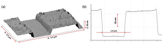
However, to develop such devices scientists need films to be specifically shaped. It means that a template has to be applied to synthesized films, and they have to be cut according to it. To do so, scientists use etching. It can be either wet (chemical) or dry (plasma, reactive-ion, or just ion). In the course of wet etching a film is placed in liquid – an etching agent that dissolves the rest of it. Before that scientists cover the films with „masks” using photolitography to set out required configuration. Such a mask protects the desired part of the film from solving. In dry etching the same result is achieved using a gas that destroys the material physically or chemically.
„We’ve broadened the application of this approach, extended it to new iron-silicon alloys, and showed that it works. We’ve also determined the speed of etching and developed a micro-device. The same methods may be used for the production of different structures in electronics, photonics, and other applications,” said Anton Tarasov, a co-author of the article, candidate of physical and mathematical sciences, a scientific associate of Kirensky Institute of Physics (FRC KSC of SD RAS), and senior tutor at Siberian Federal University.
Scientists point out that a big advantage of the new films is not only their electronic and magnetic properties, but compatibility with the most popular technological semiconductors. It means, these films may be grown on bases made of silicon, germanium, and gallium arsenide. This will help the team obtain high-quality thin films with specific shapes and geometry in a simpler and more affordable way. Moreover, the obtained results increase the selection of materials that scientists may use to develop different devices.
„Using this technology, one can create spintronic or photonic devices, because iron silicides have properties applicable in these areas of science. Right now we are growing new films and studying the effects that depend on their topology,” concluded the scientist.
The team worked in collaboration with scientists from Siberian State Aerospace University and Lomonosov Moscow State University. The research was supported with grants from Russian Foundation for Basic Research and Krasnoyarsk Regional Science Foundation, as well as with the grant of the President of the Russian Federation for the support of leading scientific establishments.
Source: Siberian Federal University

Inginerii creează grafen în mod artificial într-o structură semiconductoră nanofabricată(Engineers create artificial graphene in a nanofabricated semiconductor structure)

Acest grafen artificial are mai multe avantaje față de grafenul natural: de exemplu, cercetătorii pot proiecta variații în grilaj de fagure pentru a modula comportamentul electronic. Și deoarece distanța dintre punctele cuantice este mult mai mare decât distanța inter-atomică în grafenul natural, cercetătorii pot observa fenomene cuantice chiar mai exotice prin aplicarea unui câmp magnetic.
Descoperirea de noi materiale cu dimensiuni reduse, cum ar fi grafenul și alte straturi superficiale, straturi van der Waals care prezintă fenomene fizice noi, care au fost anterior inaccesibile, au pus bazele acestui studiu.

Posted: Dec 12, 2017

Engineers create artificial graphene in a nanofabricated semiconductor structure

(Nanowerk News) Researchers at Columbia Engineering, experts at manipulating matter at the nanoscale, have made an important breakthrough in physics and materials science, recently reported in Nature Nanotechnology („Observation of Dirac Bands in Artificial Graphene in Small Period Nano-patterned GaAs Quantum Wells”). Working with colleagues from Princeton and Purdue Universities and Istituto Italiano di Tecnologia, the team has engineered “artificial graphene” by recreating, for the first time, the electronic structure of graphene in a semiconductor device.

“This milestone defines a new state-of-the-art in condensed matter science and nanofabrication,” says Aron Pinczuk, professor of applied physics and physics at Columbia Engineering and senior author of the study. “While artificial graphene has been demonstrated in other systems such as optical, molecular, and photonic lattices, these platforms lack the versatility and potential offered by semiconductor processing technologies. Semiconductor artificial graphene devices could be platforms to explore new types of electronic switches, transistors with superior properties, and even, perhaps, new ways of storing information based on exotic quantum mechanical states.”
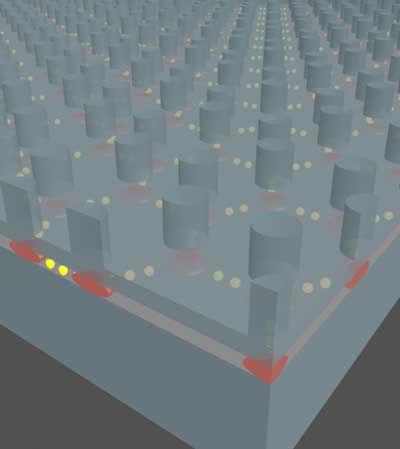
Schematic diagram of artificial graphene in a semiconductor
Schematic diagram of artificial graphene in a semiconductor. Etched pillars define the positions of quantum dots (red puddles) arranged in an hexagonal lattice. When the spacing between the quantum dots is sufficiently small, electrons can move between them. (Image: Diego Scarabelli/Columbia Engineering)
The discovery of graphene in the early 2000s generated tremendous excitement in the physics community not only because it was the first real-world realization of a true two-dimensional material but also because the unique atomic arrangement of the carbon atoms in graphene provided a platform for testing new quantum phenomena that are difficult to observe in conventional materials systems. With its unusual electronic properties¾its electrons can travel great distances before they are scattered¾graphene is an outstanding conductor. These properties also display other unique characteristics that make electrons behave as if they are relativistic particles that move close to the speed of light, conferring upon them exotic properties that “regular,” non-relativistic electrons do not have.
But graphene, a natural substance, comes in only one atomic arrangement: the positions of the atoms in the graphene lattice are fixed, and thus all experiments on graphene must adapt to those constraints. On the other hand, in artificial graphene the lattice can be engineered over a wide range of spacings and configurations, making it a holy grail of sorts for condensed matter researchers because it will have more versatile properties than the natural material.
“This is a rapidly expanding area of research, and we are uncovering new phenomena that couldn’t be accessed before,” says Shalom Wind, faculty member of the department of applied physics and applied mathematics and co-author of the study. “As we explore novel device concepts based on electrical control of artificial graphene, we can unlock the potential to expand frontiers in advanced optoelectronics and data processing.”
“This work is really a major advance in artificial graphene. Since the first theoretical prediction that system with graphene-like electronic properties may be artificially created and tuned with patterned 2D electron gas, no one had succeeded, until the Columbia work, in directly observing these characteristics in engineered semiconductor nanostructures,” says Steven G. Louie, professor of physics, University of California, Berkeley. “Previous work with molecules, atoms and photonic structures represent far less versatile and stable systems. The nanofabricated semiconductor structures open up tremendous opportunities for exploring exciting new science and practical applications.”
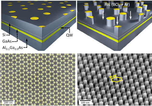
Nanofabrication of artificial graphene in a semiconductor
Nanofabrication of artificial graphene in a semiconductor. The green layer represents the 2D sheet where the electrons can move. Nanolithography and etching form small pillars beneath which lie the quantum dots arranged in an hexagonal lattice. Scanning electron micrographs at the bottom show the hexagonal array, with a period of only 50 nanometers, from the top and at an angle. (Image: Diego Scarabelli/Columbia Engineering)
The researchers used the tools of conventional chip technology to develop the artificial graphene in a standard semiconductor material, gallium arsenide. They designed a layered structure so that the electrons could move only within a very narrow layer, effectively creating a 2D sheet. They used nanolithography and etching to pattern the gallium arsenide: the patterning created a hexagonal lattice of sites in which the electrons were confined in the lateral direction. By placing these sites, which could be thought of as “artificial atoms,” sufficiently close to one another (~ 50 nanometers apart), these artificial atoms could interact quantum mechanically, similar to the way atoms share their electrons in solids.
The team probed the electronic states of the artificial lattices by shining laser light on them and measuring the light that was scattered. The scattered light showed a loss of energy that corresponded to transitions in the electron energy from one state to another. When they mapped these transitions, the team found that they were approaching zero in a linear fashion around what is called the “Dirac point” where the electron density vanishes, a hallmark of graphene.
This artificial graphene has several advantages over natural graphene: for instance, researchers can design variations into the honeycomb lattice to modulate electronic behavior. And because the spacing between the quantum dots is much larger than the inter-atomic spacing in natural graphene, researchers can observe even more exotic quantum phenomena with the application of a magnetic field.
The discovery of new low-dimensional materials, such as graphene and other ultrathin, layered van der Waals films that exhibit exciting new physical phenomena that were previously inaccessible, laid the groundwork for this study. “What was really critical to our work was the impressive advancements in nanofabrication,” Pinczuk notes. “These offer us an ever-increasing toolbox for creating a myriad of high-quality patterns at nanoscale dimensions. This is an exciting time to be a physicist working in our field.”
Source: Columbia University