Celulele solare cu o schimbare cuantică(Solar cells with a quantum shift)

Echipa a investigat un feroelectric organic cu o polarizare cuantică puternică pentru a-și explora capabilitățile de schimbare-curent. Compus din inele aromatice aromatice tetrathiafulvalene (TTF) și p-cloranil (CA), acest complex trece printr-o separare instantanee a încărcăturii când este răcită la aproximativ -200 de grade Celsius și este deosebit de sensibilă la lumina soarelui.

Posted: Dec 08, 2017

Solar cells with a quantum shift

(Nanowerk News) A much quicker, less wasteful way to extract current from solar cells that uses a quantum-mechanical process has been demonstrated by RIKEN researchers (Nature Communications, „Shift current photovoltaic effect in a ferroelectric charge-transfer complex”).

When sunlight strikes a typical solar panel, it creates pairs of electrons and positively charged holes. Normally, an electric field is used to separate these charges and produce electrical power, but this approach requires charges that have high mobilities and lifetimes, which makes it hard to develop new photovoltaic materials.
An alternative approach for extracting current from solar cells involves exploiting the symmetry of the repeating structural units that make up crystals. Certain semiconductors lack ‘inversion’ symmetry—meaning that if their atoms are flipped about the center of the repeating unit, a different atomic arrangement will be produced.
For such semiconductors, light-induced transitions of charges to excited states become unbalanced, which creates a ‘shift current’ along a specific crystal direction. This shift current propagates rapidly and with less energy loss than a current generated by applying an electric field. But shift currents usually generate insufficient photovoltaic power for practical uses.
Now, Masao Nakamura from the RIKEN Center for Emergent Matter Science and colleagues have overcome this shortcoming by using ferroelectric organic molecules that spontaneously separate their positive and negative charges. Because ferroelectric materials naturally disrupt inversion symmetry, they have potentially large shift currents—particularly when charge separation occurs due to quantum-mechanical differences in the covalent bonds holding a crystal together.
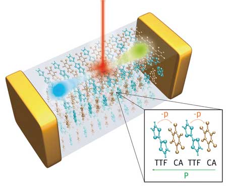
The team investigated an organic ferroelectric with strong quantum polarization to explore its shift-current capabilities. Composed of alternately stacked tetrathiafulvalene (TTF) and p-chloranil (CA) aromatic rings (Fig. 1), this complex undergoes instantaneous charge separation when cooled to around -200 degrees Celsius and is particularly sensitive to sunlight.
An organic charge-transfer complex can generate dissipation-free solar power thanks to quantum-based polarization effects
Figure 1: An organic charge-transfer complex can generate dissipation-free solar power thanks to quantum-based polarization effects. (Image: RIKEN Center for Emergent Matter Science)
“Most ferroelectric materials need light with energy in the ultraviolet region to excite carriers over a large band gap,” says Nakamura. “With TTF–CA, the band gap is narrow and responds to visible and infrared light, which is really important for applications like solar cells.”
When the researchers measured the photovoltaic properties of the organic complex, they were taken aback by the amount of shift current generated—nearly ten times higher than comparable oxide ferroelectrics. The quantum-based charge transfer dramatically improved solar output power and allowed the current to travel as far as 200 micrometers before dissipating.
Because the shift-current effects in TTF–CA are so sizeable, Nakamura expects that it could be used as a platform to implement this photoelectric conversion in next-generation devices. “We’ll be looking at other ferroelectrics to try for room-temperature operation,” he says. “And we think we can improve extraction efficiency by employing thin-film device structures.”
Source: RIKEN

Catalizatorul de hidrogen superior crește doar în acest fel(Superior hydrogen catalyst just grows that way)

solicitat un brevet comun pentru procesul de tipărire prin pulverizare, care utilizează disulfură de molibden ieftină. Suprafața mărită a „frunzei” se creează de trei ori mai multe puncte de contact catalitic ca și alte structuri de disulfură de molibden, iar noua creație poate suporta temperaturi mai ridicate decât platina, fără sinterizarea și învelirea celulei.
Lucrarea ( Materiale avansate , „MoS 2 deformate structural pentru stabilitate electrochimică, rezistentă la temperatură și reacție de evoluție a hidrogenului foarte eficient” ) face parte dintr-un efort de a propulsa mai ieftin autovehicule pe bază de hidrogen, de dorit deoarece emit apă mai degrabă decât monoxid de carbon dioxid de carbon.

Posted: Dec 05, 2017

Superior hydrogen catalyst just grows that way

(Nanowerk News) Replacing your everyday gas guzzler with a hydrogen fueled car could drastically reduce your carbon footprint. So why don’t we all make the switch?

One of reasons we don’t is the expensive platinum catalyst required to operate hydrogen fuel cells efficiently.
Research led by Sandia National Laboratories and the University of California, Merced aim at bringing down the cost of hydrogen fuel cells by using a dirt-cheap compound to create an uneven surface that resembles a plant’s leaves. The additional area helps catalyze hydrogen almost as efficiently as platinum.
a 'flowering' hydrogen catalyst
These inorganic ‘flowers,’ color added, were created by Sandia National Laboratories researcher Stanley Chou and University of California, Merced colleague Vincent Tung in a spray-printing process that uses molybdenum disulfide to create a ‘flowering’ hydrogen catalyst far cheaper than platinum and reasonably close in efficiency. (Image: Sandia National Laboratories)
Lead researchers Stanley Chou, a Sandia materials scientist, and UC Merced’s Vincent Tung have applied for a joint patent for the spray-printing process, which uses inexpensive molybdenum disulfide. The increased surface area of the rippling „leaf” creates three times as many catalytic contact points as other molybdenum disulfide structures, and the new creation can handle higher temperatures than platinum without sintering and gumming up the cell.
The work (Advanced Materials, „Structurally Deformed MoS2 for Electrochemically Stable, Thermally Resistant, and Highly Efficient Hydrogen Evolution Reaction”) is part of an effort to more cheaply power hydrogen-fueled cars, desirable because they emit water rather than carbon monoxide or carbon dioxide.

Nature as an ally

The production method uses nature as an ally rather than a hindrance, Chou said. „In traditional thinking, forces such as gravity, viscosity and surface tension must be overcome to achieve the manufactured shapes you desire. We thought, instead of thinking these forces as limitations, why not use them to do something useful? So, we did.”
Tung said the method uses natural processes to produce materials for extremely inexpensive fuel cell terminals to liberate hydrogen. „The printing process also allows for continued deposition, with the ability to scale for industry,” he said.
The team mixed molybdenum disulfide with water and used the printing process to expel micron-size droplets into an enclosed area about 2 feet high. As they dropped, the droplets first separated into nanoscopic subunits. These dried further as they fell, their shrinking volume producing an uneven 3-D surface much like the leaves of plants, with tiny ridges, hills, canals, caves and tunnels. Landing on a substrate and on each other, the „leaves” were still moist enough to bond as though attached at critical points by tiny droplets of glue. Thus, the nanostructures did not lose their individuality but instead, by maintaining their identities, created tiny tunnels within and between them that permitted extraordinary access for atoms of hydrogen to seek their freedom from chemical bonds.
The inspiration for creating a bio-inspired 3-D form arose from studying the cuticle folding process, a mechanism used by plants for controlling diffusion and permeability on leaf surfaces, Chou said.
„We see our catalyst as an inorganic material acting like a plant. The nanostructures, like leaves, are varied in shape, with tiny rises and falls,” he said. „The structures take in an external material to produce hydrogen rather than oxygen, and one day may be powered by sunlight.” Right now, very low-voltage electricity does the job.
Doubts about the strength of structure formed in such a serendipitous manner, Tung recounted, were settled when a 170-pound student unwittingly trod upon one of the first molybdenum disulfide-catalyst creations when it accidentally fell to the floor. A few hundred nanometers thick, it rested upon a centimeter-square carbon substrate but was otherwise unprotected. Elecromicroscopic investigation showed the tiny structure to be undamaged. The „leaves” also have proved to be long lasting, continuing to produce hydrogen for six months.
Source: Sandia National Laboratories

Valsul cuantic al electronilor indică următoarea generație de jetoane(The quantum waltz of electrons hints at the next generation of chips)

Proiectele lor de cercetare, care au fost publicate recent în ACS Nano și în Nature Communications ( „Rezolvarea divizării spinului în banda de conducere a monostratului MoS 2 ” ), confirmă faptul că materiale precum grafen (C), molibdenită (MoS 2 ) și diselenă de wolfram WSe 2 ) oferă, fie singure, fie prin combinarea unor caracteristici ale acestora, noi perspective în domeniul electronicii – perspective care ar putea duce în cele din urmă la chips-uri mai mici care generează mai puțină căldură.

Posted: Dec 05, 2017

The quantum waltz of electrons hints at the next generation of chips

(Nanowerk News) A group of spintronics researchers at EPFL is using new materials to reveal more of the many capabilities of electrons. The field of spintronics seeks to tap the quantum properties of „spin,” the term often used to describe one of the fundamental properties of elementary particles – in this case, electrons. This is among the most cutting-edge areas of research in electronics today.

Researchers working in the Laboratory of Nanoscale Electronics and Structures (LANES), which is run by Professor Andras Kis, were able to quantify these quantum properties for a category of two-dimensional semiconductors called transition metal dichalcogenides, or TMDCs.
Their research projects, which were published recently in ACS Nano and in Nature Communications („Resolving the spin splitting in the conduction band of monolayer MoS2„), confirm that materials like graphene (C), molybdenite (MoS2) and tungsten diselenide (WSe2) offer, either alone or by combining some of their characteristics, new perspectives for the field of electronics – perspectives that could ultimately lead to smaller chips that generate less heat.
„With the methods we’ve recently developed, we’ve shown that it is possible to access the spin in these TMDC materials, quantify it and use it to introduce new functionalities,” says Kis.
This all takes place at an extremely small scale. In order to access these quantum properties, the researchers must work with high quality materials. „If we want to examine certain characteristics of electrons, including their energy, we need to be able to watch them move over relatively long distances without there being too much dispersion or disruption,” explains Kis.

In the form of waves

The researchers’ method allows them to obtain samples of sufficient quality both to observe how electrons move around in the form of waves and to quantify their energy.
But the LANES team was also able to access another quantum property. Spins of electrons and holes in this type of a 2D semiconductor can be in one of two states, which are conventionally described as being oriented upward – spin up – or downward – spin down. Their energy will be slightly different in each of these two states. That’s called spin splitting, and the EPFL researchers have measured it for the first time for electrons in TMDC materials.
In the second publication, the researchers wrote about how they used the spin splitting in a TMDC in order to introduce polarized spin currents in graphene without using a magnetic field.
These discoveries are a step forward for the emerging field of spintronics and make it increasingly likely that a different property of charge carriers – i.e. spin, in addition to the electrical charge – will play a role in tomorrow’s electronic devices.
Source: Ecole Polytechnique Fédérale de Lausanne

Hibridul electrolit mărește supercapacitanța în nanofibrele verticale de grafen(Hybrid electrolyte enhances supercapacitance in vertical graphene nanosheets)

VGN-urile sunt rețele de nanomateriale de carbon 3-D care cresc în rânduri de foi verticale, oferind o suprafață mare pentru o capacitate mai mare de stocare a încărcăturii. De asemenea, numite nanowale de carbon sau nanoflaze de grafen, VGN oferă promisiuni în sistemele de stocare a energiei de mare putere, celulele de combustie, senzorii bio și dispozitivele magnetice, printre altele.

Posted: Dec 05, 2017

Hybrid electrolyte enhances supercapacitance in vertical graphene nanosheets

(Nanowerk News) Supercapacitors can store more energy than and are preferable to batteries because they are able to charge faster, mainly due to the vertical graphene nanosheets (VGNs) that are larger and positioned closer together. VGNs are 3-D networks of carbon nanomaterial that grow in rows of vertical sheets, providing a large surface area for greater charge storage capacity. Also called carbon nanowalls or graphene nanoflakes, VGNs offer promise in high-power energy storage systems, fuel cells, bio sensors and magnetic devices, amongst others.

Using VGNs as the material for supercapacitor electrodes offers advantages due to their intriguing properties such as an interconnected porous nanoarchitecture, excellent conductivity, high electrochemical stability, and its array of nanoelectrodes. Advantages of VGNs can be enhanced depending on how the material is grown, treated and prepared to work with electrolytes.
„Performance of a supercapacitor not only depends on the geometry of electrode material, but also depends on the type of electrolyte and its interaction with the electrode,” said Subrata Ghosh of the Indira Gandhi Centre for Atomic Research at Homi Bhabha National Institute. „To improve the energy density of a device, [electric] potential window enhancement will be one key factor.”
Scanning electron micrograph of vertical graphene nanosheets with different magnifications
(a)–(c) Scanning electron micrograph of vertical graphene nanosheets with different magnifications. (d) Magnified image of single nanosheets after KOH activation, showing nanopore formation. (© AIP)
In a paper published this week in the Journal of Applied Physics („Enhanced supercapacitance of activated vertical graphene nanosheets in hybrid electrolyte”), Ghosh and a team of researchers discovered ways to improve the material’s supercapacitance properties.
According to modeling, VGNs should be able to provide high charge storage capabilities, and the scientific community is trying to unlock the keys to reaching the levels of efficiency that are theoretically available. Needed improvements to be viable include, for instance, greater capacitance per unit of material, greater retention, less internal resistance, and greater electrochemical voltage ranges (operating potential windows).
„Our motivation was to improve VGN performance,” Ghosh said. „We have taken two strategies. One is inventing a novel electrolyte, and another is improving the VGN structure by chemical activation. The combination of both enhances the charge storage performance remarkably.”
The researcher team treated VGNs with potassium hydroxide (KOH) to activate the electrodes and then allowed the treated electrodes to interact with a hybrid electrolyte, testing the formation of the electric double layer at the electrode/electrolyte interface. They also examined the morphology, surface wettability, columbic efficiency and areal capacitance of VGN.
The novel electrolyte they created is a hybrid that combines the advantages of aqueous and organic electrolytes for a novel hybrid organo-aqueous version that works to increase supercapacitor performance of VGNs. Using an organic salt, Tetraethylammonium tetrafluoroborate (TEABF4), in an acidic aqueous solution of sulfuric acid (H2SO4), they created an electrolyte that extended the device’s operating window.
Improvement of VGN architecture was associated with the process of KOH activation, which grafted the oxygen functional group onto the electrode, improved electrode wettability, reduced internal resistance and provided a fivefold improvement in capacitance of the VGNs. The activation approach in the paper can be applied to other supercapacitor devices that are based on nanoarchitecture, Ghosh said.
„Aqueous and organic electrolytes are extensively used, but they have their own advantages and disadvantages,” he said. „Hence the concept of hybrid electrolyte arises.”
Source: American Institute of Physics

Nanowires noi sunt doar câteva atomi grosime(New nanowires are just a few atoms thick)

Materialele bidimensionale – materialele depuse în straturi cu grosimea de numai câteva atomi – promit atât elementele electronice de înaltă performanță, cât și electronice flexibile și transparente, care ar putea fi stratificate pe suprafețele fizice pentru a face computerele omniprezente.
Cel mai cunoscut material 2-D este grafenul, care este o formă de carbon, dar recent cercetătorii au investigat alte materiale 2-D, cum ar fi disulfura de molibden, care au propriile lor avantaje distincte.

Posted: Dec 04, 2017

New nanowires are just a few atoms thick

(Nanowerk News) Two-dimensional materials – materials deposited in layers that are only a few atoms thick – are promising for both high-performance electronics and flexible, transparent electronics that could be layered onto physical surfaces to make computing ubiquitous.

The best-known 2-D material is graphene, which is a form of carbon, but recently researchers have been investigating other 2-D materials, such as molybdenum disulfide, which have their own, distinct advantages.
A slight mismatch between the hexagonal structures of molybdenum disulfide and tungsten diselenide creates a strain
A slight mismatch between the hexagonal structures of molybdenum disulfide and tungsten diselenide creates a strain that can be released by the formation of a „5|7 dislocation,” in which two hexagons collapse to form a pentagon and a heptagon. Reactions with molybdenum disulfide in the environment cause the dislocation to move deeper into the tungsten diselenide, drawing a nanowire of molybdenum disulfide behind it. (Image courtesy of the researchers)
Producing useful electronics, however, requires integrating multiple 2-D materials in the same plane, which is a tough challenge. In 2015, researchers at King Abdullah University in Saudi Arabia developed a technique for depositing molybdenum disulfide (MoS2) next to tungsten diselenide (WSe2), with a very clean junction between the two materials. With a variation of the technique, researchers at Cornell University then found that they could induce long, straight wires of MoS2 – only a few atoms in diameter– to extend into the WSe2, while preserving the clean junction.
The researchers contacted Markus Buehler, the McAfee Professor of Engineering in MIT’s Department of Civil and Environmental Engineering, who specializes in atomic-level models of crack propagation, to see if his group could help explain this strange phenomenon.
In the latest issue of Nature Materials („Sub-nanometre channels embedded in two-dimensional materials”), the King Abdullah, Cornell, and MIT researchers team with colleagues at Academia Sinica, the Taiwanese national research academy, and Texas Tech University to describe both the material deposition method and the mechanism underlying the formation of the MoS2nanowires, which the MIT researchers were able to model computationally.
„The manufacturing of new 2-D materials still remains a challenge,” Buehler says. „The discovery of mechanisms by which certain desired material structures can be created is key to moving these materials toward applications. In this process, the joint work of simulation and experiment is critical to make progress, especially using molecular-level models of materials that enable new design directions.”

Wired up

The ability to create long, thin MoS2 channels in WSe2 could have a number of applications, the researchers say.
„Based on [the materials’] electrical properties and optical properties, people are looking at using MoS2 and WSe2 for solar cells or for water splitting based on sunlight,” says Gang Seob Jung, an MIT graduate student in civil and environmental engineering and a coauthor on the new paper. „Most of the interesting stuff happens at the interface. When you have not just the one interface – if there are many nanowire interfaces – it could improve the efficiency of a solar cell, even if it’s quite random.”
But the theoretical explanation of the molecular mechanism underlying the nanowires’ formation also raises the hope that their formation could be controlled, to enable the assembly of atom-scale electronic components.
„Two-D materials, one of the most promising candidates for future electronics, ultimately need to beat silicon-based devices, which have achieved a few nanometers in size already,” says Yimo Han, a Cornell graduate student in chemistry and first author on the paper. „Two-D materials are the thinnest in the vertical direction but still span a quite large area in the lateral dimensions. We made the thinnest dislocation-free channels in 2-D materials, which is a big step toward subnanometer electronic devices out of 2-D materials.”

Propagating polygons

In a 2-D crystal, both MoS2 and WSe2 naturally arrange themselves into hexagons in which the constituent elements – molybdenum and sulfur or tungsten and selenium – alternate. Together, these hexagons produce a honeycomb pattern.
The Cornell researchers’ fabrication technique preserves this honeycomb pattern across the junction between materials, a rare feat and one that’s very useful for electronics applications. Their technique uses chemical vapor deposition, in which a substrate – in this case, sapphire – is exposed to gases carrying chemicals that react to produce the desired materials.
The natural sizes of the MoS2 and WSe2 hexagons are slightly different, however, so their integration puts a strain on both crystals, particularly near their junction. If a pair of WSe2hexagons right at the MoS2 junction convert into a hexagon matched with a heptagon (a seven-sided polygon), it releases the strain.
This so-called 5|7 dislocation creates a site at which an MoS2 particle can attach itself. The resulting reaction inserts a molybdenum atom into the pentagon, producing a hexagon, and breaks the heptagon open. Sulfur atoms then attach to the heptagon to form another 5|7 dislocation. As this process repeats, the 5|7 dislocation moves deeper into WSe2 territory, with a nanowire extending behind it. The pattern in which the strain on the mismatched hexagons relaxes and recurs ensures that the dislocation progresses along a straight line.
Source: MIT

Studiul confirmă faptul că materialele din cupru au dungi fluctuante care pot fi legate de supraconductivitatea la temperaturi înalte(Study confirms that cuprate materials have fluctuating stripes that may be linked to high-temperature superconductivity)

au aratat ca superconductorii pe baza de cupru sau cupati – prima clasa de materiale gasite sa transporte electricitate fara pierderi la temperaturi relativ ridicate – contin dungi fluctuante de electroni încărcați-vă și rotiți-vă ca pe niște râuri pe pământ dur.
Dungile sunt zone unde electronii se încarcă, creează benzi de încărcare negativă sau aliniază spini pentru a crea benzi de magnetism. Erau cunoscuți anterior ca existenți în superconductori de cupru la temperaturi apropiate de zero absolut, deși în această friguroasă profundă dungile nu s-au mișcat în jurul lor și rolul lor exact în superconductivitate

Posted: Dec 01, 2017

Study confirms that cuprate materials have fluctuating stripes that may be linked to high-temperature superconductivity

(Nanowerk News) Scientists at the Department of Energy’s SLAC National Accelerator Laboratory and Stanford University have shown that copper-based superconductors, or cuprates – the first class of materials found to carry electricity with no loss at relatively high temperatures – contain fluctuating stripes of electron charge and spin that meander like rivulets over rough ground.

The stripes are zones where electrons either pile up, creating bands of negative charge, or align their spins to create bands of magnetism. They were previously known to exist in cuprate superconductors at temperatures near absolute zero, although in this deep chill the stripes did not move around and their exact role in superconductivity – do they boost or squelch it? – has been unclear.
Now the researchers have computationally demonstrated for the first time that these stripes also exist at high temperatures, but they are subtle and fluctuate in a way that could only be discovered through numerical computer simulations of a precision and scale not done before. The scientists described their study in Science („Numerical evidence of fluctuating stripes in the normal state of high-Tc cuprate superconductors”).
text
An animation based on computer simulations shows stripes of electron charge (white atoms) and spin (red and blue atoms) in a copper-based superconducting material. The stripes are zones where electrons either pile up, creating bands of negative charge, or align their spins (arrows) in a particular pattern to create bands of magnetism. A computational study by researchers at SLAC and Stanford shows these stripes are present in a subtle, fluctuating form at high temperatures. The results will help researchers test theories about how stripes may be related to high-temperature superconductivity. (Image: Farrin Abbott/SLAC National Accelerator Laboratory)
“There’s reason to think that stripes of charge and spin may be intimately tied to the emergence of high-temperature superconductivity in these materials, which was discovered 30 years ago but so far is not understood or explained,” said Edwin Huang, a physics graduate student at Stanford and at the Stanford Institute for Materials and Energy Sciences (SIMES) at SLAC.
“This discovery of fluctuating stripes in a realistic computer model will give us a way to test the many theories about how stripes are related to superconductivity,” Huang said. “We think our results will be useful for scientists doing experimental studies of these materials, and they’ll also help develop and refine the computational techniques that go hand in hand with theory and experiments to push the field forward.”
The results also apply to other novel materials, said SIMES Director Thomas Devereaux. “Materials that spontaneously develop this sort of non-uniform structure are quite commonplace, including magnets and ferroelectrics,” he said. “It can even be thought of as a signature of ‘quantum’ materials, whose surprising properties are produced by electrons that cooperate in unexpected ways. Our numerical results demonstrate that this phenomenon can generally be related to strong interactions between electron charges and spin.”

A Mysterious Phenomenon

In conventional electrical conductors, current is transmitted by electrons acting individually. But in superconductors, electrons pair up to transmit current with virtually no loss.
For 75 years after their discovery, all known superconductors operated only at temperatures close to absolute zero, limiting the way they could be used.
That changed in 1986, when scientists discovered that cuprates could superconduct at much higher (although still quite chilly) temperatures. In fact, certain cuprate compounds are superconducting at temperatures higher than 100 kelvins, or minus 173 degrees Celsius, allowing development of superconducting technologies that can be chilled with liquid nitrogen.
But researchers are still far from their goal of finding superconductors that operate at close to room temperature for highly efficient power lines, maglev trains and other applications that could have a profound impact on society. Without a fundamental understanding of how high-temperature superconductors work, progress has been slow.
Computer modeling is a critical tool for achieving that understanding. Models are sets of mathematical equations based on physics that theorists create and continually refine to simulate a material’s behavior using computer algorithms. They check their models against observations and experimental results to make sure they’re on the right track.
In this case, the team modeled electron behavior and interactions in one of a cuprate’s copper oxide layers, which is where the interesting physics happens, said SIMES staff scientist Brian Moritz. The calculations were run on Stanford’s Sherlock supercomputer cluster at SLAC and at the DOE’s National Energy Research Scientific Computing Center in Berkeley.
The results were in good agreement with data from neutron scattering experiments on a variety of cuprates, the scientists said, confirming that their simulations accurately capture the electronic physics of these materials.

A More Accurate Model

This is the first time the high-temperature behavior of cuprates has been simulated with a realistic model that covers a large enough area of the material to see fluctuating stripes, Huang said. This larger scale also makes the calculations more accurate.
“There was a fine balance we needed to strike,” he said. “These are extremely computationally demanding calculations. But if you simulate the behavior of smaller areas, you won’t be able to see any stripes that emerge. That was the primary limitation of previous studies.”
The simulations show that stripes emerge at temperatures up to 600 degrees Celsius and in a wide range of doping conditions, where compounds are added to a material to tweak its electronic behavior, and so they appear to be a universal trait of cuprate superconductors, the researchers said.
“The idea that there are fluctuating stripes in cuprates is not new, but it has been a controversial topic for many years,” Huang said. “What’s new here is that we can support their existence using unbiased computation on a realistic model of these materials.”
One thing the study does not do, he added, is answer the question of whether or how the fluctuating stripes figure into superconductivity: “That is the direction we want to head toward.”
Source: By Glennda Chui, SLAC National Accelerator Laboratory

Graphene nano penseta poate apuca biomolecule individuale(Graphene nano tweezers can grab individual biomolecules)

Graphene, un material fabricat dintr-un singur strat de atomi de carbon, a fost descoperit cu mai mult de un deceniu în urmă și a încântat cercetătorii cu gama sa de proprietăți uimitoare care s-au găsit utilizări în multe aplicații noi, de la microelectronică la celule solare.
Pensetele de grafen, dezvoltate la Universitatea din Minnesota, sunt mult mai eficiente în captarea particulelor în comparație cu alte tehnici folosite în trecut, datorită faptului că grafenul monostrat este un singur atom gros. a realizat penseta de grafen prin crearea unei structuri sandwich în care un material subțire izolant numit dioxid de hafniu este așezat între un metal electrodul pe o parte și grafenul pe cealaltă. Hidroxidul de hafniu este un material utilizat în mod curent în microcipurile avansate de astăzi.

Posted: Dec 01, 2017

Graphene nano tweezers can grab individual biomolecules

(Nanowerk News) Researchers from the University of Minnesota College of Science and Engineering have found yet another remarkable use for the wonder material graphene—tiny electronic “tweezers” that can grab biomolecules floating in water with incredible efficiency. This capability could lead to a revolutionary handheld disease diagnostic system that could be run on a smart phone.

Graphene, a material made of a single layer of carbon atoms, was discovered more than a decade ago and has enthralled researchers with its range of amazing properties that have found uses in many new applications from microelectronics to solar cells.
The graphene tweezers developed at the University of Minnesota are vastly more effective at trapping particles compared to other techniques used in the past due to the fact that monolayer graphene is a single atom thick.
The research study was published in Nature Communications („Graphene-edge dielectrophoretic tweezers for trapping of biomolecules”).
Atomically sharp edges of electrically driven graphene can act as tweezers that rapidly trap biomolecules from the surrounding solution
Atomically sharp edges of electrically driven graphene can act as “tweezers” that rapidly trap biomolecules from the surrounding solution. (Image: In-Ho Lee, University of Minnesota)

The world’s sharpest tweezers

The physical principle of tweezing or trapping nanometer-scale objects, known as dielectrophoresis, has been known for a long time and is typically practiced by using a pair of metal electrodes. From the viewpoint of grabbing molecules, however, metal electrodes are very blunt. They simply lack the “sharpness” to pick up and control nanometer-scale objects.
“Graphene is the thinnest material ever discovered, and it is this property that allows us to make these tweezers so efficient. No other material can come close,” said research team leader Sang-Hyun Oh, a Sanford P. Bordeau Professor in the University of Minnesota’s Department of Electrical and Computer Engineering. “To build efficient electronic tweezers to grab biomolecules, basically we need to create miniaturized lightning rods and concentrate huge amount of electrical flux on the sharp tip. The edges of graphene are the sharpest lightning rods.”
The team also showed that the graphene tweezers could be used for a wide range of physical and biological applications by trapping semiconductor nanocrystals, nanodiamond particles, and even DNA molecules. Normally this type of trapping would require high voltages, restricting it to a laboratory environment, but graphene tweezers can trap small DNA molecules at around 1 Volt, meaning that this could work on portable devices such as mobile phones.
Using the University of Minnesota’s state-of-the-art nanofabrication facilities at the Minnesota Nano Center, electrical and computer engineering Professor Steven Koester’s team made the graphene tweezers by creating a sandwich structure where a thin insulating material call hafnium dioxide is sandwiched between a metal electrode on one side and graphene on the other. Hafnium dioxide is a material that is commonly used in today’s advanced microchips.
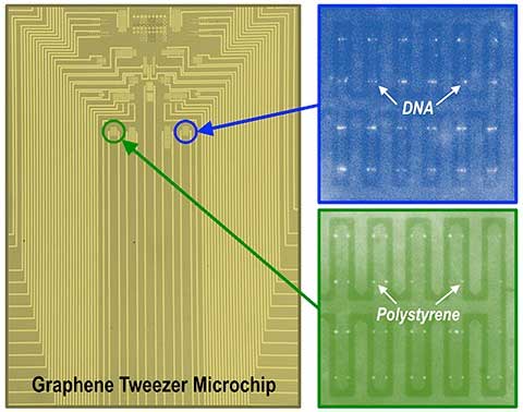
Fluorescence images show DNA molecules and polystyrene nanoparticles trapped on a graphene chip
The University of Minnesota team produced a microchip containing a large array of graphene electronic tweezers. Fluorescence images show DNA molecules and polystyrene nanoparticles trapped on the chip. (Image: Barik et al., University of Minnesota)
“One of the great things about graphene is it is compatible with standard processing tools in the semiconductor industry, which will make it much easier to commercialize these devices in the future,” said Koester, who led the effort to fabricate the graphene devices.
“Since we are the first to demonstrate such low-power trapping of biomolecules using graphene tweezers, more work still needs to be done to determine the theoretical limits for a fully optimized device,” said Avijit Barik, a University of Minnesota electrical and computer engineering graduate student and lead author of the study. “For this initial demonstration, we have used sophisticated laboratory tools such as a fluorescence microscope and electronic instruments. Our ultimate goal is to miniaturize the entire apparatus into a single microchip that is operated by a mobile phone.”

Tweezers that can ‘feel’

Another exciting prospect for this technology that separates graphene tweezers from metal-based devices is that graphene can also “feel” the trapped biomolecules. In other words, the tweezers can be used as biosensors with exquisite sensitivity that can be displayed using simple electronic techniques.
“Graphene is an extremely versatile material,” Koester said. “It makes great transistors and photodetectors, and has the potential for light emission and other novel biosensor devices. By adding the capability to rapidly grab and sense molecules on graphene, we can design an ideal low-power electronics platform for a new type of handheld biosensor.”
Oh agrees that the possibilities are endless.
“Besides graphene, we can utilize a large variety of other two-dimensional materials to build atomically sharp tweezers combined with unusual optical or electronic properties,” said Oh. “It is really exciting to think of atomically sharp tweezers that can be used to trap, sense, and release biomolecules electronically. This could have huge potential for point-of-care diagnostics, which is our ultimate goal for this powerful device.”
Source: University of Minnesota College of Science and Engineering

Metamaterial cu o întorsătură(Metamaterial with a twist)

cercetatorii de la KIT au reusit sa creeze un metamaterial din blocuri de constructii cubice care raspunde fortelor de compresie printr-o rotatie.

Posted: Dec 01, 2017

Metamaterial with a twist

(Nanowerk News) Using 3D printers for the microrange, researchers of KIT have succeeded in creating a metamaterial from cubic building blocks that responds to compression forces by a rotation. Usually, this can only be achieved by transmission using a crankshaft, for instance. The sophisticated design of bars and ring structures and the underlying mathematics are now presented in the latest issue of Science („Three-dimensional mechanical metamaterials with a twist”).

Forces from above are transmitted to the vertical ring structures via bars. The rotation of the rings exerts forces onto the corners of the horizontal planes of the cube
Forces from above are transmitted to the vertical ring structures via bars. The rotation of the rings exerts forces onto the corners of the horizontal planes of the cube. (T. Frenzel/KIT)
“If a force is exerted from above onto a material, the latter deforms in various ways. It may be bulged, compressed, or bent,” says Martin Wegener, Professor of the Institute of Applied Physics and Director of the Institute of Nanotechnology of KIT. “According to the valid rules of mechanics, however, it will not rotate,” he adds. His staff member Tobias Frenzel and colleagues, however, have now succeeded in designing a filigree cubic structure that reacts to loading by a rotation around its axis.
“By means of a computer simulation, we first developed a design with this new mechanical property that has not been described so far,” Frenzel, the first author of the study, explains. “Our calculations revealed that the desired behavior is shown by a complex chiral structure, i.e. a structure that cannot be mapped to its mirror image, similar to the left and the right hand.”
The filigree cubes calculated by Frenzel and his team consist of bars and rings that are connected to each other in a certain pattern. “The arms that connect the ring structures with the corners of the cube move vertically downwards under load. This movement leads to a rotation of the rings,” Frenzel explains. “These rotation movements, in turn, transmit forces to the corners of the horizontal planes of the cube, such that the complete structure starts to twist around its axis.”
Towers of up to 500 chiral cubic structures rotated around their axis under load
Towers of up to 500 chiral cubic structures rotated around their axis under load. (T. Frenzel/KIT)
Towers of up to 500 chiral cubic structures rotated around their axis under load. Achiral structures do not exhibit this behavior. (T. Frenzel/KIT)
Then, the team produced towers of the above cubic structures of variable sizes, strengths, and pieces using a 3D microprinting method established at KIT. The edge length of the cubes ranged from 100 to 500 µm. The researchers built towers of 4 to 500 cubes and 2 mm height. To check their theory, they also built towers of achiral cubes, i.e. cubes that can be mapped to their mirror image.
The scientists found that towers assembled from chiral blocks started to rotate around their axis under the impact of force. “We measured a rotation by up to two degrees per percent of deformation,” Frenzel says. The towers made of achiral cubic structures did not exhibit this rotation. The researchers also found that the stiffness of the towers increased with the number of cubes, although the dimensions of the individual components decreased proportionally.
While towers of up chiral cubic structures rotated around their axis under load, achiral structures do not exhibit this behavior
While towers of up chiral cubic structures rotated around their axis under load, achiral structures do not exhibit this behavior. (T. Frenzel/KIT)
According to Tobias Frenzel, there is still a far way to go to application. Work was inspired by the team’s previous studies of elastic “invisibility cloaks.” These might be used to buffer shock waves of earthquakes or divert them around historic buildings.
Source: Karlsruhe Institute of Technology

Apărarea finală împotriva hackerilor poate avea doar câteva atomi grosime(The ultimate defense against hackers may be just a few atoms thick)

La grosimea monostratului, acest material are proprietățile optice ale unui semiconductor care emite lumină, dar la mai multe straturi proprietățile se schimbă și materialul nu mai emite lumină. Această proprietate este unică pentru acest material”, a spus el. Prin reglarea procesului de creștere a materialului, pelicula subțire rezultată este gravată cu regiuni aleatoare care, în mod alternativ, emit sau nu emite lumină. Când este expus la lumină, acest model se traduce într-o cheie de autentificare unică, care ar putea securiza componentele hardware la un cost minim.

Posted: Nov 29, 2017

The ultimate defense against hackers may be just a few atoms thick

(Nanowerk News) The next generation of electronic hardware security may be at hand as researchers at New York University Tandon School of Engineering introduce a new class of unclonable cybersecurity security primitives made of a low-cost nanomaterial with the highest possible level of structural randomness. Randomness is highly desirable for constructing the security primitives that encrypt and thereby secure computer hardware and data physically, rather than by programming.

In a paper published in the journal ACS Nano („Physically Unclonable Cryptographic Primitives by Chemical Vapor Deposition of Layered MoS2„), Assistant Professor of Electrical and Computer Engineering Davood Shahrjerdi and his NYU Tandon team offer the first proof of complete spatial randomness in atomically thin molybdenum disulfide (MoS2). The researchers grew the nanomaterial in layers, each roughly one million times thinner than a human hair. By varying the thickness of each layer, Shahrjerdi explained, they tuned the size and type of energy band structure, which in turn affects the properties of the material.
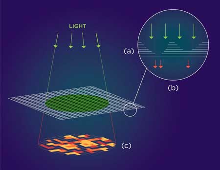
How Atoms-Thin Encryption Can Protect Electronic Hardware
a) At monolayer thickness, this material has the optical properties of a semiconductor that emits light. At multilayer, the properties change and the material doesn’t emit light. (b) Varying the thickness of each layer results in a thin film speckled with randomly occurring regions that alternately emit or block light. (c) Upon exposure to light, this pattern can be translated into a one-of-a-kind authentication key that could secure hardware components at minimal cost. (Image: Althea Labre, NYU Tandon)
„At monolayer thickness, this material has the optical properties of a semiconductor that emits light, but at multilayer, the properties change, and the material no longer emits light. This property is unique to this material,” he said. By tuning the material growth process, the resulting thin film is speckled with randomly occurring regions that alternately emit or do not emit light. When exposed to light, this pattern translates into a one-of-a-kind authentication key that could secure hardware components at minimal cost.
Shahrjerdi said his team was pondering potential applications for what he described as the beautiful random light patterns of MoS2 when he realized it would be highly valuable as a cryptographic primitive.
This represents the first physically unclonable security primitive created using this nanomaterial. Typically embedded in integrated circuits, physically unclonable security primitives protect or authenticate hardware or digital information. They interact with a stimulus – in this case, light – to produce a unique response that can serve as a cryptographic key or means of authentication.
The research team envisions a future in which similar nanomaterial-based security primitives can be inexpensively produced at scale and applied to a chip or other hardware component, much like a postage stamp to a letter. „No metal contacts are required, and production could take place independently of the chip fabrication process,” Shahrjerdi said. „It’s maximum security with minimal investment.”
Source: NYU Tandon School of Engineering

Piezoelectrică – Lăsând plumbul în urmă(Piezoelectrics – Leaving lead behind)

a îmbunătățit considerabil calitatea materialului și performanța filmelor subțiri ale unui material „piezoelectric” fără plumb;Piezoelectricile sunt materiale remarcabile care se deformează la aplicarea unui câmp electric și, invers, produc un curent electric când sunt comprimate. Acestea sunt utilizate în multe aplicații electronice, inclusiv ca servomotoare electromecanice și ca senzori pentru tensiune și accelerație.

Posted: Nov 29, 2017

Piezoelectrics – Leaving lead behind

(Nanowerk News) An advance in fabrication technology has greatly improved the material quality and performance of thin films of a lead-free ‘piezoelectric’ material (Advanced Electronic Materials, „High piezoelectric performance and phase transition in stressed lead-free (1–x)(K,Na)(Sb, Nb)O3-x(Bi,Na,K)ZrO3 thin films”). This development by A*STAR researchers promises to unlock a lead-free alternative to the lead–zircon–titanate (PZT) standard.

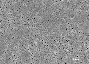
An electron microscopy image of KNN thin film showing
An electron microscopy image of the KNN thin film showing the controlled formation of the crystalline domains responsible for the piezoelectric effect. (Image: A*STAR Institute of Materials Research and Engineering)
Piezoelectrics are remarkable materials that deform on application of an electric field and, conversely, produce an electric current when compressed. They are used in many electronics applications, including as electromechanical actuators and as sensors for strain and acceleration. Thin films of piezoelectric materials are also being integrated into microelectromechanical systems (MEMS) circuits and devices.
For decades, PZT was the piezoelectric material of choice, since it offered the degree of deformation or sensitivity needed for practical applications. However, PZT contains 60 per cent lead — a toxic metal, which although once commonly used in electronics, has been banned.
An alternative material, which is based on a potassium–sodium–niobate composition and is known as KNN, is being used as a replacement for PZT in many bulk applications. Yet thin films of KNN are problematic because they are subject to a breakdown of composition control and the atomic ordering needed to produce the piezoelectric effect.
Now, Kui Yao and colleagues from the A*STAR Institute of Materials Research and Engineering, in collaboration with National University of Singapore researchers, have shown that a solution-based fabrication method using a painstakingly formulated cocktail of chemical agents can produce thin films of KNN with a piezoelectric performance comparable to PZT.
“It has been challenging to achieve excellent piezoelectric properties in KNN-based thin films because the phase conditions needed for the piezoelectric effect depend very sensitively on composition,” explains Yao. “In KNN, it has been difficult to suppress the loss of volatile elements needed for these conditions.”
Yao and his team overcame this problem by adding a blend of chemical stabilizing agents — refined over more than ten years of research — to the precursor solution used to prepare the KNN thin films. The interactions between the volatile alkali ions in solution and the stabilizing agent suppressed volatilization, allowing the compositions of the resulting films to be well controlled.
“With the film composition under control, we were able to study the phase transitions in the material and their dependence on the chemical composition and stress in the KNN-based thin films,” says Yao.
Through laser measurements combined with theoretical analysis from first-principles simulations, the team confirmed that the performance of their piezoelectric films makes them a viable lead-free alternative to PZT.
Source: A*STAR