Un tranzistor realizat din nanofibri de grafen(A transistor made of graphene nanoribbons)

Panglici de grafen, care au doar câteva atomi, așa-numitele nanoribbone de grafen, au proprietăți electrice speciale care le fac candidați promițători pentru nanoelectronica viitorului: în timp ce grafenul – un strat subțire de atom de carbon în formă de fagure – este un material conductiv , poate deveni un semiconductor sub formă de nanoribon. Aceasta înseamnă că are un spațiu suficient de mare pentru energie sau bandă, în care nu pot exista stări de electroni: poate fi pornit și oprit – și astfel poate deveni o componentă cheie a nanotranzistorilor.

Posted: Nov 29, 2017

A transistor made of graphene nanoribbons

(Nanowerk News) Transistors based on carbon nanostructures: what sounds like a futuristic dream could be reality in just a few years’ time. An international research team working with Empa has now succeeded in producing nanotransistors from graphene ribbons that are only a few atoms wide, as reported in the current issue of the trade journal Nature Communications („Short-channel field-effect transistors with 9-atom and 13-atom wide graphene nanoribbons”).

Graphene ribbons that are only a few atoms wide, so-called graphene nanoribbons, have special electrical properties that make them promising candidates for the nanoelectronics of the future: While graphene – a one atom thin, honeycomb-shaped carbon layer – is a conductive material, it can become a semiconductor in the form of nanoribbons. This means that it has a sufficiently large energy or band gap in which no electron states can exist: it can be turned on and off – and thus may become a key component of nanotransistors.
The smallest details in the atomic structure of these graphene bands, however, have massive effects on the size of the energy gap and thus on how well-suited nanoribbons are as components of transistors. On the one hand, the gap depends on the width of the graphene ribbons, while on the other hand it depends on the structure of the edges. Since graphene consists of equilateral carbon hexagons, the border may have a zigzag or a so-called armchair shape, depending on the orientation of the ribbons. While bands with a zigzag edge behave like metals, i.e. they are conductive, they become semiconductors with the armchair edge.
This poses a major challenge for the production of nanoribbons: If the ribbons are cut from a layer of graphene or made by cutting carbon nanotubes, the edges may be irregular and thus the graphene ribbons may not exhibit the desired electrical properties.
Creating a semiconductor with nine atoms
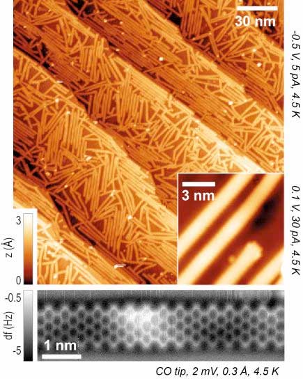
The microscopic ribbons lie criss-crossed on the gold substrate. (Image: Empa)
Empa researchers in collaboration with the Max Planck Institute for Polymer Research in Mainz and the University of California at Berkeley have now succeeded in growing ribbons exactly nine atoms wide with a regular armchair edge from precursor molecules. The specially prepared molecules are evaporated in an ultra-high vacuum for this purpose. After several process steps, they are combined like puzzle pieces on a gold base to form the desired nanoribbons of about one nanometer in width and up to 50 nanometers in length.
These structures, which can only be seen with a scanning tunneling microscope, now have a relatively large and, above all, precisely defined energy gap. This enabled the researchers to go one step further and integrate the graphene ribbons into nanotransistors. Initially, however, the first attempts were not very successful: Measurements showed that the difference in the current flow between the „ON” state (i.e. with applied voltage) and the „OFF” state (without applied voltage) was far too small. The problem was the dielectric layer of silicon oxide, which connects the semiconducting layers to the electrical switch contact. In order to have the desired properties, it needed to be 50 nanometers thick, which in turn influenced the behavior of the electrons.
However, the researchers subsequently succeeded in massively reducing this layer by using hafnium oxide (HfO2) instead of silicon oxide as the dielectric material. The layer is therefore now only 1.5 nanometers thin and the “on”-current is orders of magnitudes higher.
Another problem was the incorporation of graphene ribbons into the transistor. In the future, the ribbons should no longer be located criss-cross on the transistor substrate, but rather aligned exactly along the transistor channel. This would significantly reduce the currently high level of non-functioning nanotransistors.
Source: By Karin Weinmann, Empa

Calculele atomice prezic că încorporarea borului mărește eficiența LED-urilor(Atomistic calculations predict that boron incorporation increases the efficiency of LEDs)

au descoperit că încorporarea elementului bor în materialul InGaN (indiu-galiu nitrida) aglomerat în LED-uri, făcând materialul mai eficient la producerea luminii ( Aplicată Physics Letters , „aliajele BInGaN aproape de zăbrele, potrivite cu GaN pentru LED-urile vizibile de înaltă eficiență de înaltă eficiență” ).

Posted: Nov 28, 2017

Atomistic calculations predict that boron incorporation increases the efficiency of LEDs

(Nanowerk News) High-power white LEDs face the same problem that Michigan Stadium faces on game day — too many people in too small of a space. Of course, there are no people inside of an LED. But there are many electrons that need to avoid each other and minimize their collisions to keep the LED efficiency high.

Using predictive atomistic calculations and high-performance supercomputers at the NERSC computing facility, researchers Logan Williams and Emmanouil Kioupakis at the University of Michigan found that incorporating the element boron into the widely used InGaN (indium-gallium nitride) material can keep electrons from becoming too crowded in LEDs, making the material more efficient at producing light (Applied Physics Letters, „BInGaN alloys nearly lattice-matched to GaN for high-power high-efficiency visible LEDs”).
Crystal structure of a BInGaN alloy
Crystal structure of a BInGaN alloy. (Image: Michael Waters and Logan Williams)
Modern LEDs are made of layers of different semiconductor materials grown on top of one another. The simplest LED has three such layers. One layer is made with extra electrons put into the material. Another layer is made with too few electrons, the empty spaces where electrons would be are called holes. Then there is a thin middle layer sandwiched between the other two that determines what wavelength of light is emitted by the LED.
When an electrical current is applied, the electrons and holes move into the middle layer where they can combine together to produce light. But if we squeeze too many electrons in the middle layer to increase the amount of light coming out of the LED, then the electrons may collide with each other rather than combine with holes to produce light. These collisions convert the electron energy to heat in a process called Auger recombination and lower the efficiency of the LED.
A way around this problem is to make more room in the middle layer for electrons (and holes) to move around. A thicker layer spreads out the electrons over a wider space, making it easier for them to avoid each other and reduce the energy lost to their collisions. But making this middle LED layer thicker isn’t as simple as it sounds.
Because LED semiconductor materials are crystals, the atoms that make them up must be arranged in specific regular distances apart from each other. That regular spacing of atoms in crystals is called the lattice parameter. When crystalline materials are grown in layers on top of one another, their lattice parameters must be similar so that the regular arrangements of atoms match where the materials are joined. Otherwise the material gets deformed to match the layer underneath it. Small deformations aren’t a problem, but if the top material is grown too thick and the deformation becomes too strong then atoms become misaligned so much that they reduce the LED efficiency.
The most popular materials for blue and white LEDs today are InGaN surrounded by layers of GaN. Unfortunately, the lattice parameter of InGaN does not match GaN. This makes growing thicker InGaN layers to reduce electron collisions challenging.
Williams and Kioupakis found that by including boron in this middle InGaN layer, its lattice parameter becomes much more similar to GaN, even becoming exactly the same for some concentrations of boron. In addition, even though an entirely new element is included in the material, the wavelength of light emitted by the BInGaN material is very close to that of InGaN and can be tuned to different colors throughout the visible spectrum. This makes BInGaN suitable to be grown in thicker layers, reducing electron collisions and increasing the efficiency of the visible LEDs.
Although this material is promising to produce more efficient LEDs, it is important that it can be realized in the laboratory. Williams and Kioupakis have also shown that BInGaN could be grown on GaN using the existing growth techniques for InGaN, allowing quick testing and use of this material for LEDs. Still, the primary challenge of applying this work will be to fine tune how best to get boron incorporated into InGaN at sufficiently high amounts. But this research provides an exciting avenue for experimentalists to explore making new LEDs that are powerful, efficient, and affordable at the same time.
Source: By Andrew McAllister and Emmanouil Kioupakis, University of Michigan

Cercetătorii dezvoltă ferestre termocromice foarte eficiente(Researchers develop highly efficient thermochromic windows)

Bazându-se pe astfel de materiale avansate, cum ar fi perovskitul și nanotuburile de carbon cu un singur perete, noua tehnologie răspunde căldurii prin transformarea de la transparent la colorat. Pe măsură ce fereastra se întunecă, aceasta generează energie electrică. Modificarea culorii este condusă de molecule (metilamină) care sunt absorbite în mod reversibil în dispozitiv.

Posted: Nov 28, 2017

Researchers develop highly efficient thermochromic windows

(Nanowerk News) Thermochromic windows capable of converting sunlight into electricity at a high efficiency have been developed by scientists at the U.S. Department of Energy’s National Renewable Energy Laboratory (NREL).

Relying on such advanced materials as perovskites and single-walled carbon nanotubes, the new technology responds to heat by transforming from transparent to tinted. As the window darkens, it generates electricity. The color change is driven by molecules (methylamine) that are reversibly absorbed into the device. When solar energy heats up the device, the molecules are driven out, and the device is darkened. When the sun is not shining, the device is cooled back down, and the molecules re-absorb into the window device, which then appears transparent.
A scientist holds a piece of glass that is split between transparent and opaque
A scientist at NREL holds a piece of glass that is split between transparent and opaque. Lance Wheeler (front) developed a switchable photovoltaic window along with (from left) Nathan Neale, Robert Tenent, Jeffrey Blackburn, Elisa Miller, and David Moore. (Photo by Dennis Schroeder/NREL)
The NREL-developed demonstration device allows an average of 68 percent of light in the visible portion of the solar spectrum to pass through when it’s in a transparent, or bleached, state. When the window changes color—a process that took about 3 minutes of illumination during testing—only 3 percent is allowed through the window. Existing solar window technologies are static, which means they are designed to harness a fraction of the sunlight without sacrificing too much visible light transmission needed for viewing or the comfort of building occupants. “There is a fundamental tradeoff between a good window and a good solar cell,” said Lance Wheeler, a scientist at NREL. “This technology bypasses that. We have a good solar cell when there’s lots of sunshine and we have a good window when there’s not.”
The proof-of-concept paper published in Nature Communications („Switchable photovoltaic windows enabled by reversible photothermal complex dissociation from methylammonium lead iodide”) established a solar power conversion efficiency of 11.3 percent. “There are thermochromic technologies out there but nothing that actually converts that energy into electricity,” Wheeler said. He is the lead author of the paper, “Switchable Photovoltaic Windows Enabled by Reversible Photothermal Complex Dissociation from Methylammonium Lead Iodide.”
His co-authors, all from NREL, are David Moore, Rachelle Ihly, Noah Stanton, Elisa Miller, Robert Tenent, Jeffrey Blackburn, and Nathan Neale.
In testing under 1-sun illumination, the 1-square-centimeter demonstration device cycled through repeated transparent-tinted cycles, but the performance declined over the course of 20 cycles due to restructuring of the switchable layer. Ongoing research is focused on improving cycle stability.
The path to commercialization of the technology was explored last year during a two-month program called Energy I-Corps. Teams of researchers are paired with industry mentors to learn what customers want of the technology and develop viable ways to reach the marketplace. Lance Wheeler and Robert Tenent, the program lead for window technology at NREL and co-author on the paper, teamed up to develop a market strategy for a product they called SwitchGlaze. The effort was funded by the Emerging Technologies program within the Department of Energy’s Building Technologies Office.
Wheeler said the technology could be integrated into vehicles, buildings, and beyond. The electricity generated by the solar cell window could charge batteries to power smartphones or on-board electronics such as fans, rain sensors, and motors that would open or close the windows as programmed.
Source: NREL

Adăugarea de staniu stimulează fotoluminescența nanoparticulelor(Addition of tin boosts nanoparticle’s photoluminescence)

au dezvoltat nanoparticule germaniu cu fotoluminescente imbunatatite, facandu-le potential materiale mai bune pentru celulele solare si sonde de imagistica. Echipa de cercetare a constatat că prin adăugarea de staniu la nucleul de germaniu al nanoparticulei structura sa de zăbrele se potrivește mai bine cu structura zăcământului de acoperire cu sulfură de cadmiu care permite particulelor să absoarbă mai multă lumină

Posted: Nov 28, 2017

Addition of tin boosts nanoparticle’s photoluminescence

(Nanowerk News) Researchers at the U.S. Department of Energy’s Ames Laboratory have developed germanium nanoparticles with improved photoluminescence, making them potentially better materials for solar cells and imaging probes. The research team found that by adding tin to the nanoparticle’s germanium core, its lattice structure better matched the lattice structure of the cadmium-sulfide coating which allows the particles to absorb more light (Chemistry of Materials, „Germanium–Tin/Cadmium Sulfide Core/Shell Nanocrystals with Enhanced Near-Infrared Photoluminescence”).

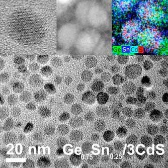
Electron microscopy images of germanium-tin nanoparticles with a cadmium-sulfide coating
Electron microscopy images of germanium-tin nanoparticles with a cadmium-sulfide coating. (Image: Ames Laboratory)
“For a photovoltaic material, obviously absorbing light is the first part and converting that solar energy into electrical energy is the second part,” said Ames Laboratory scientist Emily Smith. “So you want a material that does both efficiently. Germanium has some desirable characteristics for photovoltaic materials, but unfortunately it doesn’t absorb light well.”
Part of the problem is that the outside surface of germanium nanoparticles changes over time, primarily from oxidation. Previous work by Ames Laboratory scientist Javier Vela’s group found that coating nanoparticles—commonly referred to as surface passivation—improved the nanoparticles’ ability to absorb light.
“We aren’t actually measuring absorption,” Smith explained, “we measure the luminescence – the amount light given off after a photon is absorbed. ”
“The fact that germanium doesn’t absorb light well is a simple way of saying it’s an indirect bandgap material,” Smith added, “and we are trying to make a more direct bandgap material, one that absorbs light better.”
According to the research literature, the addition of tin appears to improve germanium’s light absorption properties. However, the Ames Laboratory researchers found that even with adding tin, the nanoparticles still required a surface coating. But they also discovered that the relationship between the atomic structure of surface coating and the core material can further enhance the light absorption.
The specific method used is called Successive Ion Layer Adsorption and Reaction or ‘SILAR’, which was first adapted to group IV colloids several years ago.
„We have been developing the expertise required to grow intricate core/shell and other well defined nanoparticles for many years,” Vela said, “Through our collaboration with Emily Smith’s group, we hope to continue making inroads in our ability to manipulate and direct energy flows at the nanoscale.”
Using transmission electron microscopy imaging and powder X-ray diffraction to study the structural characteristics of the nanoparticles and Raman and photoluminescence spectroscopies to quantify lattice strain and photoluminescence behavior, the group found a correlation between the amount of tin in the core and how well the core’s lattice matched that of the cadmium-sulfide outer shell.
“The atoms are in a very specific location within the nanocrystal core and when you apply the shell around the nanocrystal, the atoms of the shell may not match perfectly with the atoms of the core,” Smith said. “With the germanium only material used previously, the core and shell didn’t match perfectly.”
“When we studied the germanium-tin particles, we proposed that they worked better because the spacing of the atoms better matches the spacing of the atoms we used in the coat layer,” she said. “By doing that, you’re getting a more perfect shell that’s less likely to cause chemical changes to the surface of the nanoparticle core.”
Another potential use for this material, besides photovoltaics, is that in microscopy or imaging, researchers often need to “label” a protein or other feature with a nanoparticle “probe” to make it light up so it is easier to see and study.
Source: Ames Laboratory

Descoperirea celulelor solare deschide o nouă fereastră pentru alimentarea orașelor de mâine(Solar cell discovery opens a new window to powering tomorrow’s cities)

au determinat structura moleculara a electrozilor de lucru cu celule solare in cadrul unui dispozitiv complet asamblat care functioneaza ca o fereastra. Constatarea, publicată în Nanoscale , ajută la avansarea unei tehnologii inteligente de ferestre care ar putea permite orașelor să se apropie de obiectivul de a fi durabile din punct de vedere energetic.
Experimentele au fost efectuate pe celulele solare sensibile la coloranți, care sunt transparente și astfel foarte potrivite pentru utilizarea în sticlă. Încercările de a crea tehnologii inteligente pentru ferestre au fost limitate de numeroase mecanisme moleculare necunoscute între electrozii și electrolitul care se combină pentru a determina modul în care funcționează dispozitivul. a aratat ca anumite ingrediente chimice, unele dintre care pana acum au fost trecute cu vederea, pot influenta in mod clar performanta fotovoltaice a acestor celule solare, Cole a spus.

Posted: Nov 23, 2017

Solar cell discovery opens a new window to powering tomorrow’s cities

(Nanowerk News) Buildings of the future may come equipped with windows that can generate their own electricity, thanks to a finding of a team led by Jacqui Cole, a materials scientist from the University of Cambridge, UK, currently based at the U.S. Department of Energy’s (DOE) Argonne National Laboratory.

For the first time, Cole and colleagues determined the molecular structure of working solar cell electrodes within a fully assembled device that works like a window. The finding, published in Nanoscale, helps advance smart window technology that could enable cities to move closer to the goal of being energy sustainable.
The experiments were performed on dye-sensitized solar cells, which are transparent and thus well-suited for use in glass. Attempts to create smart window technologies have been limited by the many unknown molecular mechanisms between the electrodes and electrolyte that combine to determine how the device operates.
“Most previous studies have modeled the molecular function of these working electrodes without considering the electrolyte ingredients,” Cole said. “Our work shows that these chemical ingredients can clearly influence the performance of solar cells, so we can now use this knowledge to tune the ions to increase photovoltaic efficiency.”
To make the discovery, Cole — the 1851 Royal Commission 2014 Design Fellow — and her colleagues used neutron reflectometry to probe the function and interplay of the electrolyte ingredients with electrodes of the dye-sensitized solar cells. Neutron reflectometry, similar to X-ray reflectometry techniques, allows scientists to measure the structure of thin films with high resolution. But it was the fact that the tests were performed in a window-like system that made for a significant discovery.
“Prior research considered the working electrodes outside the device, so there has been no path to determine how the different device components interact,” Cole said. “Our work signifies a huge leap forward as it’s the world’s first example of applying in situ neutron reflectometry to dye-sensitized solar cells.”
Previous efforts to characterize the dye/titanium dioxide interface in these solar cells have been limited to determining this interfacial structure within an environment exposed to air or in a solvent medium. Because of these constraints, these solar cell environments are essentially artificial with limited relevance for window applications.
With this discovery, however, Cole and colleagues have moved beyond artificial constraints. In doing so, they can better understand how a thin-film electrode containing titanium dioxide, a naturally occurring compound found in paint, sunscreen and food coloring, can have a huge impact on solar cell efficiency.
“Our work has shown that certain chemical ingredients, some of which have so far been overlooked, can clearly influence the photovoltaic performance of these solar cells,” Cole said.
More efficient solar cells like these can move smart window technology closer to the marketplace, said Cole, adding that the science is almost there.
“We just need a modest boost in performance to make these solar cells competitive,” Cole said, “since price-to-performance governs the economics of the solar cell industry. And manufacturing dye-sensitized solar cells is very cheap relative to other solar cell technologies.”
Performance-wise, the cells recently broke a world record with a power conversion efficiency of 14.3 percent using a dye-sensitized electrode featuring two co-sensitized metal-free organic dyes. These dyes “promise cheaper, more environmentally friendly synthetic routes and greater molecular design flexibility than their metal-containing counterparts,” according to the paper.
Source: By Ron Walli, Argonne National Laboratory

Descoperirea celulelor solare deschide o nouă fereastră pentru alimentarea orașelor de mâine(

au determinat structura moleculara a electrozilor de lucru cu celule solare in cadrul unui dispozitiv complet asamblat care functioneaza ca o fereastra.ei pot intelege mai bine cum un electrod subtire care contine dioxid de titan, un compus natural care se gaseste in vopsea, protectie solara si colorarea alimentelor, poate avea un impact imens asupra eficientei celulelor solare.

Posted: Nov 23, 2017

Solar cell discovery opens a new window to powering tomorrow’s cities

(Nanowerk News) Buildings of the future may come equipped with windows that can generate their own electricity, thanks to a finding of a team led by Jacqui Cole, a materials scientist from the University of Cambridge, UK, currently based at the U.S. Department of Energy’s (DOE) Argonne National Laboratory.

For the first time, Cole and colleagues determined the molecular structure of working solar cell electrodes within a fully assembled device that works like a window. The finding, published in Nanoscale, helps advance smart window technology that could enable cities to move closer to the goal of being energy sustainable.
The experiments were performed on dye-sensitized solar cells, which are transparent and thus well-suited for use in glass. Attempts to create smart window technologies have been limited by the many unknown molecular mechanisms between the electrodes and electrolyte that combine to determine how the device operates.
“Most previous studies have modeled the molecular function of these working electrodes without considering the electrolyte ingredients,” Cole said. “Our work shows that these chemical ingredients can clearly influence the performance of solar cells, so we can now use this knowledge to tune the ions to increase photovoltaic efficiency.”
To make the discovery, Cole — the 1851 Royal Commission 2014 Design Fellow — and her colleagues used neutron reflectometry to probe the function and interplay of the electrolyte ingredients with electrodes of the dye-sensitized solar cells. Neutron reflectometry, similar to X-ray reflectometry techniques, allows scientists to measure the structure of thin films with high resolution. But it was the fact that the tests were performed in a window-like system that made for a significant discovery.
“Prior research considered the working electrodes outside the device, so there has been no path to determine how the different device components interact,” Cole said. “Our work signifies a huge leap forward as it’s the world’s first example of applying in situ neutron reflectometry to dye-sensitized solar cells.”
Previous efforts to characterize the dye/titanium dioxide interface in these solar cells have been limited to determining this interfacial structure within an environment exposed to air or in a solvent medium. Because of these constraints, these solar cell environments are essentially artificial with limited relevance for window applications.
With this discovery, however, Cole and colleagues have moved beyond artificial constraints. In doing so, they can better understand how a thin-film electrode containing titanium dioxide, a naturally occurring compound found in paint, sunscreen and food coloring, can have a huge impact on solar cell efficiency.
“Our work has shown that certain chemical ingredients, some of which have so far been overlooked, can clearly influence the photovoltaic performance of these solar cells,” Cole said.
More efficient solar cells like these can move smart window technology closer to the marketplace, said Cole, adding that the science is almost there.
“We just need a modest boost in performance to make these solar cells competitive,” Cole said, “since price-to-performance governs the economics of the solar cell industry. And manufacturing dye-sensitized solar cells is very cheap relative to other solar cell technologies.”
Performance-wise, the cells recently broke a world record with a power conversion efficiency of 14.3 percent using a dye-sensitized electrode featuring two co-sensitized metal-free organic dyes. These dyes “promise cheaper, more environmentally friendly synthetic routes and greater molecular design flexibility than their metal-containing counterparts,” according to the paper.
Source: By Ron Walli, Argonne National Laboratory

Izolatori topologici: este suficientă o singură privire(Topological insulators: one glimpse is enough)

Izolatorii topologici sunt materiale noi cu proprietăți electronice speciale și au un interes fundamental și orientat spre aplicații.Izolatoarele topologice sunt lucruri ciudate. Cea mai mare parte a unui astfel de cristal este izolator și nu poate purta un curent electric, totuși suprafețele aceluiași cristal conduc. Aceste materiale noi au un interes fundamental deosebit, dar sunt, de asemenea, foarte promițătoare pentru o serie de aplicații viitoare în tipuri speciale de electronică și în calculul cuantic și astfel fac obiectul unui efort substanțial de cercetare fizică. Semnificația materialelor topologice a fost subliniată anul trecut prin acordarea Premiului Nobel pentru dezvoltarea teoriilor fundamentale care stabilesc existența și comportamentul materiei topologice.

Posted: Nov 21, 2017

Topological insulators: one glimpse is enough

(Nanowerk News) The Nobel Prize for physics in 2016 was awarded for the theory of topological matter. Topological insulators are new materials with special electronic properties and are of great fundamental and applications-oriented interest. Nevertheless, physicists have wrestled with a ten-year-old puzzle in which the results from the two best methods to probe their electronic states disagree. Researchers from Amsterdam, including two FOM-funded PhD candidates, with collaborators in France, Switzerland and Germany now know exactly why.

he band structure of a topological insulator measured using photoemission
The band structure of a topological insulator measured using photoemission. The dark areas indicate which energies [on the y-axis] go together with which (here inverse) wavelengths [on the x-axis] for the electron waves in the solid. After 20 seconds exposure to the UV light involved in doing a photoemission experiment (right-hand image) the band structure is very different to that after only 1 second exposure (left-hand image). The coloured circles show the position of the Dirac point. (Image: Universiteit van Amsterdam)
Topological insulators are strange stuff. The bulk of such a crystal is insulating and cannot carry an electrical current, yet the surfaces of that same crystal are conducting. These new materials are of great fundamental interest but are also very promising for a number of future applications in special types of electronics and in quantum computation, and so they are the subject of a substantial physics research effort. The significance of topological materials was underlined last year with the award of the Nobel Prize for the development of fundamental theories setting out the existence and behaviour of topological matter.
There are two powerful experimental methods to examine the behaviour of the electrons – the particles that carry electrical current – at the surface of a topological insulator. The first involves sending a current through the system in the presence of a very large magnetic field, and is known as magnetotransport. The second involves the use of an ultraviolet light beam to examine the surface of the crystal. In this case, the energy of a light particle can be absorbed by an electron and in this way those near the surface can escape the crystal and be analysed. Researchers can harness this photo-electric effect to gather valuable information on the electronic properties at the surface of a topological insulator, the place where all the action is. This kind of experiment is called photoemission.
Since more than 10 years, researchers have been baffled as to why these two experiments completely disagree when applied to topological insulators. Now researchers from Amsterdam, including two FOM-funded PhD candidates, together with collaborators in France, Switzerland and Germany recently caught a glimpse of the reasons why. The hypothesis? The very first UV light flash, required to record the photoemission data, itself alters the electronic structure at the surface.
The quantity that describes and explains how electrons in a solid do their stuff is called the band structure. It can be seen as a sort of road network, that maps out the allowed combinations of energy and wavelength the electron-waves can have in the crystal. A slice through such a band structure can be easily displayed as a 2D image like those in the images shown here. This kind of snapshot contains valuable information on the electronic structure of a topological insulator, and in particular the energy location of the crossing-point of the two branches visible in the band structure. This special feature – highlighted with a coloured marker in the images – is called the Dirac point, named for theoretical physicist Paul Dirac whose theory first described electrons like those at the surface of a topological insulator.
Normally, recording a band structure image costs a minute or more. But here the researchers worked hard to bring this down to just a single second, and the left-hand image was the result. The Dirac point (green circle) comes at an energy matching that from magnetotransport data. After only 20 seconds of UV exposure, the red marker in right-hand picture shows that the Dirac point, and the rest of the band structure with it has slid way down in energy, far from the value found in the transport experiments.
It was already known that molecules that stick to the surface of the topological insulator can cause a downward shift of the Dirac point. These new experiments were able to disentangle the effect of the molecules at the surface and that of the UV light, so the researchers could demonstrate that the very first flash of light in fact plays the role of the starter’s pistol, triggering a rapid downward slide of the Dirac point.
These new results are very useful, as photoemission is a very important experiment in the field of topological materials. But do they mean that photoemission is ripe for the rubbish bin? On the contrary! Now that the effect of the UV light is properly understood, protocols could be developed as to how photoemission can be used in the right way in future studies of topological insulators. The photoemission results and the guidelines for improved experimental procedures were published this week in the leading (open access) physics journal, Physical Review X („Trigger of the ubiquitous surface band bending in 3D topological insulators”).
Source: Universiteit van Amsterdam

Proiectarea de aliaje noi de metal folosind nanostructuri construite(Designing new metal alloys using engineered nanostructures)

Un candidat primar pentru acest „material cu care se confruntă plasmă” este tungstenul, datorită punctului său de topire ridicat – cel mai mare dintre metale sub formă pură și randament scăzut de sputtering (numărul de atomi ejectați de ionii energetici din plasmă). Cu toate acestea, stabilitatea tungstenului împotriva recristalizării, rezistența la oxidare, toleranța la radiații pe termen lung și performanța mecanică sunt problematice.tudiază, de asemenea, comportamentul de deformare a „nanolaminatelor” metalice care constau din straturi cristaline și amorfe alternante și încearcă să abordeze limita teoretică a rezistenței aliajelor ușoare de aluminiu prin strategii sinergice de dopaj chimic (adăugând alte elemente într-un material pentru a-și schimba proprietățile).

Posted: Nov 21, 2017

Designing new metal alloys using engineered nanostructures

(Nanowerk News) Materials science is a field that Jason Trelewicz has been interested in since he was a young child, when his father—an engineer—would bring him to work. In the materials lab at his father’s workplace, Trelewicz would use optical microscopes to zoom in on material surfaces, intrigued by all the distinct features he would see as light interacted with different samples.

Jason Trelewicz
Materials scientist Jason Trelewicz in an electron microscopy laboratory at Brookhaven’s Center for Functional Nanomaterials, where he characterizes nanoscale structures in metals mixed with other elements.
Now, Trelewicz—an assistant professor in the College of Engineering and Applied Sciences’ Department of Materials Science and Chemical Engineering with a joint appointment in the Institute for Advanced Computational Science at Stony Brook University and principal investigator of the Engineered Metallic Nanostructures Laboratory—takes advantage of the much higher magnifications of electron microscopes to see tiny nanostructures in fine detail and learn what happens when they are exposed to heat, radiation, and mechanical forces.

In particular, Trelewicz is interested in nanostructured metal alloys (metals mixed with other elements) that incorporate nanometer-sized features into classical materials to enhance their performance. The information collected from electron microscopy studies helps him understand interactions between structural and chemical features at the nanoscale. This understanding can then be employed to tune the properties of materials for use in everything from aerospace and automotive components to consumer electronics and nuclear reactors.

Since 2012, when he arrived at Stony Brook University, Trelewicz has been using the electron microscopes and the high-performance computing (HPC) cluster at the Center for Functional Nanomaterials (CFN)—a U.S. Department of Energy (DOE) Office of Science User Facility at Brookhaven National Laboratory—to perform his research.

“At the time, I was looking for ways to apply my idea of stabilizing nanostructures in metals to an application-oriented problem,” said Trelewicz. “I’ve long been interested in nuclear energy technologies, initially reading about fusion in grade school. The idea of recreating the processes responsible for the energy we receive from the sun here on earth was captivating, and fueled my interest in nuclear energy throughout my entire academic career. Though we are still very far away from a fusion reactor that generates power, a large international team on a project under construction in France called ITER is working to demonstrate a prolonged fusion reaction at a large scale.”

Plasma-facing materials for fusion reactors

Nuclear fusion—the reaction in which atomic nuclei collide—could provide a nearly unlimited supply of safe, clean energy, like that naturally produced by the sun through fusing hydrogen nuclei into helium atoms. Harnessing this carbon-free energy in reactors requires generating and sustaining a plasma, an ionized gas, at the very high temperatures at which fusion occurs (about six times hotter than the sun’s core) while confining it using magnetic fields. Of the many challenges currently facing fusion reactor demonstrations, one of particular interest to Trelewicz is creating viable materials to build a reactor.
“The formidable materials challenges for fusion are where I saw an opportunity for my research—developing materials that can survive inside the fusion reactor, where the plasma will generate high heat fluxes, high thermal stresses, and high particle and neutron fluxes,” said Trelewicz. “The operational conditions in this environment are among the harshest in which one could expect a material to function.”
A primary candidate for such “plasma-facing material” is tungsten, because of its high melting point—the highest one among metals in pure form—and low sputtering yield (number of atoms ejected by energetic ions from the plasma). However, tungsten’s stability against recrystallization, oxidation resistance, long-term radiation tolerance, and mechanical performance are problematic.
Trelewicz thinks that designing tungsten alloys with precisely tailored nanostructures could be a way to overcome these problems. In August, he received a $750,000 five-year award from the DOE’s Early Career Research Program to develop stable nanocrystalline tungsten alloys that can withstand the demanding environment of a fusion reactor. His research is combining simulations that model atomic interactions and experiments involving real-time ion irradiation exposure and mechanical testing to understand the fundamental mechanisms responsible for the alloys’ thermal stability, radiation tolerance and mechanical performance. The insights from this research will inform the design of more resilient alloys for fusion applications.
atomistic simulations to explore the segregation of solute species to grain boundaries (GBs)—interfaces between grains—in nanostructured alloys
Trelewicz and his students perform large-scale atomistic simulations to explore the segregation of solute species to grain boundaries (GBs)—interfaces between grains—in nanostructured alloys, as shown here for an aluminum-magnesium (Al-Mg) system, and its implications for the governing deformation mechanisms. They are using the insights gained through these simulations to design lightweight alloys with theoretical strengths. (Image: Jason Trelewicz )
In addition to the computational resources they use at their home institution, Trelewicz and his lab group are using the HPC cluster at the CFN—and those at other DOE facilities, such as Titan at Oak Ridge Leadership Computing Facility (a DOE Office of Science User Facility at Oak Ridge National Laboratory)—to conduct large-scale atomistic simulations as part of the project.
“The length scales of the structures we want to design into our materials are on the order of a few nanometers to 100 nanometers, and a single simulation can involve up to 10 million atoms,” said Trelewicz. “Using HPC clusters, we can build a system atom-by-atom, representative of the structure we would like to explore experimentally, and run simulations to study the response of that system under various external stimuli. For example, we can fire a high-energy atom into the system and watch what happens to the material and how it evolves, hundreds or thousands of times. Once damage has accumulated in the structure, we can simulate thermal and mechanical forces to understand how defect structure impacts other behavior.”
These simulations inform the structures and chemistries of experimental alloys, which Trelewicz and his students fabricate at Stony Brook University through high-energy milling. To characterize the nanoscale structure and chemical distribution of the engineered alloys, they extensively use the microscopy facilities at the CFN—including scanning electron microscopes, transmission electron microscopes, and scanning transmission electron microscopes. Imaging is conducted at high resolution and often combined with heating within the microscope to examine in real time how the structures evolve with temperature. Experiments are also conducted at other DOE national labs, such as Sandia through collaboration with materials scientist Khalid Hattar of the Ion Beam Laboratory. Here, students in Trelewicz’s research group simultaneously irradiate the engineered alloys with an ion beam and image them with an electron microscope over the course of many days.
“Though this damage does not compare to what the material would experience in a reactor, it provides a starting point to evaluate whether or not the engineered material could indeed address some of the limitations of tungsten for fusion applications,” said Trelewicz.
Electron microscopy at the CFN has played a key role in an exciting discovery that Trelewicz’s students recently made: an unexpected metastable-to-stable phase transition in thin films of nanostructured tungsten. This phase transition drives an abnormal „grain” growth process in which some crystalline nanostructure features grow very dramatically at the expense of others. When the students added chromium and titanium to tungsten, this metastable phase was completely eliminated, in turn enhancing the thermal stability of the material.
“One of the great aspects of having both experimental and computational components to our research is that when we learn new things from our experiments, we can go back and tailor the simulations to more accurately reflect the actual materials,” said Trelewicz.

Other projects in Trelewicz’s research group

The research with tungsten is only one of many projects ongoing in the Engineered Metallic Nanostructures Laboratory.
“All of our projects fall under the umbrella of developing new metal alloys with enhanced and/or multifunctional properties,” said Trelewicz. “We are looking at different strategies to optimize material performance by collectively tailoring chemistry and microstructure in our materials. Much of the science lies in understanding the nanoscale mechanisms that govern the properties we measure at the macroscale.”
Through a National Science Foundation CAREER (Faculty Early Career Development Program) award, Trelewicz and his research group are exploring another class of high-strength alloys—amorphous metals, or “metallic glasses,” which are metals that have a disordered atomic structure akin to glass. Compared to everyday metals, metallic glasses are often inherently higher strength but usually very brittle, and it is difficult to make them in large parts such as bulk sheets. Trelewicz’s team is designing interfaces and engineering them into the metallic glasses—initially iron-based and later zirconium-based ones—to enhance the toughness of the materials, and exploring additive manufacturing processes to enable sheet-metal production. They will use the Nanofabrication Facility at the CFN to fabricate thin films of these interface-engineered metallic glasses for in situ analysis using electron microscopy techniques.
In a similar project, they are seeking to understand how introducing a crystalline phase into a zirconium-based amorphous alloy to form a metallic glass matrix composite (composed of both amorphous and crystalline phases) augments the deformation process relative to that of regular metallic glasses. Metallic glasses usually fail catastrophically because strain becomes localized into shear bands. Introducing crystalline regions in the metallic glasses could inhibit the process by which strain localizes in the material. They have already demonstrated that the presence of the crystalline phase fundamentally alters the mechanism through which the shear bands form.
Trelewicz and his group are also exploring the deformation behavior of metallic “nanolaminates” that consist of alternating crystalline and amorphous layers, and are trying to approach the theoretical limit of strength in lightweight aluminum alloys through synergistic chemical doping strategies (adding other elements to a material to change its properties).
“We leverage resources of the CFN for every project ongoing in my research group,” said Trelewicz. “We extensively use the electron microscopy facilities to look at material micro- and nanostructure, very often at how interfaces are coupled with compositional inhomogeneities—information that helps us stabilize and design interfacial networks in nanostructured metal alloys. Computational modeling and simulation enabled by the HPC clusters at the CFN informs what we do in our experiments.”
Beyond his work at CFN, Trelewicz collaborates with his departmental colleagues to characterize materials at the National Synchrotron Light Source II—another DOE Office of Science User Facility at Brookhaven.
“There are various ways to characterize structural and chemical inhomogeneities,” said Trelewicz. “We look at small amounts of material through the electron microscopes at CFN and on more of a bulk level at NSLS-II through techniques such as x-ray diffraction and the micro/nano probe. We combine this local and global information to thoroughly characterize a material and use this information to optimize its properties.”

Future of next-generation materials

When he is not doing research, Trelewicz is typically busy with student outreach. He connects with the technology departments at various schools, providing them with materials engineering design projects. The students not only participate in the engineering aspects of materials design but are also trained on how to use 3D printers and other tools that are critical in today’s society to manufacture products more cost effectively and with better performance.
Going forward, Trelewicz would like to expand his collaborations at the CFN and help establish his research in metallic nanostructures as a core area supported by CFN and, ultimately, DOE, to achieve unprecedented properties in classical materials.
“Being able to learn something new every day, using that knowledge to have an impact on society, and seeing my students fill gaps in our current understanding are what make my career as a professor so rewarding,” said Trelewicz. “With the resources of Stony Brook University, nearby CFN, and other DOE labs, I have an amazing platform to make contributions to the field of materials science and metallurgy.”
Source: Brookhaven National Laboratory

Observarea atomilor care se deplasează în cristale perovskite hibride dezvăluie indicii pentru îmbunătățirea celulelor solare(Watching atoms move in hybrid perovskite crystals reveals clues to improving solar cells)

Utilizând raze X și lasere, cercetătorii au studiat modul în care o nouă clasă promițătoare de materiale cu celule solare, numite perovskite hibride, se comportă la nivel de nanometrie în timpul funcționării. Experimentele lor au arătat că atunci când se aplică tensiune, ionii migrează în interiorul materialului, creând zone care nu mai sunt la fel de eficiente la conversia luminii în energie electrică.cercetătorii au strălucit un laser pe cristale pentru a măsura o proprietate numită fotoluminescență – capacitatea materialului de a emite lumină când este excitată de un laser – în diferite zone ale cristalelor. Un bun material cu celule solare emit foarte bine lumina, deci cu cât este mai mare fotoluminescența, cu atât este mai eficientă celula solară. Zonele cu concentrații mai mari de brom au avut o fotoluminescență mai mare cu 180% decât zonele epuizate de ioni de brom.

Posted: Nov 21, 2017

Watching atoms move in hybrid perovskite crystals reveals clues to improving solar cells

(Nanowerk News) A team of researchers led by the University of California San Diego has for the first time observed nanoscale changes deep inside hybrid perovskite crystals that could offer new insights into developing low-cost, high-efficiency solar cells.

Using X-ray beams and lasers, researchers studied how a new promising class of solar cell materials, called hybrid perovskites, behaves at the nanoscale level during operation. Their experiments revealed that when voltage is applied, ions migrate within the material, creating regions that are no longer as efficient at converting light to electricity.
„Ion migration hurts the performance of the light absorbing material. Limiting it could be a key to improving the quality of these solar cells,” said David Fenning, a professor of nanoengineering and member of the Sustainable Power and Energy Center at UC San Diego.
Perovskite Photoluminescence
The inside back cover image of the Nov. 20, 2017 issue of Advanced Materials illustrates how ion migration in a hybrid perovskite crystal affects solar cell performance in different areas of the crystal. (Image: AMOLF)
The team, led by Fenning, includes researchers from the AMOLF Institute in the Netherlands and Argonne National Laboratory. Researchers published their findings in Advanced Materials („Direct Observation of Halide Migration and its Effect on the Photoluminescence of Methylammonium Lead Bromide Perovskite Single Crystals”).
Hybrid perovskites are crystalline materials made of a mixture of both inorganic and organic ions. They are promising materials for making next-generation solar cells because they are inexpensive to manufacture and are considerably efficient at converting light to electricity.
However, hybrid perovskites are not very stable, which can make them difficult to study. Microscopic techniques typically used to study solar cells often end up damaging the hybrid perovskites or can’t image beyond their surfaces.
Now, a UC San Diego-led team has shown that by using a technique called nanoprobe X-ray fluorescence, they can probe deep into hybrid perovskite materials without destroying them. „This is a new window to peer inside these materials and see precisely what’s going wrong,” Fenning said.
The researchers studied a type of hybrid perovskite called methylammonium lead bromide, which contains negatively charged bromine ions. Like other hybrid perovskites, its crystalline structure contains many vacancies, or missing atoms, which have been suspected to allow ions to move readily within the material when a voltage is applied.
The researchers first performed nanoprobe X-ray fluorescence measurements on the crystals to create high-resolution maps of the atoms inside the material. The maps revealed that when voltage is applied, the bromine ions migrate from negatively charged areas to positively charged areas.
Next, the researchers shined a laser on the crystals to measure a property called photoluminescence – the material’s ability to emit light when excited by a laser – in different areas of the crystals. A good solar cell material emits light very well, so the higher the photoluminescence, the more efficient the solar cell should be. The areas with higher bromine concentrations had up to 180 percent higher photoluminescence than areas depleted of bromine ions.
„We watch the bromine ions migrate within minutes and see that the resulting bromine-rich areas have the potential to become better solar cells while the performance is degraded in bromine-poor areas,” Fenning said. Fenning and his team are now exploring ways to limit bromine migration in methylammonium lead bromide and other hybrid perovskites. Researchers say that one potential option would be growing hybrid perovskite crystals in different conditions to minimize the number of vacancies and limit ion migration in the crystalline structure.
Source: University of California – San Diego

Dezvoltarea „ABC” pentru exploatarea noilor fenomene în interacțiunile ușoare(Developing ‘ABCs’ for exploiting new phenomena in light-matter interactions)

O clasă unică de materiale manipulate de lumină, cunoscute sub denumirea de metamateriale sau materiale structurate, utilizează modele de lungimi de undă puternic interacționate sau elemente cu dimensiuni de lungime de undă. Datorită acestor structuri interne și superficiale complexe, au apărut noi proprietăți, unele dintre ele prezentând un comportament care a dus la rescrierea „legilor” de lungă durată în ceea ce privește modul în care lumina și alte unde electromagnetice (EM) interacționează cu materialele;Aplicațiile specifice includ vizibilitatea nocturnă, reflectarea căldurii și gestionarea în motoarele aeronavelor și reglarea temperaturii electronice pe sateliți în zonele extreme de temperatură și temperatură.

Posted: Nov 20, 2017

Developing ‘ABCs’ for exploiting new phenomena in light-matter interactions

(Nanowerk News) A unique class of engineered light-manipulating materials, known as metamaterials or structured materials, makes use of patterns of strongly interacting wavelength or sub-wavelength-sized elements. Because of these intricate internal and surface structures, new properties have emerged, some exhibiting behavior that has resulted in rewriting long-understood “laws” for how light and other electromagnetic (EM) waves interact with materials. These materials have been opening up new options for controlling EM waves in many technological arenas, among them imaging, thermal control, and frequency conversion. Specific applications include night-vision, heat reflection and management in aircraft engines, and temperature regulation of electronics on satellites in the hot-and-cold extremes of space.

how an engineered material might be able to convert, generate, or harvest electromagnetic fields exploiting interactions
DARPA’s Nascent Light-Matter Interactions (NLM) program aims to develop theory-anchored models that could yield new structures for materials with never-before-seen electromagnetic properties. This artist’s concept depicts an example of how an engineered material might be able to convert, generate, or harvest electromagnetic fields exploiting interactions that could have far-reaching effects in areas such as sensing, thermal control, frequency conversion, and dynamics.
Although researchers have been taking steps toward putting these materials to practical use, they remain puzzled about the optimal structure designs for desired matter-light interactions. They have yet to model the materials in ways that enable predictions about how specific structured materials will behave under different conditions, such as increased illumination intensities. To fill in these knowledge gaps, DARPA today announced the Nascent Light-Matter Interactions (NLM) program, which seeks to finally develop theory-anchored models that can expand the state of the art in already-observed phenomena while pointing to never-before-realized and new functionality.
“Recent advances in our understanding of light-matter interactions have revealed nascent concepts that could yield new materials with properties way beyond anything we have now,” said Mike Fiddy, DARPA program manager. “Through NLM we aim to identify building blocks to better understand the physics of 2-D and 3-D structured materials, which can then lead to a systematic design approach for controlling electromagnetic waves through these materials. The end goal is to equip designers with rigorous predictive models and design tools to answer the currently elusive question: ‘If I want a material with X property, how do I build it?’”
For example, can we open new pathways for designing materials that provide more efficiency in up-conversion or down conversion of frequencies, which could benefit military capabilities such as night vision? “At the moment, the state-of-the-art of these complicated structures is you pump them with one frequency and they’ll emit maybe 10 percent at another frequency, but they require lots of power in the process,” he said. “Can we develop design tools to create materials with 80, 90, or 100 percent efficiency in converting infrared light into visible light that require very little or no power?”
As Fiddy sees it, lessons learned in the NLM program also might help engineers design better materials, for example, that automatically block the frequency of a laser if it’s shined directly into the eye. Another example is managing extremely hot temperatures, such as those found in turbine aircraft engines. New engineered materials could help precisely manage temperatures in critical hot parts of the engine, which in turn could lead to more efficiency, thus reducing fuel and maintenance costs.
“Similarly, on satellites, as they orient toward the sun they can get ‘cooked’ and when they are out of the sun they are very cold,” Fiddy said. “Those big temperature extremes have to be controlled somehow in the satellite’s design. But if there were more efficient ways of radiating away the sun’s heat using structured materials, that would be very valuable. A general approach to solving this problem could be beneficial for keeping computer chips cool while at the same time opening up new ways to harvest electromagnetic energy.”
It could take years to realize such possibilities, Fiddy noted, but he hopes the NLM program will deliver new levels of understanding and modeling tools that could hasten that day. As such, he added, this new program should benefit existing programs, such as EXTREME, which focuses on specific uses for engineered materials.
The NLM program will unfold in three phases. The first will challenge performers to develop a model and show that it can predict new phenomena and serve as a design tool. The second phase will push researchers to test the models’ actual utility for identifying new materials useful for specific applications. The goal for Phase 3 is to identify specific challenge problems and tie selected performers and their respective focus and applications to the operational needs of DoD stakeholders.
DARPA announced a webcast Proposers Day for potential NLM proposers on Nov. 28, 2017. A Special Notice with registration information and other details is available here: https://go.usa.gov/xnWut. A Broad Agency Announcement (BAA) solicitation will be posted on FBO in the near future.
Source: DARPA

Borofenul strălucește singur ca material plasmonic 2-D(Borophene shines alone as 2-D plasmonic material)

Un film cu grosime de atom de bor ar putea fi primul material bidimensional pur, capabil să emită lumină vizibilă și aproape infraroșie prin activarea plasmonilor;Tehnicile actuale de nanostructurare au reușit să reducă în mod semnificativ conductivitatea termică a acestor materiale, îmbunătățind astfel performanțele lor. Un factor de putere ridicat este, de asemenea, necesar pentru generarea eficientă a energiei, însă îmbunătățirea acestuia a fost limitată deoarece necesită creșterea simultană a puterii termice a materialului și a conductivității sale electrice, ceea ce este dificil. Conductivitatea electrică a rămas scăzută datorită impurităților ionizate din material care suprimă mobilitatea electronilor.

Posted: Nov 20, 2017

Borophene shines alone as 2-D plasmonic material

(Nanowerk News) An atom-thick film of boron could be the first pure two-dimensional material able to emit visible and near-infrared light by activating its plasmons, according to Rice University scientists.

That would make the material known as borophene a candidate for plasmonic and photonic devices like biomolecule sensors, waveguides, nanoscale light harvesters and nanoantennas.
borophene
Rice University scientists calculate that the atom-thick film of boron known as borophene could be the first pure two-dimensional material naturally able to emit visible and near-infrared light by activating its plasmons. The Rice team tested models of three polymorphs and found that triangular borophene, at left, was capable of emitting visible light, while the other two reached near-infrared. (Illustration: Sharmila Shirodkar)
Plasmons are collective excitations of electrons that flow across the surface of metals when triggered by an input of energy, like laser light. Significantly, delivering light to a plasmonic material in one color (determined by the light’s frequency) can prompt the emission of light in another color.
Models by Rice theoretical physicist Boris Yakobson and his colleagues predict that borophene would be the first known 2-D material to do so naturally, without modification.
The lab’s simulations are detailed in a paper by Yakobson with lead authors Yuefei Huang, a graduate student, and Sharmila Shirodkar, a postdoctoral researcher, in the Journal of the American Chemical Society („Two-Dimensional Boron Polymorphs for Visible Range Plasmonics: A First-Principles Exploration”).
Boron is a semiconductor in three dimensions but a metal in 2-D form. That prompted the lab to have a look at its potential for plasmonic manipulation.
“This was kind of anticipated, but we had to do careful work to prove and quantify it,” said Yakobson, whose lab often predicts possible materials that experimentalists later make, like borophene or the boron buckyball. With colleagues Evgeni Penev, an assistant research professor at Rice, and alumnus Zhuhua Zhang, he recently published an extensive review of the state of boron research.
In the new study, the researchers used a computational modeling technique called density functional theory to test plasmonic behavior in three types of free-standing borophene. The material’s baseline crystal structure is a grid of triangles — think graphene but with an extra atom in the middle of each hexagon.
The lab studied models of plain borophene and two polymorphs, solids that incorporate more than one crystalline structure that are formed when some of those middle atoms are removed. Their calculations showed triangular borophene had the widest emission frequencies, including visible light, while the other two reached near-infrared.
“We don’t have enough experimental data to determine which mechanisms contribute how much to the losses in these polymorphs, but we anticipate and include scattering of plasmons against defects and excitation of electrons and holes that lead to their damping,” Shirodkar said.
The researchers said their results present the interesting possibility of manipulating data at subdiffraction wavelengths.
“If you have an optical signal with a wavelength that’s larger than an electronic circuit of a few nanometers, there’s a mismatch,” she said. “Now we can use the signal to excite plasmons in the material that pack the same information (carried by the light) into a much smaller space. It gives us a way to squeeze the signal so that it can go into the electronic circuit.”
“It turns out that’s important because, roughly speaking, it can improve the resolution by 100 times, in some cases,” Yakobson said. “Resolution is limited by wavelength. By using plasmons, you can store information or write into a material at a much higher resolution because of the shrinkage of the wavelength. This could have great benefits for data storage.”
Experimentalists have made borophene only in very small amounts so far and lack methods to transfer the material from the surfaces on which its grown, Yakobson said. Still, there’s plenty for theoretical scientists to study and plenty of progress in the labs.
“One should explore other polymorphs and look for the best one,” Yakobson suggested. “Here, we didn’t. We just considered three, because it’s pretty heavy work — but others need to be screened before we know what is achievable.”
Source: By Mike Williams, Rice University