Valsul cuantic al electronilor indică următoarea generație de jetoane(The quantum waltz of electrons hints at the next generation of chips)

Proiectele lor de cercetare, care au fost publicate recent în ACS Nano și în Nature Communications ( „Rezolvarea divizării spinului în banda de conducere a monostratului MoS 2 ” ), confirmă faptul că materiale precum grafen (C), molibdenită (MoS 2 ) și diselenă de wolfram WSe 2 ) oferă, fie singure, fie prin combinarea unor caracteristici ale acestora, noi perspective în domeniul electronicii – perspective care ar putea duce în cele din urmă la chips-uri mai mici care generează mai puțină căldură.

Posted: Dec 05, 2017

The quantum waltz of electrons hints at the next generation of chips

(Nanowerk News) A group of spintronics researchers at EPFL is using new materials to reveal more of the many capabilities of electrons. The field of spintronics seeks to tap the quantum properties of „spin,” the term often used to describe one of the fundamental properties of elementary particles – in this case, electrons. This is among the most cutting-edge areas of research in electronics today.

Researchers working in the Laboratory of Nanoscale Electronics and Structures (LANES), which is run by Professor Andras Kis, were able to quantify these quantum properties for a category of two-dimensional semiconductors called transition metal dichalcogenides, or TMDCs.
Their research projects, which were published recently in ACS Nano and in Nature Communications („Resolving the spin splitting in the conduction band of monolayer MoS2„), confirm that materials like graphene (C), molybdenite (MoS2) and tungsten diselenide (WSe2) offer, either alone or by combining some of their characteristics, new perspectives for the field of electronics – perspectives that could ultimately lead to smaller chips that generate less heat.
„With the methods we’ve recently developed, we’ve shown that it is possible to access the spin in these TMDC materials, quantify it and use it to introduce new functionalities,” says Kis.
This all takes place at an extremely small scale. In order to access these quantum properties, the researchers must work with high quality materials. „If we want to examine certain characteristics of electrons, including their energy, we need to be able to watch them move over relatively long distances without there being too much dispersion or disruption,” explains Kis.

In the form of waves

The researchers’ method allows them to obtain samples of sufficient quality both to observe how electrons move around in the form of waves and to quantify their energy.
But the LANES team was also able to access another quantum property. Spins of electrons and holes in this type of a 2D semiconductor can be in one of two states, which are conventionally described as being oriented upward – spin up – or downward – spin down. Their energy will be slightly different in each of these two states. That’s called spin splitting, and the EPFL researchers have measured it for the first time for electrons in TMDC materials.
In the second publication, the researchers wrote about how they used the spin splitting in a TMDC in order to introduce polarized spin currents in graphene without using a magnetic field.
These discoveries are a step forward for the emerging field of spintronics and make it increasingly likely that a different property of charge carriers – i.e. spin, in addition to the electrical charge – will play a role in tomorrow’s electronic devices.
Source: Ecole Polytechnique Fédérale de Lausanne

Hibridul electrolit mărește supercapacitanța în nanofibrele verticale de grafen(Hybrid electrolyte enhances supercapacitance in vertical graphene nanosheets)

VGN-urile sunt rețele de nanomateriale de carbon 3-D care cresc în rânduri de foi verticale, oferind o suprafață mare pentru o capacitate mai mare de stocare a încărcăturii. De asemenea, numite nanowale de carbon sau nanoflaze de grafen, VGN oferă promisiuni în sistemele de stocare a energiei de mare putere, celulele de combustie, senzorii bio și dispozitivele magnetice, printre altele.

Posted: Dec 05, 2017

Hybrid electrolyte enhances supercapacitance in vertical graphene nanosheets

(Nanowerk News) Supercapacitors can store more energy than and are preferable to batteries because they are able to charge faster, mainly due to the vertical graphene nanosheets (VGNs) that are larger and positioned closer together. VGNs are 3-D networks of carbon nanomaterial that grow in rows of vertical sheets, providing a large surface area for greater charge storage capacity. Also called carbon nanowalls or graphene nanoflakes, VGNs offer promise in high-power energy storage systems, fuel cells, bio sensors and magnetic devices, amongst others.

Using VGNs as the material for supercapacitor electrodes offers advantages due to their intriguing properties such as an interconnected porous nanoarchitecture, excellent conductivity, high electrochemical stability, and its array of nanoelectrodes. Advantages of VGNs can be enhanced depending on how the material is grown, treated and prepared to work with electrolytes.
„Performance of a supercapacitor not only depends on the geometry of electrode material, but also depends on the type of electrolyte and its interaction with the electrode,” said Subrata Ghosh of the Indira Gandhi Centre for Atomic Research at Homi Bhabha National Institute. „To improve the energy density of a device, [electric] potential window enhancement will be one key factor.”
Scanning electron micrograph of vertical graphene nanosheets with different magnifications
(a)–(c) Scanning electron micrograph of vertical graphene nanosheets with different magnifications. (d) Magnified image of single nanosheets after KOH activation, showing nanopore formation. (© AIP)
In a paper published this week in the Journal of Applied Physics („Enhanced supercapacitance of activated vertical graphene nanosheets in hybrid electrolyte”), Ghosh and a team of researchers discovered ways to improve the material’s supercapacitance properties.
According to modeling, VGNs should be able to provide high charge storage capabilities, and the scientific community is trying to unlock the keys to reaching the levels of efficiency that are theoretically available. Needed improvements to be viable include, for instance, greater capacitance per unit of material, greater retention, less internal resistance, and greater electrochemical voltage ranges (operating potential windows).
„Our motivation was to improve VGN performance,” Ghosh said. „We have taken two strategies. One is inventing a novel electrolyte, and another is improving the VGN structure by chemical activation. The combination of both enhances the charge storage performance remarkably.”
The researcher team treated VGNs with potassium hydroxide (KOH) to activate the electrodes and then allowed the treated electrodes to interact with a hybrid electrolyte, testing the formation of the electric double layer at the electrode/electrolyte interface. They also examined the morphology, surface wettability, columbic efficiency and areal capacitance of VGN.
The novel electrolyte they created is a hybrid that combines the advantages of aqueous and organic electrolytes for a novel hybrid organo-aqueous version that works to increase supercapacitor performance of VGNs. Using an organic salt, Tetraethylammonium tetrafluoroborate (TEABF4), in an acidic aqueous solution of sulfuric acid (H2SO4), they created an electrolyte that extended the device’s operating window.
Improvement of VGN architecture was associated with the process of KOH activation, which grafted the oxygen functional group onto the electrode, improved electrode wettability, reduced internal resistance and provided a fivefold improvement in capacitance of the VGNs. The activation approach in the paper can be applied to other supercapacitor devices that are based on nanoarchitecture, Ghosh said.
„Aqueous and organic electrolytes are extensively used, but they have their own advantages and disadvantages,” he said. „Hence the concept of hybrid electrolyte arises.”
Source: American Institute of Physics

Nanowires noi sunt doar câteva atomi grosime(New nanowires are just a few atoms thick)

Materialele bidimensionale – materialele depuse în straturi cu grosimea de numai câteva atomi – promit atât elementele electronice de înaltă performanță, cât și electronice flexibile și transparente, care ar putea fi stratificate pe suprafețele fizice pentru a face computerele omniprezente.
Cel mai cunoscut material 2-D este grafenul, care este o formă de carbon, dar recent cercetătorii au investigat alte materiale 2-D, cum ar fi disulfura de molibden, care au propriile lor avantaje distincte.

Posted: Dec 04, 2017

New nanowires are just a few atoms thick

(Nanowerk News) Two-dimensional materials – materials deposited in layers that are only a few atoms thick – are promising for both high-performance electronics and flexible, transparent electronics that could be layered onto physical surfaces to make computing ubiquitous.

The best-known 2-D material is graphene, which is a form of carbon, but recently researchers have been investigating other 2-D materials, such as molybdenum disulfide, which have their own, distinct advantages.
A slight mismatch between the hexagonal structures of molybdenum disulfide and tungsten diselenide creates a strain
A slight mismatch between the hexagonal structures of molybdenum disulfide and tungsten diselenide creates a strain that can be released by the formation of a „5|7 dislocation,” in which two hexagons collapse to form a pentagon and a heptagon. Reactions with molybdenum disulfide in the environment cause the dislocation to move deeper into the tungsten diselenide, drawing a nanowire of molybdenum disulfide behind it. (Image courtesy of the researchers)
Producing useful electronics, however, requires integrating multiple 2-D materials in the same plane, which is a tough challenge. In 2015, researchers at King Abdullah University in Saudi Arabia developed a technique for depositing molybdenum disulfide (MoS2) next to tungsten diselenide (WSe2), with a very clean junction between the two materials. With a variation of the technique, researchers at Cornell University then found that they could induce long, straight wires of MoS2 – only a few atoms in diameter– to extend into the WSe2, while preserving the clean junction.
The researchers contacted Markus Buehler, the McAfee Professor of Engineering in MIT’s Department of Civil and Environmental Engineering, who specializes in atomic-level models of crack propagation, to see if his group could help explain this strange phenomenon.
In the latest issue of Nature Materials („Sub-nanometre channels embedded in two-dimensional materials”), the King Abdullah, Cornell, and MIT researchers team with colleagues at Academia Sinica, the Taiwanese national research academy, and Texas Tech University to describe both the material deposition method and the mechanism underlying the formation of the MoS2nanowires, which the MIT researchers were able to model computationally.
„The manufacturing of new 2-D materials still remains a challenge,” Buehler says. „The discovery of mechanisms by which certain desired material structures can be created is key to moving these materials toward applications. In this process, the joint work of simulation and experiment is critical to make progress, especially using molecular-level models of materials that enable new design directions.”

Wired up

The ability to create long, thin MoS2 channels in WSe2 could have a number of applications, the researchers say.
„Based on [the materials’] electrical properties and optical properties, people are looking at using MoS2 and WSe2 for solar cells or for water splitting based on sunlight,” says Gang Seob Jung, an MIT graduate student in civil and environmental engineering and a coauthor on the new paper. „Most of the interesting stuff happens at the interface. When you have not just the one interface – if there are many nanowire interfaces – it could improve the efficiency of a solar cell, even if it’s quite random.”
But the theoretical explanation of the molecular mechanism underlying the nanowires’ formation also raises the hope that their formation could be controlled, to enable the assembly of atom-scale electronic components.
„Two-D materials, one of the most promising candidates for future electronics, ultimately need to beat silicon-based devices, which have achieved a few nanometers in size already,” says Yimo Han, a Cornell graduate student in chemistry and first author on the paper. „Two-D materials are the thinnest in the vertical direction but still span a quite large area in the lateral dimensions. We made the thinnest dislocation-free channels in 2-D materials, which is a big step toward subnanometer electronic devices out of 2-D materials.”

Propagating polygons

In a 2-D crystal, both MoS2 and WSe2 naturally arrange themselves into hexagons in which the constituent elements – molybdenum and sulfur or tungsten and selenium – alternate. Together, these hexagons produce a honeycomb pattern.
The Cornell researchers’ fabrication technique preserves this honeycomb pattern across the junction between materials, a rare feat and one that’s very useful for electronics applications. Their technique uses chemical vapor deposition, in which a substrate – in this case, sapphire – is exposed to gases carrying chemicals that react to produce the desired materials.
The natural sizes of the MoS2 and WSe2 hexagons are slightly different, however, so their integration puts a strain on both crystals, particularly near their junction. If a pair of WSe2hexagons right at the MoS2 junction convert into a hexagon matched with a heptagon (a seven-sided polygon), it releases the strain.
This so-called 5|7 dislocation creates a site at which an MoS2 particle can attach itself. The resulting reaction inserts a molybdenum atom into the pentagon, producing a hexagon, and breaks the heptagon open. Sulfur atoms then attach to the heptagon to form another 5|7 dislocation. As this process repeats, the 5|7 dislocation moves deeper into WSe2 territory, with a nanowire extending behind it. The pattern in which the strain on the mismatched hexagons relaxes and recurs ensures that the dislocation progresses along a straight line.
Source: MIT

DOD folosește mașina pentru a învăța să lupte împotriva următoarei pandemii(DOD Employs Machine Learning to Fight the Next Pandemic)

a contactat virusul ebola mortal de la un liliac, un caz care nu a fost confirmat oficial și raportat;Amenințările pandemice, cum ar fi Ebola, Zika și gripa aviară, nu reprezintă doar un pericol pentru sănătatea publică, ci sunt considerate, de asemenea, amenințări la adresa securității naționale

DOD

Studiul confirmă faptul că materialele din cupru au dungi fluctuante care pot fi legate de supraconductivitatea la temperaturi înalte(Study confirms that cuprate materials have fluctuating stripes that may be linked to high-temperature superconductivity)

au aratat ca superconductorii pe baza de cupru sau cupati – prima clasa de materiale gasite sa transporte electricitate fara pierderi la temperaturi relativ ridicate – contin dungi fluctuante de electroni încărcați-vă și rotiți-vă ca pe niște râuri pe pământ dur.
Dungile sunt zone unde electronii se încarcă, creează benzi de încărcare negativă sau aliniază spini pentru a crea benzi de magnetism. Erau cunoscuți anterior ca existenți în superconductori de cupru la temperaturi apropiate de zero absolut, deși în această friguroasă profundă dungile nu s-au mișcat în jurul lor și rolul lor exact în superconductivitate

Posted: Dec 01, 2017

Study confirms that cuprate materials have fluctuating stripes that may be linked to high-temperature superconductivity

(Nanowerk News) Scientists at the Department of Energy’s SLAC National Accelerator Laboratory and Stanford University have shown that copper-based superconductors, or cuprates – the first class of materials found to carry electricity with no loss at relatively high temperatures – contain fluctuating stripes of electron charge and spin that meander like rivulets over rough ground.

The stripes are zones where electrons either pile up, creating bands of negative charge, or align their spins to create bands of magnetism. They were previously known to exist in cuprate superconductors at temperatures near absolute zero, although in this deep chill the stripes did not move around and their exact role in superconductivity – do they boost or squelch it? – has been unclear.
Now the researchers have computationally demonstrated for the first time that these stripes also exist at high temperatures, but they are subtle and fluctuate in a way that could only be discovered through numerical computer simulations of a precision and scale not done before. The scientists described their study in Science („Numerical evidence of fluctuating stripes in the normal state of high-Tc cuprate superconductors”).
text
An animation based on computer simulations shows stripes of electron charge (white atoms) and spin (red and blue atoms) in a copper-based superconducting material. The stripes are zones where electrons either pile up, creating bands of negative charge, or align their spins (arrows) in a particular pattern to create bands of magnetism. A computational study by researchers at SLAC and Stanford shows these stripes are present in a subtle, fluctuating form at high temperatures. The results will help researchers test theories about how stripes may be related to high-temperature superconductivity. (Image: Farrin Abbott/SLAC National Accelerator Laboratory)
“There’s reason to think that stripes of charge and spin may be intimately tied to the emergence of high-temperature superconductivity in these materials, which was discovered 30 years ago but so far is not understood or explained,” said Edwin Huang, a physics graduate student at Stanford and at the Stanford Institute for Materials and Energy Sciences (SIMES) at SLAC.
“This discovery of fluctuating stripes in a realistic computer model will give us a way to test the many theories about how stripes are related to superconductivity,” Huang said. “We think our results will be useful for scientists doing experimental studies of these materials, and they’ll also help develop and refine the computational techniques that go hand in hand with theory and experiments to push the field forward.”
The results also apply to other novel materials, said SIMES Director Thomas Devereaux. “Materials that spontaneously develop this sort of non-uniform structure are quite commonplace, including magnets and ferroelectrics,” he said. “It can even be thought of as a signature of ‘quantum’ materials, whose surprising properties are produced by electrons that cooperate in unexpected ways. Our numerical results demonstrate that this phenomenon can generally be related to strong interactions between electron charges and spin.”

A Mysterious Phenomenon

In conventional electrical conductors, current is transmitted by electrons acting individually. But in superconductors, electrons pair up to transmit current with virtually no loss.
For 75 years after their discovery, all known superconductors operated only at temperatures close to absolute zero, limiting the way they could be used.
That changed in 1986, when scientists discovered that cuprates could superconduct at much higher (although still quite chilly) temperatures. In fact, certain cuprate compounds are superconducting at temperatures higher than 100 kelvins, or minus 173 degrees Celsius, allowing development of superconducting technologies that can be chilled with liquid nitrogen.
But researchers are still far from their goal of finding superconductors that operate at close to room temperature for highly efficient power lines, maglev trains and other applications that could have a profound impact on society. Without a fundamental understanding of how high-temperature superconductors work, progress has been slow.
Computer modeling is a critical tool for achieving that understanding. Models are sets of mathematical equations based on physics that theorists create and continually refine to simulate a material’s behavior using computer algorithms. They check their models against observations and experimental results to make sure they’re on the right track.
In this case, the team modeled electron behavior and interactions in one of a cuprate’s copper oxide layers, which is where the interesting physics happens, said SIMES staff scientist Brian Moritz. The calculations were run on Stanford’s Sherlock supercomputer cluster at SLAC and at the DOE’s National Energy Research Scientific Computing Center in Berkeley.
The results were in good agreement with data from neutron scattering experiments on a variety of cuprates, the scientists said, confirming that their simulations accurately capture the electronic physics of these materials.

A More Accurate Model

This is the first time the high-temperature behavior of cuprates has been simulated with a realistic model that covers a large enough area of the material to see fluctuating stripes, Huang said. This larger scale also makes the calculations more accurate.
“There was a fine balance we needed to strike,” he said. “These are extremely computationally demanding calculations. But if you simulate the behavior of smaller areas, you won’t be able to see any stripes that emerge. That was the primary limitation of previous studies.”
The simulations show that stripes emerge at temperatures up to 600 degrees Celsius and in a wide range of doping conditions, where compounds are added to a material to tweak its electronic behavior, and so they appear to be a universal trait of cuprate superconductors, the researchers said.
“The idea that there are fluctuating stripes in cuprates is not new, but it has been a controversial topic for many years,” Huang said. “What’s new here is that we can support their existence using unbiased computation on a realistic model of these materials.”
One thing the study does not do, he added, is answer the question of whether or how the fluctuating stripes figure into superconductivity: “That is the direction we want to head toward.”
Source: By Glennda Chui, SLAC National Accelerator Laboratory

Graphene nano penseta poate apuca biomolecule individuale(Graphene nano tweezers can grab individual biomolecules)

Graphene, un material fabricat dintr-un singur strat de atomi de carbon, a fost descoperit cu mai mult de un deceniu în urmă și a încântat cercetătorii cu gama sa de proprietăți uimitoare care s-au găsit utilizări în multe aplicații noi, de la microelectronică la celule solare.
Pensetele de grafen, dezvoltate la Universitatea din Minnesota, sunt mult mai eficiente în captarea particulelor în comparație cu alte tehnici folosite în trecut, datorită faptului că grafenul monostrat este un singur atom gros. a realizat penseta de grafen prin crearea unei structuri sandwich în care un material subțire izolant numit dioxid de hafniu este așezat între un metal electrodul pe o parte și grafenul pe cealaltă. Hidroxidul de hafniu este un material utilizat în mod curent în microcipurile avansate de astăzi.

Posted: Dec 01, 2017

Graphene nano tweezers can grab individual biomolecules

(Nanowerk News) Researchers from the University of Minnesota College of Science and Engineering have found yet another remarkable use for the wonder material graphene—tiny electronic “tweezers” that can grab biomolecules floating in water with incredible efficiency. This capability could lead to a revolutionary handheld disease diagnostic system that could be run on a smart phone.

Graphene, a material made of a single layer of carbon atoms, was discovered more than a decade ago and has enthralled researchers with its range of amazing properties that have found uses in many new applications from microelectronics to solar cells.
The graphene tweezers developed at the University of Minnesota are vastly more effective at trapping particles compared to other techniques used in the past due to the fact that monolayer graphene is a single atom thick.
The research study was published in Nature Communications („Graphene-edge dielectrophoretic tweezers for trapping of biomolecules”).
Atomically sharp edges of electrically driven graphene can act as tweezers that rapidly trap biomolecules from the surrounding solution
Atomically sharp edges of electrically driven graphene can act as “tweezers” that rapidly trap biomolecules from the surrounding solution. (Image: In-Ho Lee, University of Minnesota)

The world’s sharpest tweezers

The physical principle of tweezing or trapping nanometer-scale objects, known as dielectrophoresis, has been known for a long time and is typically practiced by using a pair of metal electrodes. From the viewpoint of grabbing molecules, however, metal electrodes are very blunt. They simply lack the “sharpness” to pick up and control nanometer-scale objects.
“Graphene is the thinnest material ever discovered, and it is this property that allows us to make these tweezers so efficient. No other material can come close,” said research team leader Sang-Hyun Oh, a Sanford P. Bordeau Professor in the University of Minnesota’s Department of Electrical and Computer Engineering. “To build efficient electronic tweezers to grab biomolecules, basically we need to create miniaturized lightning rods and concentrate huge amount of electrical flux on the sharp tip. The edges of graphene are the sharpest lightning rods.”
The team also showed that the graphene tweezers could be used for a wide range of physical and biological applications by trapping semiconductor nanocrystals, nanodiamond particles, and even DNA molecules. Normally this type of trapping would require high voltages, restricting it to a laboratory environment, but graphene tweezers can trap small DNA molecules at around 1 Volt, meaning that this could work on portable devices such as mobile phones.
Using the University of Minnesota’s state-of-the-art nanofabrication facilities at the Minnesota Nano Center, electrical and computer engineering Professor Steven Koester’s team made the graphene tweezers by creating a sandwich structure where a thin insulating material call hafnium dioxide is sandwiched between a metal electrode on one side and graphene on the other. Hafnium dioxide is a material that is commonly used in today’s advanced microchips.
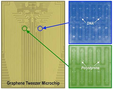
Fluorescence images show DNA molecules and polystyrene nanoparticles trapped on a graphene chip
The University of Minnesota team produced a microchip containing a large array of graphene electronic tweezers. Fluorescence images show DNA molecules and polystyrene nanoparticles trapped on the chip. (Image: Barik et al., University of Minnesota)
“One of the great things about graphene is it is compatible with standard processing tools in the semiconductor industry, which will make it much easier to commercialize these devices in the future,” said Koester, who led the effort to fabricate the graphene devices.
“Since we are the first to demonstrate such low-power trapping of biomolecules using graphene tweezers, more work still needs to be done to determine the theoretical limits for a fully optimized device,” said Avijit Barik, a University of Minnesota electrical and computer engineering graduate student and lead author of the study. “For this initial demonstration, we have used sophisticated laboratory tools such as a fluorescence microscope and electronic instruments. Our ultimate goal is to miniaturize the entire apparatus into a single microchip that is operated by a mobile phone.”

Tweezers that can ‘feel’

Another exciting prospect for this technology that separates graphene tweezers from metal-based devices is that graphene can also “feel” the trapped biomolecules. In other words, the tweezers can be used as biosensors with exquisite sensitivity that can be displayed using simple electronic techniques.
“Graphene is an extremely versatile material,” Koester said. “It makes great transistors and photodetectors, and has the potential for light emission and other novel biosensor devices. By adding the capability to rapidly grab and sense molecules on graphene, we can design an ideal low-power electronics platform for a new type of handheld biosensor.”
Oh agrees that the possibilities are endless.
“Besides graphene, we can utilize a large variety of other two-dimensional materials to build atomically sharp tweezers combined with unusual optical or electronic properties,” said Oh. “It is really exciting to think of atomically sharp tweezers that can be used to trap, sense, and release biomolecules electronically. This could have huge potential for point-of-care diagnostics, which is our ultimate goal for this powerful device.”
Source: University of Minnesota College of Science and Engineering

Metamaterial cu o întorsătură(Metamaterial with a twist)

cercetatorii de la KIT au reusit sa creeze un metamaterial din blocuri de constructii cubice care raspunde fortelor de compresie printr-o rotatie.

Posted: Dec 01, 2017

Metamaterial with a twist

(Nanowerk News) Using 3D printers for the microrange, researchers of KIT have succeeded in creating a metamaterial from cubic building blocks that responds to compression forces by a rotation. Usually, this can only be achieved by transmission using a crankshaft, for instance. The sophisticated design of bars and ring structures and the underlying mathematics are now presented in the latest issue of Science („Three-dimensional mechanical metamaterials with a twist”).

Forces from above are transmitted to the vertical ring structures via bars. The rotation of the rings exerts forces onto the corners of the horizontal planes of the cube
Forces from above are transmitted to the vertical ring structures via bars. The rotation of the rings exerts forces onto the corners of the horizontal planes of the cube. (T. Frenzel/KIT)
“If a force is exerted from above onto a material, the latter deforms in various ways. It may be bulged, compressed, or bent,” says Martin Wegener, Professor of the Institute of Applied Physics and Director of the Institute of Nanotechnology of KIT. “According to the valid rules of mechanics, however, it will not rotate,” he adds. His staff member Tobias Frenzel and colleagues, however, have now succeeded in designing a filigree cubic structure that reacts to loading by a rotation around its axis.
“By means of a computer simulation, we first developed a design with this new mechanical property that has not been described so far,” Frenzel, the first author of the study, explains. “Our calculations revealed that the desired behavior is shown by a complex chiral structure, i.e. a structure that cannot be mapped to its mirror image, similar to the left and the right hand.”
The filigree cubes calculated by Frenzel and his team consist of bars and rings that are connected to each other in a certain pattern. “The arms that connect the ring structures with the corners of the cube move vertically downwards under load. This movement leads to a rotation of the rings,” Frenzel explains. “These rotation movements, in turn, transmit forces to the corners of the horizontal planes of the cube, such that the complete structure starts to twist around its axis.”
Towers of up to 500 chiral cubic structures rotated around their axis under load
Towers of up to 500 chiral cubic structures rotated around their axis under load. (T. Frenzel/KIT)
Towers of up to 500 chiral cubic structures rotated around their axis under load. Achiral structures do not exhibit this behavior. (T. Frenzel/KIT)
Then, the team produced towers of the above cubic structures of variable sizes, strengths, and pieces using a 3D microprinting method established at KIT. The edge length of the cubes ranged from 100 to 500 µm. The researchers built towers of 4 to 500 cubes and 2 mm height. To check their theory, they also built towers of achiral cubes, i.e. cubes that can be mapped to their mirror image.
The scientists found that towers assembled from chiral blocks started to rotate around their axis under the impact of force. “We measured a rotation by up to two degrees per percent of deformation,” Frenzel says. The towers made of achiral cubic structures did not exhibit this rotation. The researchers also found that the stiffness of the towers increased with the number of cubes, although the dimensions of the individual components decreased proportionally.
While towers of up chiral cubic structures rotated around their axis under load, achiral structures do not exhibit this behavior
While towers of up chiral cubic structures rotated around their axis under load, achiral structures do not exhibit this behavior. (T. Frenzel/KIT)
According to Tobias Frenzel, there is still a far way to go to application. Work was inspired by the team’s previous studies of elastic “invisibility cloaks.” These might be used to buffer shock waves of earthquakes or divert them around historic buildings.
Source: Karlsruhe Institute of Technology

Curentul monopole oferă un mod de a controla magneții(Monopole current offers way to control magnets)

au descoperit noi proprietăți magnetice interesante ale unui tip de material cunoscut sub numele de ” cu gheață de spin quantum. ”
Aceste materiale prezintă proprietăți interesante deoarece se comportă ca „magneți frustrați” – sisteme care se pot regla în diferite stări magnetice din cauza geometriei lor speciale. O proprietate importantă a acestor materiale este aceea că au monopoluri virtuale – particule care sunt fie nordice sau sudice, dar nu ca niște magneți tipici, care au în mod invariabil atât un pol de nord cât și un sud limitat împreună.

Posted: Dec 01, 2017

Monopole current offers way to control magnets

(Nanowerk News) In work published in Physical Review Letters („Quantum Spin Ice under a [111] Magnetic Field: From Pyrochlore to Kagome”), scientists from RIKEN in Japan have discovered interesting new magnetic properties of a type of materials known as „quantum spin ice.”

These materials demonstrate interesting properties as they behave as „frustrated magnets”–systems that can settle into various magnetic states because of their special geometry. One important property of these materials is that they have virtual monopoles–particles that are either north or south but not like typical magnets, which invariably have both a north and south pole confined together.
Using numerical simulations, the group showed how a magnetic field could be used to control the properties of north and south poles, which are fractionalized from magnetic moments of electrons, on a frustrated magnet called a quantum spin ice.
The group first proposed a model for quantum spin ice–spin ice based on quantum properties–in 2010 in order to describe the low-energy magnetic properties of magnetic rare-earth pyrochlores–a type of mineral that show interesting physical properties. In 2012, experiments showed that this model was valid. This system includes a quantum spin liquid state where spins–the property of electrons that lead to magnetic properties–are prevented from ordering and freezing by zero-point motion, a type of motion allowed even at zero temperature under quantum mechanics, of their monopoles.
Since monopole charges are subject to a conservation law, the motion of north and south poles directly affects the direction of magnetic moments in the system. In addition, electric charges are not carried by these monopoles, and thus the monopole current is not accompanied by an electric current that would lead to a large energy loss through Joule heat. „Because of this,” says Shigeki Onoda, the leader of the group, „monopole current offers a potentially efficient way of controlling magnets without loss.”
Through this work, the researchers revealed that there are successive transitions from the quantum spin liquid state if a magnetic field is applied in a special direction along which kagome-lattice layers and triangular-lattice layers are stacked one on top of the other.
First, the magnetization of the system rises smoothly to a value two-third of the maximum value in the quantum spin liquid state, and then remains at that level in a finite range of the field strength, which is called the 2/3 magnetization plateau. In this plateau state, the zero-point motion of monopoles are spatially confined and localized, and thus this state cannot host a coherent monopole current.
However, as the strength of the magnetic field is increased, the magnetization of the material eventually begins to rise again and concomitantly, the monopole charges become disproportionate and show a superfluidity. This is a magnetic analogue of a supersolid in helium 4, where the atoms show both a non-uniform spatial distribution and a superfluidity, which supports frictionless and thus dissipationless current, at extremely low temperature. The monopole supersolid phase survives until the magnetization saturates to the maximum value.
According to Onoda, „Our work indicates that the conductivity associated with the monopole current can be substantially controlled by applying a magnetic field to quantum spin ice and that it is possible to host dissipationless monopole current in the monopole supersolid phase. Our findings may also open a novel route to the efficient control of magnetism for a range of potential applications such as memory devices.”
Source: RIKEN

Eliminarea ecologică a biocombustibililor cu nanocoate(Environmentally-friendly removal of biofouling with nanocoatings)

Aceasta înseamnă că vopseaua rezistentă la coroziune durează mai mult timp și mușchii pot fi curățați rapid și ușor”, explică dr. Martina Baum, biolog tehnician de la grupul de lucru al profesorului Rainer Adelung, funcțional Nanomateriale, unde se află ideea inițială acoperirea a apărut acum câțiva ani

Posted: Dec 01, 2017

Environmentally-friendly removal of biofouling with nanocoatings

(Nanowerk News) It is one of the shipping industry’s major problems: marine organisms like barnacles, algae or muscles quickly cover the hulls of ships and damage their paintwork. The phenomenon of so-called „biofouling” increases the ship’s weight and its flow resistance, causing greater fuel consumption and CO2 emissions. In order to avoid this growth, protective paints are mainly used around the world which contain and release pollutants.

A research team at Kiel University and the Phi-Stone AG, one of its spin-offs located in Kiel, have closely cooperated to develop an environmentally-friendly coating. This coating makes it harder for marine organisms to grow on the hulls and makes cleaning the ships easier. The new approach has now been awarded an international prize for innovative marine technology and beat competitors from three continents.
barnacles attached to a ship's hull
A major problem for ships: organisms like barnacles attach themselves to their surfaces, cause damage and also increase their fuel consumption. (Image: HP Voiß)
„This project from the field of nanotechnology is a great example of transferring innovation from Schleswig-Holstein, whereby findings from basic research are brought into industrial application. We, as a university, want to solve existing problems using innovative ideas. In order to do so, this requires a working dialogue between science and companies,” stressed Professor Karin Schwarz, Vice President of technology transfer at Kiel University.

Around 40 percent higher fuel consumption due to biofouling

„We estimate that biofouling increases the amount of fuel ships use by up to 40 percent. This costs the world’s transport industry over 150 billion US dollars per year and causes unnecessary environmental pollution,” added Ingo Paulowicz, Board Member of Phi-Stone, a spin-off from Kiel University.
On top of that, cleaning and maintenance increases considerably, in terms of removing the barnacles and other organisms attached to the hulls and repainting. Many of the existing protective paints have already been forbidden due to their massive polluting effects. This includes organotin paints like TBT (tributyltin). Copper-based compounds are expected to be prohibited next year, which will drastically increase the need for environmentally-friendly and long-lasting coatings for ships.

Longer-lasting and more environmentally-friendly

The coating developed in close collaboration by the scientists from Kiel University and Phi-Stone is both environmentally-friendly and long-lasting. The product requires no solvents and does not release any pollutants into the sea – unlike the widespread self-polishing coatings which contain copper. These are gradually removed when the ship moves through the water and continuously release poisonous substances. The smooth surface of the new coating developed in Kiel makes it harder for organisms to attach themselves to the hulls and destroy the paintwork.
„This means that the bio-corrosion-resistant paint lasts longer and barnacles or muscles can be brushed off quickly and easily,” explains Dr Martina Baum, technical biologist from Professor Rainer Adelung’s Functional Nanomaterials working group, which is where the original idea for the coating arose several years ago.
applying a nanocoating to a ship's hull
The new coating has already been successfully tested on ships like the ‘African Forest’. Technical biologist from Kiel University, Dr Martina Baum, applied the test coating herself. (Image: CAU)
Together with her then-doctoral researcher, materials scientist Iris Hölken, Baum investigated the growth-reduction properties of a polymer composite, which was based on polythiourethane (PTU) and specially-formed ceramic particles. They improve the mechanical properties of the coating and the ability of the paint to adhere to the surface of the ship. Together with Phi-Stone AG, they further developed the material and the coating process.
„Every year around the world, 80,000 tonnes of so-called anti-fouling paints are now being used. This costs around 4 billion dollars per annum. Not to mention the cost to the oceans,” says Phi-Stone Board Member Paulowicz, to emphasise the scale of environmentally-friendly alternatives.

Successful technology transfer through collaboration between Kiel University and Phi-Stone AG

The research team from Kiel University and Phi-Stone AG tested the new product with companies based in Schleswig-Holstein, initially on ships in the water tanks at the GEOMAR Helmholtz Centre for Ocean Research Kiel.
„These tests went very well,” said Baum. „We were able to determine significantly less growth after two years on the ‘African Forest’, which travels from Belgium to Gabon in central Africa. This was then easy to clean off with a plain sponge.” Dr Iris Hölken, who has now completed her doctoral studies, is continuing with this topic as the scientific head of the project at Phi-Stone. The company is currently working on developing a spraying technique, with which the coating can be applied easily and over large areas.

International award for innovative marine technology from Kiel

Phi-Stone AG, the spin-off from Kiel University, won the Global Marine Technology Entrepreneurship Competition in November, with its environmentally-friendly coating for ships. A total of 120 teams took part in the qualifying rounds in Paris, London, Shanghai or at the Massachusetts Institute of Technology in Boston.
The German qualifying round took place in Kiel at the end of October: Ingo Paulowicz, Board Member of Phi-Stone, and staff member Haoyi Qiu, who is also completing a doctoral degree at Kiel University, successfully presented their environmentally-friendly coating concept at the GEOMAR Helmholtz Centre for Ocean Research Kiel. In the finals in Qingdao, in China, they beat the strong competitors from three continents.
The competition, which is organised by Shandong University and the city of Qingdao, aims to promote innovative marine technology and open up contacts to the Chinese market. The first prize is 70,000 US dollars and includes additional funding measures on site.
„We are extremely pleased to have won such a major global competition on maritime innovation,” says Paulowicz, who was also a Kiel University graduate. „We definitely want to keep our company in Schleswig-Holstein, but are excited about the extra possibilities that the Chinese market can offer us.”
„It’s great that this idea was developed in exchange with companies and that we were thus able to transfer it from the lab to the ship,” says Professor Rainer Adelung, head of the working group at Kiel University, who is also very pleased about this success. „It is a great achievement for us as a university, but also for the state, if ideas from Schleswig-Holstein are also convincing at the international level in this way.”
Source: Kiel University