Scotând știința fundamentală a senzorilor(Sniffing out the foundational science of sensors)

Acest senzor poate detecta metanul la concentrații mult mai scăzute decât cele actuale.
În viitor, oamenii de știință ar putea să combine diferite materiale 2D în senzori subțiri și versatil. „Frumusețea materialelor 2D este că puteți să strângeți diferitele straturi împreună pentru a crea materiale artificiale”, a declarat Kai Xiao, om de știință ORNL. Aceste materiale artificiale ar putea detecta o varietate de substanțe chimice diferite, în loc de una singură.Acest senzor sa îmbunătățit atât de mult pe tehnologia existentă încât, în 2016, revista R & D 100 a recunoscut-o ca fiind un finalist în R & D 100. Echipa de cercetare lucrează acum cu proiectul Array of Things, o colaborare între Universitatea din Chicago și ANL. Ca parte a efortului de a colecta date în timp real de la sute de senzori din Chicago, echipa Array of Things anticipează utilizarea acestor senzori de metan în viitor.
Proiecte precum „Array of Things” au potențialul de a transforma orașele în rețele de senzori, plasând ochii și nasul digital pe întregul peisaj construit. Dar aceste rețele și tehnologii nu ar fi posibile fără o bază științifică solidă.

Posted: Mar 22, 2018

Sniffing out the foundational science of sensors

(Nanowerk News) The human nose can distinguish among a trillion different combinations of smells. Even so, there are plenty of gases that our noses can’t detect at the level of sensitivity we need. That’s where gaseous sensors come in. While some of the first sensors were animals – like canaries in coal mines – we’ve since replaced them with technologies that can detect miniscule amounts of chemicals in the air.

Just like our own noses, gaseous sensors are essential for safety and comfort. In factories, gaseous sensors can alert managers to chemical leaks or processes running incorrectly. Outside, they measure pollutants, helping cities monitor air quality. In homes, they keep family members safe. Building managers use measurements from humidity and temperature sensors to maximize energy efficiency.
These sensors wouldn’t exist without a fundamental understanding of chemistry and physics. This basic knowledge helps scientists understand how and why sensing materials interact with gaseous chemicals. Many cutting-edge materials have promise for use in sensors, if only scientists can learn how to better produce and control them.
methane sensor
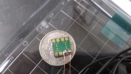
This sensor can detect methane at much lower concentrations than current ones. It relies on nanotechnology developed at the Center for Nanoscale Materials. (Image: Ralu Divan, Argonne National Laboratory)
„Sensors are where materials research meets environmental detection,” said Pete Beckman, a researcher at Department of Energy’s Argonne National Laboratory (ANL).
To set the groundwork for innovation, the DOE Office of Science funds projects and user facilities that support sensors research.

Creating the Materials for Sensing

Like noses, sensors rely on a combination of components to detect and make sense of gases or chemicals in the air. In humans, molecules float up into your nose and bind to special neurons. Neurons then pass the message up to the brain. In sensors, the material inside the sensor acts as a neuron. When that material interacts with a chemical in the air, it may emit light, change its ability to conduct electricity, or shift shape. The materials and electronics around the sensing material communicate that message to the sensor’s „brain,” whether that brain is a computer or a warning signal like a siren.
Developing sensors’ nervous systems and brains is a job for applied science. Fundamental research like the work at the Office of Science’s laboratories sets the foundation for that applied science. In particular, this research is expanding scientists’ understanding of the materials themselves and how to produce them.
Three types of cutting-edge materials offer huge potential for use in sensors: nanoparticles, two-dimensional (2D) materials, and metal-organic frameworks (MOFs). Nanoparticles are miniscule particles that are bigger than atoms, but act fundamentally differently from larger particles of the same substance. 2D materials, like graphene, form sheets only a single atom thick. MOFs are compounds made of metal ions linked together by carbon-based connectors.
All of these materials have humongous surface areas compared to their overall sizes. Because lots of gas molecules can interact with their surfaces, they can be sensitive to tiny amounts of chemicals. In addition, scientists can craft all of these materials into a variety of structures. That customization could allow researchers to create specialty materials to detect a particular chemical.
Zinc Sulfide Nanoparticles
The key to building a better sensor may lie in making its sensing material out of nanoparticles. Unfortunately, it’s challenging to manufacture some of the most promising of those nanoparticles. Sensors for hydrogen and other gases already use the material zinc sulfide. Producing zinc sulfide in nanoparticle form could make it cheaper and more effective. But the current process for producing zinc sulfide nanoparticles involves very high temperatures, pressures, and toxic chemicals.
Scientists at DOE’s Oak Ridge National Laboratory (ORNL) investigated a cheaper, more efficient nanoparticle production process. Researchers supported by both DOE’s Advanced Manufacturing Office and Office of Science found that microbes may offer an alternative path forward („A large-scale technique to produce quantum dots”).
Not just any bacteria will do. Scientists used Thermoanaerobacter, a bacteria that normally lives in extremely hot places with no oxygen. After adding a cheap sugar and chemicals that included zinc and sulfur, the bacteria produced about three-quarters of a pound of zinc sulfide nanoparticles. The process was 90 percent cheaper than current methods.
Growing 2D Materials
2D materials are a special form of nanomaterial that are only a few atoms thick. They have so much surface area compared to their volume that they provide a lot of space for gas molecules to interact and are able to hold a large number of them. But 2D materials act so differently from their normal „bulk” counterparts that scientists don’t have a good grasp on how they grow. Without this understanding, manufacturers can’t consistently produce high-quality versions of them.
To tackle this problem, ORNL scientists explored a better way to grow 2D material gallium selenide (GaSe) (JACS, „Edge-Controlled Growth and Etching of Two-Dimensional GaSe Monolayers”). As they grew the material in a container filled with argon gas, they found that by changing the temperature and flow of the gas, they could switch back and forth between laying down and taking away atoms. But just discovering how to change back and forth between the two states didn’t tell them what was actually happening on the chemical level.
„To visualize what we were doing in the lab, we needed high-resolution, state-of-the-art facilities as well as in-situ diagnosis tools,” said Tolga Aytug, an ORNL scientist. To get that level of precision, the team turned to the Center for Nanophase Materials Sciences, an Office of Science user facility at ORNL. The tools there helped them see how the processes they used to grow the material affected its structure and properties. Based on that information, they refined their methods to get the characteristics they wanted.
In the future, scientists may be able to combine various 2D materials into thin, versatile sensors. „The beauty of 2D materials is that you can stack the different layers together to make some artificial material,” said Kai Xiao, an ORNL scientist. These artificial materials would be able to detect a variety of different chemicals instead of just a single one.
Metal-Organic Frameworks
The metal ions and carbon-based connectors of MOFs form open, cage-like structures. A MOF only a few inches wide has an amazing 2.5 acres of surface area. That provides plenty of space for molecules to interact with.
As a result, MOFs can sense minute levels of chemicals. Scientists control which chemicals they want a MOF to detect by changing the size of its spaces, its shape, or how its parts link to each other.
„For a MOF-based sensor to work, it has to be very selective and very sensitive,” said Praveen Thallapally, a scientist at DOE’s Pacific Northwest National Laboratory (PNNL).
One benefit specific to MOFs is their ability to accommodate new molecules by changing their structures. PNNL scientists found a MOF with a zinc base could capture cobalt and copper. When these metals exited the molecule, the MOF returned to its original structure. This means after a chemical attaches to a MOF and triggers a sensor, someone could reset and reuse the sensor without needing to replace the MOF.
Much of the ongoing research into MOFs focuses on how to discover and build them. MOFs’ traditional starting materials are rigid and difficult to work with. In contrast, polymers (flexible chains of molecules) are easier to control. However, they usually bunch together in dense, disorganized clumps. To draw on the advantages of each, scientists from the University of California, San Diego found a way to use polymers to build MOFs („Novel porous materials made from flexible ‘spaghetti-like’ molecules„). Using both allows researchers to combine MOFs’ consistency and large surface area with polymers’ ease of use. The researchers used the hybrid materials to create thin films, which are typically used in sensors.
The next breakthrough in MOF research may come from computer modeling. Using trial and error to figure out which structure will interact best with a specific chemical could take years and be very expensive. In contrast, powerful computer models using machine learning allow scientists to find just the right material in a few days.
PNNL scientists searching for a MOF that could select between xenon and krypton collaborated with the National Energy Research Scientific Computing Center, an Office of Science user facility at DOE’s Lawrence Berkeley National Laboratory. After searching through more than 120,000 options, their computer model pointed to a calcium-based material that excelled at this task.

Connecting the Nose to the Body

A great sensing material is essential, but it won’t work by itself. Just as a nose needs a body and brain, sensing materials need to be part of a bigger mechanism. Unfortunately, getting these materials to work together within a sensor is often a challenge.
Printing Nanoparticle Ink
„Ink” made of sensing nanoparticles printed onto paper, plastic, rubber, or fabric could allow engineers to create smaller and more flexible sensors.
„Making particles is one thing. But from those particles, making a functional ink is not trivial,” said ORNL scientist Pooran Joshi, in a slight understatement.
One ORNL study (ACS Applied Materials & Interfaces, „Low-Thermal-Budget Photonic Processing of Highly Conductive Cu Interconnects Based on CuO Nanoinks: Potential for Flexible Printed Electronics”) tackled the best way to turn copper-based nanoparticles into high-quality ink. By shining a high-intensity light for only a few millionths of a second, scientists fused the nanoparticles together without melting the surface underneath. When the copper-based nanoparticle ink fused together, it created a printed surface. Researchers then used the printed surface as a component in a temperature sensor.
Combining Nanotubes and Nanocrystals
Scientists know that sensors made of nanotubes and nanocrystals could detect as little as one part per million of a gas – if only they can get these two materials to work together.
Ralu Divan and her team at ANL discovered a way to add nanocrystals of zinc oxide – which is already used in sensors – to carbon nanotubes. Sensors that use the two together could be far more sensitive to methane than current technology. By placing the zinc oxide nanocrystals down atom by atom, they created a thin, consistent layer on top of the nanotubes. With this process, companies can precisely control the zinc oxide’s thickness and coverage.
To examine the bonds between the nanocrystals and nanotubes, the team relied on the Center for Nanoscale Materials, an Office of Science user facility at ANL. „Having everything in one place has saved a lot of time and we were able to move faster than we expected,” said Divan.
As a result, they developed a sensor that could detect much lower concentrations of methane than previous ones. Operators can use it again in seconds instead of minutes or hours.
This sensor improved so much on the existing technology that in 2016, R&D 100 Magazine recognized it as an R&D 100 finalist. The research team is now working with the Array of Things project, a collaboration between the University of Chicago and ANL. As part of the effort to collect real-time data from hundreds of sensors across Chicago, the Array of Things team anticipates using these methane sensors in the future.
Projects such as the Array of Things have the potential to transform cities into networks of sensors, placing digital eyes and noses throughout the built landscape. But these networks and technologies wouldn’t be possible without a solid scientific foundation. Nothing may match the human nose’s versatility, but research the Office of Science is supporting helps fill in the gaps of our biological capabilities.
Source: U.S. Department of Energy, Office of Science

Forțele viitoare să utilizeze inelul compact pentru detectarea amenințărilor chimice(Future Forces to Use Compact Ring for Chemical Threat Detection )

Cererea de senzori compacți, ușori și portabili, care au capacitatea de a se conecta la smartphone-uri și laptopuri sau computere, este în creștere

Future Forces

Frecvența pieptenează substanțele chimice de identificare în regiunea spectrală infraroșie mijlocie(Frequency combs ID chemicals within the mid-infrared spectral region)

Aceste lasere, numite piepteni de frecvență, „acționează ca” conducători „de lumină și au numeroase aplicații – de la transferarea standardelor de timp și îmbunătățirea semnalelor GPS la spectroscopia de precizie”Spectrele noastre multi-banda, controlate de utilizator si ingineri, sunt ideale pentru aplicatii in care se doreste operarea paralela cu multicomb, cum ar fi senzorii de punct pentru monitorizarea in timp real a sintezei chimice in situ, microscopia in apropierea campului si teledetectie „, a spus Nader. „Acești senzori pot crește semnificativ sensibilitatea detectării instrumentelor și tehnicilor, cum ar fi analizoarele de respirație, detectarea cancerului, urmărirea și detectarea explozivilor și monitorizarea sintezei drogurilor”.

Posted: Mar 15, 2018

Frequency combs ID chemicals within the mid-infrared spectral region

(Nanowerk News) Chemical compounds all carry distinctive absorption „fingerprints” within the mid-infrared spectral region of 2 to 12 microns. This offers an opportunity to measure and study chemicals at extremely sensitive levels but researchers lack the tools, like lasers and detectors, needed to operate within the mid-infrared. Recently, there’s been a push to develop new tools to help see and measure these chemical compounds in greater detail.

In a breakthrough, a group of researchers at the National Institute of Standards and Technology developed an on-silicon-chip laser source with outputs that consist of precisely defined and equally spaced optical lines within the mid-infrared spectral region. They report their findings in APL Photonics („Versatile silicon-waveguide supercontinuum for coherent mid-infrared spectroscopy”).
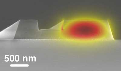
scanning electron micrograph of a fabricated photonic waveguide used in on-chip mid-infrared frequency comb lasers
The scanning electron micrograph of a fabricated photonic waveguide used in on-chip mid-infrared frequency comb lasers. (Image: National Institute of Standards and Technology, Applied Physics Division, Quantum Nanophotonics group)
These lasers, called frequency combs, „act as ‘rulers’ of light and have numerous applications – from transferring time standards and improving GPS signals to precision spectroscopy,” said Nima Nader, a postdoctoral researcher for NIST.
For spectroscopic applications, this type of coherent light source can pass through a sample cell containing unknown gases. These gases absorb some of the light and leave behind fingerprints on very specific comb lines. Researchers can check these lines against a database of gases to identify the specific chemicals present.
Beyond this, the coherent nature of the laser source „enables long-distance propagation of light so chemical samples can be studied remotely, without direct contact,” Nader said. „And since frequency combs are stabilized laser sources, they can detect very low levels of chemicals and enhance the sensitivity of our measurements.”
These sources are fabricated on a compact, silicon-based integrated photonics platform, which enables hundreds of devices – in this case, frequency combs – to be fabricated on a single small-area die.
„Each device is engineered to generate a mid-infrared spectrum of comblike optical lines with tailored spectral shape, bandwidth, and optical power distribution,” Nader said.
These laser sources are „as coherent and low-noise as conventional frequency combs developed prior to our work,” Nader said. „We also reported, for the first time, dual-comb spectroscopy of a gas sample with a mid-infrared frequency comb source that exploits a silicon-photonic platform.”
These developments improve conventional techniques such as Fourier-transform-infrared spectroscopy. A practical, broadband, low-noise mid-infrared frequency comb with moderate power and engineered spectrum may improve the frequency precision, sensitivity, and data acquisition rates of mid-infrared spectroscopy.
„Our user-controlled and engineered multiband spectra are ideal for applications in which parallel multicomb operation is desired – such as point sensors for real-time in situ chemical synthesis monitoring, near-field microscopy, and remote sensing,” Nader said. „These sensors can significantly increase the detection sensitivity of tools and techniques such as breath analyzers, cancer detection, explosives tracking and detection, and drug synthesis monitoring.”
The next step is to push the optical bandwidth of NIST’s frequency combs to longer infrared wavelengths and higher optical powers. „We’re also working to reduce their footprint and power consumption to create compact systems with improved efficiency,” Nader said.
Source: American Institute of Physics

Detectarea cu ochi liber a vaporilor de solvenți(Naked-eye detection of solvent vapor)

a dezvoltat recent un senzor fluorescent eficient pentru vaporii de solvent. Senzorul lor se bazează pe o moleculă ramificată numită dendrimer. Dendrimerul este compus dintr-un nucleu de acceptare a electronilor atașat ramurilor donatoare de electroni. În anumite condiții, dendrimerul se auto-asamblează în fibre care formează un cadru cristalin care conține numeroase pori, ceea ce a ajutat la adsorbția moleculelor de solvent .demonstrează că senzația vizibilă de vapori de solvent poate fi realizată folosind dendrime cristaline cu structuri poroase. Astfel de dendrimeri arată promisiune pentru utilizarea în discriminarea gazelor și a materialelor organice, făcându-le atractive pentru aplicațiile de detectare a mediului.

Posted: Feb 28, 2018

Naked-eye detection of solvent vapor

(Nanowerk News) Sensors are important for detecting contaminants and monitoring environmental conditions. Fluorescent sensors can reveal the presence of a contaminant according to the change of the intensity and/or wavelength of light that they emit. In particular, fluorescent sensors that display changes in emission color are attractive because such changes may be readily observed with the naked eye, making them easy to use.

A research team led by the University of Tsukuba has recently developed an effective fluorescent sensor for solvent vapor. Their sensor is based on a branched molecule called a dendrimer. The dendrimer is composed of an electron-accepting core attached to electron-donating branches. Under certain conditions, the dendrimer self-assembled into fibers that formed a crystalline framework containing numerous pores, which aided adsorption of solvent molecules (Chemical Communications, „A fluorescent microporous crystalline dendrimer discriminates vapour molecules”).
Turn-On PL Sensor for Vapors
Turn-On PL Sensor for Vapors. (Image: University of Tsukuba)
“Slow diffusion of methanol or acetonitrile into chloroform solutions of the dendrimer yielded crystalline microfibers with high porosity,” states Sae Nakajima. “Under other conditions, we obtained amorphous microspheres of the dendrimer that lack pores.”
The research group investigated the crystal structure of the dendrimer by diffraction techniques, finding that the pore volume of the microfiber structure was over 70% of the total crystal volume. The high pore volume of the crystalline dendrimer microfibers greatly increased their gas adsorption capacity over that of the spheres formed under other conditions.
Films of the crystalline dendrimer displayed favorable emission behavior for use in solvent sensing. When the films were exposed to solvent vapor, their emission intensity increased considerably and their emission color quickly changed (within two seconds), reflecting the solvent polarity. This means that a single film could be used to detect numerous types of solvents.
For example, a film appeared blue in a fluorescence microscopy image before solvent exposure and became yellow after introduction of water vapor or green after methanol addition. The film returned to its original color when the solvent vapor was removed, allowing it to be reused.
“Dendrimers typically possess dense amorphous structures. The porous crystalline structure formed by our dendrimer under specific conditions increased its adsorption capacity and sensing ability, revealing the importance of crystalline structure in fluorescent sensing by dendrimers,” says Yohei Yamamoto.
This work demonstrates that the visible sensing of solvent vapor can be realized using crystalline dendrimers with porous structures. Such dendrimers show promise for use in discrimination of gases and organic materials, making them attractive for environmental sensing applications.
Source: University of Tsukuba

Cercetătorii transformă lumina cu susul în jos(Researchers turn light upside down)

Acum, cercetatorii au dezvoltat o astfel de metasurface pentru lumina infrarosie. Se bazează pe nitrura de bor, un material 2D de tip grafen și a fost selectat datorită capacității sale de a manipula lumina infraroșie pe scări extrem de mici, care ar putea fi aplicate pentru dezvoltarea unor senzori chimici miniaturizați sau pentru gestionarea căldurii în dispozitivele optoelectronice nanometrice

Posted: Feb 22, 2018

Researchers turn light upside down

(Nanowerk News) Optical waves propagating away from a point source typically exhibit circular (convex) wavefronts. „Like waves on a water surface when a stone is dropped”, explains Peining Li, EU Marie Sklodowska-Curie fellow at nanoGUNE and first author of the paper. The reason of this circular propagation is that the medium through which light travels is typically homogenous and isotropic i.e. uniform in all directions.

Scientists had already theoretically predicted that specifically structured surfaces can turn the wavefronts of light upside down when it propagates along them.
„On such surfaces, called hyberbolic metasurfaces, the waves emitted from a point source propagate only in certain directions and with open (concave) wavefronts”, explains Javier Alfaro, PhD student at nanoGUNE and co-author of the paper. These unusual waves are called hyperbolic surface polaritons.
Because they propagate only in certain directions, and with wavelengths that are much smaller than that of light in free space or standard waveguides, they could help to miniaturize optical devices for sensing and signal processing.
Now, the researchers developed such a metasurface for infrared light. It is based on boron nitride, a graphene-like 2D material, and was selected because of its capability to manipulate infrared light on extremely small length scales, which could be applied for the development of miniaturized chemical sensors or for heat management in nanoscale optoelectronic devices. On the other hand, the researchers succeeded to directly observe the concave wavefronts with a special optical microscope, which have been elusive so far (Science, „Infrared hyperbolic metasurface based on nanostructured van der Waals materials”).
illustration of waves propagating away from a point-like source
This is an illustration of waves propagating away from a point-like source. Left: Regular wave propagation. Right: Wave propagation on a hyperbolic metasurface. (Image: P. Li, CIC nanoGUNE)
Hyperbolic metasurfaces are challenging to fabricate because an extremely precise structuring on the nanometer scale is required. Irene Dolado, PhD student at nanoGUNE, and Saül Vélez, former postdoctoral researcher at nanoGUNE (now at ETH Zürich) mastered this challenge by electron beam lithography and etching of thin flakes of high-quality boron nitride provided by Kansas State University.
„After several optimization steps, we achieved the required precision and obtained grating structures with gap sizes as small as 25 nm”, Dolado says. „The same fabrication methods can also be applied to other materials, which could pave the way to realize artificial metasurface structures with custom-made optical properties”, adds Saül Vélez.
To see how the waves propagate along the metasurface, the researchers used a state-of the-art infrared nanoimaging technique that was pioneered by the nanoptics group at nanoGUNE. They first placed an infrared gold nanorod onto the metasurface.
„It plays the role of a stone dropped into water”, says Peining Li. The nanorod concentrates incident infrared light into a tiny spot, which launches waves that then propagate along the metasurface. With the help of a so-called scattering-type scanning near-field microscope (s-SNOM) the researchers imaged the waves.
„It was amazing to see the images. They indeed showed the concave curvature of the wavefronts that were propagating away form the gold nanorod, exactly as predicted by theory”, says Rainer Hillenbrand, Ikerbasque Professor at nanoGUNE, who led the work.
The results promise nanostructured 2D materials to become a novel platform for hyberbolic metasurface devices and circuits, and further demonstrate how near-field microscopy can be applied to unveil exotic optical phenomena in anisotropic materials and for verifying new metasurface design principles.
Source: nanoGUNE

Detectarea rapidă a reziduurilor de pesticide cu nanoparticule(Rapid detection of pesticide residue with nanoparticles)

a dezvoltat nanoparticule magnetice acoperite cu polistiren pentru a detecta cantitățile de piretroide din probele de legume cu frunze. Aceste nanoparticule cu miezuri magnetice, atunci când sunt adăugate în scopuri de screening la o probă lichidă din culturi vegetale, pot atrage în mod eficient compușii piretroizi. Nanoparticulele pot fi apoi separate ușor de restul eșantionului prin mijloace magnetice pentru analiză.

Posted: Feb 21, 2018

Rapid detection of pesticide residue with nanoparticles

(Nanowerk News) NUS food scientists have developed polystyrene coated magnetic nanoparticles which allow rapid screening of trace amounts of pesticide residue in vegetable crops (Food Chemistry, „Pyrethroid residue determination in organic and conventional vegetables using liquid-solid extraction coupled with magnetic solid phase extraction based on polystyrene-coated magnetic nanoparticles”).

process involved in using the polystyrene coated magnetic nanoparticles to extract trace pesticide residues from vegetable samples
Figure illustrates the process involved in using the polystyrene coated magnetic nanoparticles (“micro magnets”) to extract trace pesticide residues from vegetable samples. (Image: Yu Xi)
Pesticides are often used in vegetable farming to increase crop yield by controlling agricultural pests that can damage crops. Pyrethroids are a type of synthetic pesticide which are widely applied to crops. However, there are increasing concerns with pyrethroid residue on vegetables as long-term exposure may lead to health issues.
A research team led by Prof YANG Hongshun from the Food Science & Technology Programme at the Department of Chemistry, NUS has developed polystyrene coated magnetic nanoparticles to detect trace amounts of pyrethroids in leafy vegetable samples. These nanoparticles with magnetic cores, when added for screening purposes to a liquid sample of vegetable crops, can effectively attract the pyrethroid compounds. The nanoparticles can then be separated easily from the rest of the sample by magnetic means for analysis.
Transmission electron microscopy image of the polystyrene coated magnetic nanoparticles
Transmission electron microscopy image of the polystyrene coated magnetic nanoparticles. The nanoparticles have a diameter of about 20 nm. (Image: NUS)
Conventional screening methods typically use tedious processes such as filtration and centrifugation to isolate and ascertain the presence of pyrethroids. The approach developed by Prof Yang and his team is a simpler process in which the extraction process can be completed within an hour. Possible applications could include vegetable screening and monitoring programmes to improve food supply safety.
Ms YU Xi, a Ph.D. student working on the project said, “In terms of the accuracy, the recovery rates in our experiments for five kinds of commonly used pyrethroids were greater than 91.6%, which is comparable to conventional methods. This method is also more cost effective as the nanoparticles can be washed and recycled after use.”
“Chemical residue in food products is an important food safety issue for consumers. This method offers a fast and effective way to screen vegetable samples for residue pesticides. It can potentially be adapted for other types of food samples. With small modifications, various food products such as fruits, nuts, meat and vegetable oils can also be tested using this method for possible food hazards,” added Prof Yang.
Source: National University of Singapore

DHS anunță finaliștii în concursul Biothreat-Spotting(DHS Announces Finalists in Biothreat-Spotting Contest )

Un concurs de departamente a avansat cinci sisteme de avertizare timpurie destinate detectării atacurilor biologice;sistem pentru a menține atacurile biologice la distanță

DHS

Camera nouă va identifica IED-urile pentru soldați(New Camera Will Identify IEDs For Soldiers)

Soldații în situații de luptă trebuie să-și scaneze în permanență împrejurimile pentru dispozitivele explozive improvizate (IED), o armă de semnătură a războiului modern de gherilă

New Camera

Cercetătorii au inventat nanoantenele emise de lumină bazate pe perovskite de halogenuri(Researchers invented light-emitting nanoantennas based on halide perovskites)

au dezvoltat noi surse de lumină eficiente nanometrice bazate pe perovskitul halogenurilor. Nanosursele considerate sunt nanoparticule cu lungime subwave, care servesc atât ca emițători, cât și ca nanoantenne și permit intensificarea emisiilor de lumină în mod inerent, fără dispozitive suplimentare. Mai mult decât atât, perovskitul permite reglarea spectrelor de emisie într-un interval vizibil prin modificarea compoziției materialului. Acest lucru face ca noile nanoparticule să fie o platformă promițătoare pentru crearea de dispozitive optoelectronice compacte, cum ar fi chips-uri optice, diode emițătoare de lumină sau senzori.

Posted: Feb 12, 2018

Researchers invented light-emitting nanoantennas based on halide perovskites

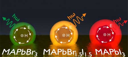
(Nanowerk News) Young scientists from ITMO University developed new effective nanoscale light sources based on halide perovskite. The considered nanosources are subwavelength nanoparticles, which serve both as emitters and nanoantennas and allow enhancing light emission inherently without additional devices. Moreover, perovskite enables tuning emission spectra throughout a visible range by varying the composition of the material. This makes the new nanoparticles a promising platform for creating compact optoelectronic devices such as optical chips, light-emitting diodes, or sensors. The results were published in Nano Letters („Light-Emitting Halide Perovskite Nanoantennas”).

light-emitting nanoantennas based on halide perovskites
The nanoscale light sources and nanoantennas have already found a wide range of applications in several areas, such as ultra compact pixels, optical detection, or telecommunications. However, the fabrication of nanostructure-based devices is rather complicated due to the limited luminescence efficiency of the materials used typically as well as non-directional and relatively weak light emission of single quantum dots or molecules. An even more challenging task is placing a nanoscale light source precisely near a nanoantenna.
A research group from ITMO University managed to combine a nanoantenna and a light source in a single nanoparticle. It can generate, enhance and route emission via excited resonant modes coupled with excitons. „We used hybrid perovskite as a material for such nanoantennas,” says Ekaterina Tiguntseva, the first author of the publication. “Unique features of perovskite enabled us to make nanoantennas from this material. We basically synthesized perovskite films, and then transferred material particles from the film surface to another substrate by means of pulsed laser ablation technique. Compared to alternatives, our method is relatively simple and cost-effective.”
While studying the obtained perovskite nanoparticles, the scientists discovered that their emission can be enhanced if its spectra match with the Mie-resonant mode. „Such resonances were named in honor of Gustav Mie, an outstanding German scientist,” explains George Zograf, Engineer at the Laboratory of Hybrid Nanophotonics and Optoelectronics at ITMO University. “He developed a general theory describing how the light interacts with sphere-like objects smaller than the wavelength. Currently, scientists are particularly interested in Mie-resonances related to dielectric and semiconductor nanoparticles. Perovskites used in our work are also semiconductors with luminescence efficiency much higher than that of many other materials. Our study shows that combination of excitons with the Mie resonance in perovskite nanoparticles makes them efficient light sources at room temperature.”
In addition, the radiation spectrum of the nanoparticles can be changed by varying the anions in the composition of the material. „The structure of the material remains the same, we simply use another component in the synthesis of perovskite films. Therefore, it is not necessary to adjust the method each time. It remains the same, yet the emission color of our nanoparticles changes,” says Ekaterina.
„As far as we know, no one could get subwavelength perovskite nanoantennas with an adjustable emission spectrum before,” adds George. “When we submitted this paper our senior colleagues jokingly demanded that we bake some pastry reflecting the concept of our work in case the article is accepted. As a result, we celebrated the publication of the work with cupcakes in the colors of our nanoparticles’ emission. We adopted this nice tradition from a research group led by Prof. Jeremey Baumberg at the University of Cambridge.”
The scientists are currently continuing the research of light-emitting perovskite nanoantennas using various components for their synthesis. In addition, they are developing new designs of perovskite nanostructures which may improve ultra compact optical and transmission devices.
Source: ITMO University

Un nas mai mare (de) -definire(A higher(er)-definition nose)

MXene este unul dintre cei mai sensibili senzori de gaze raportate vreodată. Această cercetare este semnificativă, deoarece extinde gama de detectare a gazelor comune, permițându-ne să detectăm concentrații foarte scăzute pe care nu am reușit să le detectăm înainte”, a spus Yury Gogotsi, Distinsa Universitate si profesor Bach in Drexel’s College of Engineering, care a fost un autor al studiului, Drexel. Sensibilitatea ridicată a dispozitivului poate fi utilizată pentru detectarea gazelor toxice sau a poluanților găsiți în mediul nostru. „

Posted: Feb 01, 2018

A higher(er)-definition nose

(Nanowerk News) Sensors that sniff out chemicals in the air to warn us about everything from fires to carbon monoxide to drunk drivers to explosive devices hidden in luggage have improved so much that they can even detect diseases on a person’s breath. Researchers from Drexel University and the Korea Advanced Institute of Science and Technology have made a discovery that could make our best „chemical noses” even more sensitive.

In research, recently published in the American Chemical Society journal ACS Nano („Metallic Ti3C2Tx MXene Gas Sensors with Ultrahigh Signal-to-Noise Ratio”), the team describes how a two-dimensional, metallic material called MXene can be used as a highly sensitive detector of gaseous chemicals. The paper suggests that MXene can pick up chemicals, such as ammonia and acetone, which are indicators of ulcers and diabetes, in much lower traces than sensors currently being used in medical diagnostics.
smell detecting sensor
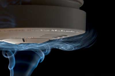
Researchers have discovered that a two-dimensional, metallic material called MXene, which was developed at Drexel, can be used to improve sensors that detect chemicals in the air. (Image: Drexel University)
„MXene is one of the most sensitive gas sensors ever reported. This research is significant because it expands the range for detection of common gases allowing us to detect very low concentrations that we were not able to detect before,” said Yury Gogotsi, PhD, Distinguished University and Bach Professor in Drexel’s College of Engineering, who was a lead Drexel author of the study. „The high sensitivity of the device may be used for detecting toxic gases or pollutants found in our environment.”
Gogotsi’s Nanomaterials Research Group, from Drexel’s Department of Materials Science and Engineering, teamed with Hee-Tae Jung, PhD, a professor at KAIST in Daejeon, South Korea to explore the gas-sensing properties of titanium carbide MXene. The key to its excellent scent-sleuthing capabilities is that MXene is both highly conductive and undergoes a measurable change of electrical conductivity in the presence of the chemical it’s designed to detect – and only when that particular chemical is present.
This discernment is called „signal-to-noise” ratio in the world of chemical sensors and it is used to rank the quality of sensors – picking up more signal and less noise is the goal. The ones in use today – mostly in medical settings to detect chemicals like acetone, ethanol and propanol, or in breathalyzers to detect alcohol – have a signal-to-noise ratio between 3-10, MXene’s is between 170 and 350, depending on the chemical.
„If the material can respond to gases by giving a strong signal, while simultaneously being conductive and achieving low electrical noise, the sensor can detect gases at very low concentrations because the signal-to-noise ratio is high – this is clearly the case with MXene,” Gogotsi said. „MXene can detect gases in the 50-100 parts per billion ranges, which is below the concentration necessary for current sensors to detect diabetes and a number of other health conditions.”
This level of sensitivity could be extremely important for detection of disease. In addition to ulcers and diabetes, breath analysis is currently being developed for early diagnosis of multiple types of cancer, cirrhosis, multiple sclerosis and kidney disease. If the chemical indicators for these diseases can be spotted in lower concentrations they are more likely to be diagnosed and treated at earlier stages.
MXene’s advantage over conventional sensor materials lies in its porous structure and chemical composition. The material is good at both allowing gas molecules to move across its surface and snagging, or adsorbing, certain ones that are chemically attracted to it, showing good selectivity.
Gogotsi’s team has been exploring MXenes since the material’s discovery at Drexel in 2011. The group has been able to create and study more than two dozen different chemical compositions for the material, which means they could be used to create sensors for a very wide variety of gasses.
In the future, Gogotsi suggests, MXene sensors could play an important role in environmental monitoring, energy harvesting and storage, as well as health care.
„The next step to advance this research will be to develop sensor sensitivity to different types of gases and improve the detection selectivity between different gases,” Gogotsi said. „We can also imagine personal sensors that will be in our smart phones or fitness trackers, monitoring body functions and the environment while we work, sleep or exercise, accessible with a tap of a finger. Improving the detection sensitivity with new materials is the first step toward making these devices a reality.”
Source: Drexel University

Software nou pentru prevenirea atacurilor biologice(New Software to Prevent Biological Attacks)

Facilitățile americane de cercetare federală se bazează pe dispozitive conectate la internet pentru a automatiza multe funcții de bază ale clădirilor, cum ar fi ventilația, încălzirea și securitatea, precum și procese mai periculoase, cum ar fi echipamentele de decontaminare și prevenirea microbilor letale de a scăpa de laborator

New Softare to