Un nas mai mare (de) -definire(A higher(er)-definition nose)

MXene este unul dintre cei mai sensibili senzori de gaze raportate vreodată. Această cercetare este semnificativă, deoarece extinde gama de detectare a gazelor comune, permițându-ne să detectăm concentrații foarte scăzute pe care nu am reușit să le detectăm înainte”, a spus Yury Gogotsi, Distinsa Universitate si profesor Bach in Drexel’s College of Engineering, care a fost un autor al studiului, Drexel. Sensibilitatea ridicată a dispozitivului poate fi utilizată pentru detectarea gazelor toxice sau a poluanților găsiți în mediul nostru. „

Posted: Feb 01, 2018

A higher(er)-definition nose

(Nanowerk News) Sensors that sniff out chemicals in the air to warn us about everything from fires to carbon monoxide to drunk drivers to explosive devices hidden in luggage have improved so much that they can even detect diseases on a person’s breath. Researchers from Drexel University and the Korea Advanced Institute of Science and Technology have made a discovery that could make our best „chemical noses” even more sensitive.

In research, recently published in the American Chemical Society journal ACS Nano („Metallic Ti3C2Tx MXene Gas Sensors with Ultrahigh Signal-to-Noise Ratio”), the team describes how a two-dimensional, metallic material called MXene can be used as a highly sensitive detector of gaseous chemicals. The paper suggests that MXene can pick up chemicals, such as ammonia and acetone, which are indicators of ulcers and diabetes, in much lower traces than sensors currently being used in medical diagnostics.
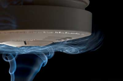
smell detecting sensor
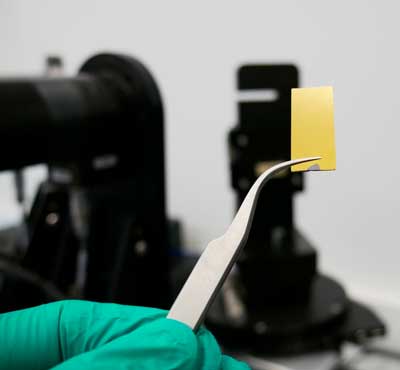
Researchers have discovered that a two-dimensional, metallic material called MXene, which was developed at Drexel, can be used to improve sensors that detect chemicals in the air. (Image: Drexel University)
„MXene is one of the most sensitive gas sensors ever reported. This research is significant because it expands the range for detection of common gases allowing us to detect very low concentrations that we were not able to detect before,” said Yury Gogotsi, PhD, Distinguished University and Bach Professor in Drexel’s College of Engineering, who was a lead Drexel author of the study. „The high sensitivity of the device may be used for detecting toxic gases or pollutants found in our environment.”
Gogotsi’s Nanomaterials Research Group, from Drexel’s Department of Materials Science and Engineering, teamed with Hee-Tae Jung, PhD, a professor at KAIST in Daejeon, South Korea to explore the gas-sensing properties of titanium carbide MXene. The key to its excellent scent-sleuthing capabilities is that MXene is both highly conductive and undergoes a measurable change of electrical conductivity in the presence of the chemical it’s designed to detect – and only when that particular chemical is present.
This discernment is called „signal-to-noise” ratio in the world of chemical sensors and it is used to rank the quality of sensors – picking up more signal and less noise is the goal. The ones in use today – mostly in medical settings to detect chemicals like acetone, ethanol and propanol, or in breathalyzers to detect alcohol – have a signal-to-noise ratio between 3-10, MXene’s is between 170 and 350, depending on the chemical.
„If the material can respond to gases by giving a strong signal, while simultaneously being conductive and achieving low electrical noise, the sensor can detect gases at very low concentrations because the signal-to-noise ratio is high – this is clearly the case with MXene,” Gogotsi said. „MXene can detect gases in the 50-100 parts per billion ranges, which is below the concentration necessary for current sensors to detect diabetes and a number of other health conditions.”
This level of sensitivity could be extremely important for detection of disease. In addition to ulcers and diabetes, breath analysis is currently being developed for early diagnosis of multiple types of cancer, cirrhosis, multiple sclerosis and kidney disease. If the chemical indicators for these diseases can be spotted in lower concentrations they are more likely to be diagnosed and treated at earlier stages.
MXene’s advantage over conventional sensor materials lies in its porous structure and chemical composition. The material is good at both allowing gas molecules to move across its surface and snagging, or adsorbing, certain ones that are chemically attracted to it, showing good selectivity.
Gogotsi’s team has been exploring MXenes since the material’s discovery at Drexel in 2011. The group has been able to create and study more than two dozen different chemical compositions for the material, which means they could be used to create sensors for a very wide variety of gasses.
In the future, Gogotsi suggests, MXene sensors could play an important role in environmental monitoring, energy harvesting and storage, as well as health care.
„The next step to advance this research will be to develop sensor sensitivity to different types of gases and improve the detection selectivity between different gases,” Gogotsi said. „We can also imagine personal sensors that will be in our smart phones or fitness trackers, monitoring body functions and the environment while we work, sleep or exercise, accessible with a tap of a finger. Improving the detection sensitivity with new materials is the first step toward making these devices a reality.”
Source: Drexel University

La cerere, imprimarea 3D a nanostructurilor plasmonice(On-demand 3D-printing of plasmonic nanostructures)

Structurile construite pe scara nanometrilor ar putea construi surse de lumină, senzori și calculatoare noi și îmbunătățite. Oamenii de stiinta au creat un nou mod de a imprima 3-D pe orice material sau forma fara masuratori costisitoare si consumatoare de timpMetoda de imprimare 3D generează nanomateriale personalizate, de la partea de sus în sus, la cerere. Tehnologia deschide calea către fabricarea mascată a arhitecturilor personalizate 1-, 2- și 3-D pe orice formă și material. Materialele pot avea comportamente plasmonice specifice. Oscilațiile oscilante codifică mai multe date decât este posibil cu tehnologiile convenționale. Astfel, acest avans poate accelera apariția unor noi surse de lumină, dispozitive de senzori și tehnologii de stocare ultra-densă a informațiilor.

Posted: Oct 22, 2017

On-demand 3D-printing of plasmonic nanostructures

(Nanowerk News) Structures built on the scale of nanometers could build new and improved light sources, sensors and computers. Scientists created a novel way to 3-D print on virtually any material or shape without costly and time-consuming masking steps (ACS Applied Materials & Interfaces, „Direct-write 3D nanoprinting of plasmonic structures”).

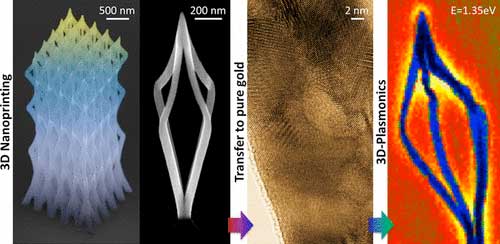
Focused electron beams are used to convert surface-bound molecules made from gold and carbon into the gas phase and deposit them to construct precise 3-D freestanding structures of pure gold
Focused electron beams are used to convert surface-bound molecules made from gold and carbon into the gas phase and deposit them to construct precise 3-D freestanding structures of pure gold. The ultra-sharp features produce free electron oscillations, or quasiparticles called plasmons, with high efficiency. (© ACS)
In a patterned sequence, researchers used a focused electron beam to dissociate surface-bound carbon- and metal-containing molecules and deposit them with precision. The result is a 3-D gold-carbon shape (shown here in a style reminiscent of Gandalf’s staff). They purified these structures in situ (inside the growth reactor) to remove carbon. They tested the resulting freestanding pure-gold architectures for plasmonic behavior—tiny, rapid waves of electron density created when light hits metal.
The 3-D printing approach produces customized, from the bottom up, nanostructures on demand. The technology paves the way to maskless fabrication of custom 1-, 2-, and 3-D architectures on virtually any material and surface shape. The materials can have specific plasmonic behaviors. Plasmonic oscillations encode more data than possible with conventional technologies. Thus, this advance may speed the advent of novel light sources, sensor devices and ultra-dense information storage technologies.
Structures on the scale of nanometers—much smaller than wavelengths of light—may improve transmission of plasmons, or small waves of electron density created when light hits an electron conductor, such as a metal.
To 3-D print nanoscale shapes with controlled properties, researchers integrated design, simulation and experiment. They used pattern sequencing to guide focused electron beams in inducing deposition of organometallic precursor molecules on a surface. Then, they removed residual carbon via in situ purification with water vapor to produce purely metallic freestanding 3-D nanostructures—an advance over previous 2-D nanoprinting with materials that contained significant carbon in addition to the desired metal. The structure that was produced—akin to the outline of up- and down-facing pyramids connected at their bases—demonstrated high plasmonic resonance at branches and tips.
On-demand 3-D printing can take place on virtually any material and surface shape, pushing nanoscale optical, mechanical, magnetic and even multifunctional materials beyond current limits and paving the way to functional plasmonic architectures for next-generation photonic, photovoltaic and data-storage technologies.
Source: Department of Energy, Office of Science

Noile nano-panglici graphene conferă senzorilor o sensibilitate fără precedent(New graphene nano-ribbons lend sensors unprecedented sensitivity)

Pinning panglici de carbon de dimensiuni de ADN la un senzor de gaz poate spori sensibilitatea sale mult mai bine decat orice alt material cunoscut de carbon, spune un nou studiu de la Universitatea din Nebraska-Lincoln.
Echipa a dezvoltat o nouă formă de nano-panglică realizată din grafen, o fagure de 2-D de atomi de carbon. Atunci când cercetătorii au integrat un film al nano-panglicilor în circuitul unui senzor de gaz, acesta a răspuns de aproximativ 100 de ori mai sensibil la molecule decât au făcut senzorii cu cele mai performante materiale pe bază de carbon.

Posted: Oct 20, 2017

New graphene nano-ribbons lend sensors unprecedented sensitivity

(Nanowerk News) Pinning DNA-sized ribbons of carbon to a gas sensor can boost its sensitivity far better than any other known carbon material, says a new study from the University of Nebraska-Lincoln.

The team developed a new form of nano-ribbon made from graphene, a 2-D honeycomb of carbon atoms. When the researchers integrated a film of the nano-ribbons into the circuitry of a gas sensor, it responded about 100 times more sensitively to molecules than did sensors featuring even the best-performing carbon-based materials.
“We previously studied sensors based on other carbon-based materials such as graphene and graphene oxide,” said Alexander Sinitskii, associate professor of chemistry at Nebraska. “In the case of graphene nano-ribbons, we were certain that we would see some sensor response, but we did not expect that it would be that much higher than anything we have seen in the past.”
Reporting their findings in the journal Nature Communications („Laterally extended atomically precise graphene nanoribbons with improved electrical conductivity for efficient gas sensing”), the researchers showed that gas molecules can dramatically alter the electrical resistance of nano-ribbon films. Different gases produced varying resistance signatures, allowing the sensor to distinguish among them.
gas molecules widening the gaps between rows of graphene nano-ribbons
This rendering shows gas molecules widening the gaps between rows of the team’s graphene nano-ribbons. Nebraska’s Alexander Sinitskii and his colleagues have proposed that this phenomenon partly explains how the nano-ribbons grant sensors an unprecedented boost in sensitivity. (© Nature)
“With multiple sensors on a chip, we were able to demonstrate that we can differentiate between molecules that have nearly the same chemical nature,” said Sinitskii, a member of the Nebraska Center for Materials and Nanoscience. “For example, we can tell methanol and ethanol apart. So these sensors based on graphene nano-ribbons can be not only sensitive but also selective.”
Sinitskii and his colleagues suspect that the nano-ribbons’ remarkable performance stems partly from an unusual interaction between the ribbons and gas molecules. Unlike its predecessors, the team’s nano-ribbons — which resemble ordered rows of Charlie Brown’s shirt stripes — stand vertically rather than lying flat on a surface. The team has proposed that gas molecules can nudge these rows apart, effectively lengthening the gaps between nano-ribbons that electrons must jump to conduct electricity.

Enter the (benzene) ring

Graphene, whose 2004 discovery eventually earned a Nobel Prize, boasts unmatched electrical conductivity. But the material’s lack of a band gap — which requires electrons to gain energy before jumping from their near orbits around atoms to an outer “conduction band” that drives conductivity — initially prevented researchers from switching off that conductivity. This, in turn, posed challenges to applying graphene in electronics that require adjusting the material’s conductivity at will.
One potential solution involved trimming sheets of graphene down to nanoscopic ribbons that computer simulations suggested would possess the elusive band gap. This proved difficult to do with the atomic precision needed to preserve the properties that made graphene appealing in the first place, so researchers began fabricating ribbons from the bottom up by strategically snapping together molecules on certain types of solid surfaces. Though the process worked – and the resulting ribbons did have a band gap – it limited researchers to fabricating just a few ribbons at a time.
In 2014, Sinitskii pioneered an approach that could mass-produce nano-ribbons in a liquid solution, a vital step toward scaling up the technology for electronic applications. But the films made from these nano-ribbons were not conductive enough to perform electrical measurements. The team’s newest study adapted the original chemical approach by adding benzene rings — circular molecules with six atoms of both carbon and hydrogen — onto either side of a first-generation nano-ribbon. These rings widened the ribbon, reducing its band gap and enhancing its ability to conduct electricity.
“People do not often think of graphene nano-ribbons as a sensor material,” Sinitskii said. “However, the same (property) that makes the nano-ribbons good for devices such as transistors – the ability to change their conductivity by several orders of magnitude — is also what makes them good for sensors.
“It is possible to design many different kinds of graphene nano-ribbons with very diverse properties. Only a few types have been experimentally demonstrated so far, but there are many interesting theoretical predications about ribbons that are yet to be synthesized by chemists. So it is very likely that new nano-ribbons with even better sensor characteristics or other exciting properties will be developed in the near future.”
Source: By Scott Schrage, University of Nebraska-Lincoln

Oamenii de știință revizuiesc constantele optice ale filmelor de aur ultrascurte(Scientists revisit optical constants of ultrathin gold films)

Filmele metalice cu o grosime de zeci de nanometri sau zeci de miliarde de metru sunt utilizate pe scară largă pentru a produce senzori compacți chimici și biologici, fotodetectoare, celule solare și componente pentru computere optice. Atunci când nanofilmele sunt mai subțiri decât 10 nanometri, ele devin nu doar conductive, ci și flexibile și transparente, care ar putea fi aplicabile într-o varietate de dispozitive moderne.Astfel de filme pot fi folosite în optică și optoelectronică pentru a dezvolta biosenzori compacți cu sensibilitate ridicată, celule solare, fotodetectoare în bandă largă și componente computerizate optoelectronice”. Filmele de aur de acest tip, cu o grosime de aproximativ 40 nanometri, sunt deja utilizate în proiectarea biosenzorilor.

Posted: Oct 17, 2017

Scientists revisit optical constants of ultrathin gold films

(Nanowerk News) Researchers at Moscow Institute of Physics and Technology (MIPT) have conducted highly precise measurements of the optical constants of ultrathin gold films with thicknesses ranging from 20 to 200 billionths of a meter in the optical part of the electromagnetic spectrum. Thin gold films are key components of modern micro- and nanoscale optical and optoelectronic devices. The research findings will be in demand among researchers in the field. The paper was published in the journal Optics Express („Optical constants and structural properties of thin gold films”).

Metal films with a thickness of tens of nanometers, or tens of billionths of a meter, are widely used to produce compact chemical and biological sensors, photodetectors, solar cells, and components for optical computers. When nanofilms are made thinner than 10 nanometers, they become not just conductive but also flexible and transparent, which might be applicable in a variety of modern devices.
gold thin-film
Preparation of a thin gold film sample for spectroscopic ellipsometry measurements. (Image: MIPT)
Gold, which is widely used in nanoscale device development, has proved to be the most suitable metal for the purpose. Such applications require gold in the form of very thin films or nanostructures. To develop and optimize devices, precise data on the properties of such films are necessary. But most of the data used by researchers at present are reported in papers published almost half a century ago.
For instance, one of the most frequently cited articles on the optical constants of gold is „Optical constants of the noble metals” by P.B. Johnson and R.W. Christy, published as early as 1972. The Scopus citation database reveals that the reference constants for gold from this paper have been used in at least 10,000 other publications. To appreciate the significance of this work, it is important to keep in mind that in the 70s, research into the optical properties of thin metal films required a tremendous effort, because the challenging experiments had to be followed by complex calculations and computers were not yet widespread.

Thinner is better

State-of-the-art laboratory equipment and the nearly unlimited computing power available to modern researchers enable more detailed studies of thin metal films. However, it is known that the optical properties of such films – and therefore the efficiency of devices based on them – depend on factors such as film thickness, deposition rate, and the temperature of the substrate used for film deposition.
Accordingly, the MIPT researchers adjusted the initial conditions, namely the deposition rate and the substrate temperature, so as to optimize the optical properties of the film. After that, they conducted the necessary measurements by means of spectroscopic ellipsometry, X-ray diffractometry, electron and atomic force microscopy. The data obtained allowed the MIPT team to study in detail how the properties of thin gold films are related to their structure and average grain size.
The structure of a material affects its physical properties to a large extent, because it is at grain boundaries that conduction electrons are scattered, losing energy – the way a ball in a pinball machine loses its momentum as it runs into obstacles. As it turned out, both optical losses and direct current resistivity are substantially increased, as the thickness of the gold film is reduced to below 80 nanometers.
The authors of the paper provide reference data on the optical constants of gold for a wide range of wavelengths, from 300 to 2,000 nanometers, for films that are 20 to 200 nanometers thick. These findings will be of use to researchers working on various nanophotonic devices and metamaterials.

State-of-the-art technology

To grow thin films, the researchers used a technique called electron beam evaporation, which involves the following steps:: A purified silicon substrate is introduced into a vacuum chamber. Opposite the substrate, a metal sample is positioned. The metal, in this case gold, is then subjected to a beam of electrons accelerated by an electric field. This rapidly heats up the gold causing it to melt and eventually transform into vapor. The evaporated gold atoms are then transported across a region of low pressure from their source and undergo condensation on the substrate to form the thin film.
„Provided that you maintain a high vacuum, heat the metal appropriately, and otherwise follow the procedure, this technique yields films of arbitrary thickness, which is determined by the evaporation time. Moreover, the films are almost perfectly smooth, having a roughness of less than a nanometer,” comments Valentyn Volkov, who heads the Laboratory of Nanooptics and Plasmonics at MIPT. „Such films can be used in optics and optoelectronics to develop high-sensitivity compact biosensors, solar cells, broadband photodetectors, and optoelectronic computer components.” Gold films of this kind with a thickness of about 40 nanometers are already used in biosensor design.
Source: Moscow Institute of Physics and Technology

Nanoantenna arrays putere o nouă generație de senzori bazați pe fluorescență(Nanoantenna arrays power a new generation of fluorescence-based sensors)

au proiectat si testat o serie de matrice nanoantenna plasmonica care ar putea duce la dezvoltarea unei noi generatii de senzori de fluorescenta ultrasensibili si cu costuri reduse care ar putea să fie utilizat pentru a monitoriza calitatea apei.care dezvoltă senzori de fluorescență cuantificați, care vor ajuta la identificarea bacteriilor în câteva minute, nu în câteva zile.

Posted: Oct 16, 2017

Nanoantenna arrays power a new generation of fluorescence-based sensors

(Nanowerk News) Researchers from the Universities of Bristol and Bedfordshire, in collaboration with multinational company ABB, have designed and tested a series of plasmonic nanoantenna arrays that could lead to the development of a new generation of ultrasensitive and low-cost fluorescence sensors that could be used to monitor water quality.

The arrays, designed and tested by Dr Neciah Dorh during his PhD at the University of Bristol, are made from aluminium nanorods fabricated using electron beam lithography by commercial partner Kelvin Nanotechnologies. The nanorods, 50nm wide and 158nm long, are designed to resonantly enhance fluorescence emission from a range of contaminants in water such as diesel or tryptophan.
Nanoantenna Array
SEM images of nanoantenna array and in the inset a magnified view of the array elements. (Image: University of Bristol)
The work, published in Applied Optics („Nanoantenna arrays combining enhancement and beam control for fluorescence-based sensing applications”), shows a six-fold increase in measured fluorescence emission from a dye. The research also shows that by correctly designing the array element spacing, strongly directional fluorescent emission can be obtained which would allow for highly integrated multi-wavelength sensors to be designed.
The work was carried out in Professor Martin Cryan’s research group, which is part of the Photonics Research group in the Department of Electrical and Electronic Engineering.
The project was a collaboration with Dr Andrei Sarua from the School of Physics at Bristol and Dr Tahmina Ajmal from the University of Bedfordshire, who had previously worked on the Aquatest project at Bristol.
Together they developed a prototype low-cost, LED based sensor system, which they plan to develop further into a hand-held field deployable system for performing water quality monitoring.
Martin Cryan, Professor of Applied Electromagnetics and Photonics in the Department of Electrical and Electronic Engineering at the University of Bristol and co-author on the paper, said: „The nanoantenna arrays, which can be fabricated by lower cost production techniques such as nanoimprint lithography, can bring significant sensitivity enhancement so that laboratory quality measurements could be carried out in the field. This would allow for deployment of remote wireless sensor networks for early warning of pollution or continuous monitoring of water quality in sensitive environments.”
Dr Dorh, now a Fellow within Bristol’s QTEC programme, has co-founded a start-up, FluoretiQ, developing quantum enhanced fluorescence sensors which will help identify bacteria within minutes rather than days.
Professor Cryan’s group is developing systems that could combine the power of nanoantennas with quantum enhanced sensors to produce yet further sensitivity enhancements.
Source: University of Bristol

Reglarea fină a materialelor heterociclice cu conținut de fosfor pentru electronica electronică ( Fine tuning phosphorous heterocycle materials for organic electronics )

Oamenii de stiinta de la Institutul de Tehnologie de la Tokyo au produs materiale 1-aril 1,3-difosfaciclobutan-2,4-diil stationar prin arilare directa cu substituenti aromatici bogati in electroni. Această metodă permite reglarea fină a proprietăților electronice ale unor astfel de compuși heterociclii fosforici pentru aplicații care includ fabricarea de senzori electronici organici și fluorură de fluor.ar putea permite detectarea vizuală a existenței HF și ar putea fi utilizată pentru dezvoltarea senzorilor HF.

Posted: May 10, 2016

Fine tuning phosphorous heterocycle materials for organic electronics

(Nanowerk News) Scientists at Tokyo Institute of Technology have produced airstable 1-aryl 1,3-diphosphacyclobutane-2,4-diyl materials by direct arylation with electron rich aromatic substituents. This method enables the fine tuning of the electronic properties of such phosphorous heterocycles compounds for applications including fabrication of organic electronics and hydrogen fluoride sensors (Angew. Chem. Int. Ed., „Access to Air-Stable 1,3-Diphosphacyclobutane-2,4-diyls by an Arylation Reaction with Arynes”).

Materials scientists have a strong interest in the development of methods for the synthesis of so-called ‘open-shell singlet P-heterocyclic’ materials systems for applications in the organic electronics industry including organically based sensors and optoelectronic devices. Here, Shigekazu Ito and colleagues at School of Materials and Chemical Technology, Tokyo Institute of Technology report on a new method for the production of airstable 1-aryl 1,3-diphosphacyclobutane-2,4-diyls— an open-shell singlet P-heterocyclic’ materials system—by direct arylation with electron rich aromatic substituents. This ability to tune the physiochemical nature of the electron-donating 1-aryl 1,3-diphosphacyclobutane-2,4-diyls is expected to find applications including p-type semiconductors and sensors of hydrogen fluoride.
Reversible change of color via the hydrofluorination process
Reversible change of color via the hydrofluorination process.
Background
The Tokyo Tech group have previously reported on a nucleophilic aromatic substitution (SNAr) process for producing air-stable 1-aryl 1,3-diphosphacyclobutane-2,4-diyls. However, this method only worked in the case of electron-deficient N-heterocyclic aryl halides were employed as the electrophiles. Hence, there is still the need for new approaches for direct arylation of 1,3-diphosphacyclobuten-4-yl anions with electron rich aromatic substituents that produce electron-donating and stable 1,3-diphosphacyclobutane-2,4-diyls for organic electronics.
Details
The method developed by the Tokyo Tech group is based on the assumption that, “highly electrophilic arynes should react with and afford stable and electron-donating openshell singlet P-heterocycles.” In their experiments, the researchers generated arynes from the appropriate o-silyl triflates and fluoride, observed them to react with 1,3-diphosphacyclobuten-4-yl anion under appropriate conditions with the result being air-stable open-shell singlet P-heterocycles.
Notably, during the experiments the researchers also detected the presence of hydrogen fluoride (HF) by the P-arylated 1,3 diphosphacyclobutane-2,4-diyls. This release of HF resulted in remarkable changes in their photoabsorption properties. Analysis showed that 1,3 diphosphacyclobutane-2,4-diyls absorbed visible light at approximately 600 nm. Futhermore, the researchers fabricated a field effect transistor with a carrier mobility of 1.29x 108 cm2/ Vs, ON/OFF ratio of 6, and threshold voltage of 4 V.
The Tokyo Tech group also found the optical absorption to show a ‘blue shift’ when the open-shell P-heterocyclic system ‘trapped’ hydrogen fluoride (HF); a finding that may enable the visual detection of the existence of HF, and could be used for the development of HF sensors.
The researcherse state: “In our study of HF trapping by the open-shell P-heterocyclic system, the electron-rich 1,3-diphosphacyclobutane-2,4-diyl system showed a remarkable blueshift of photoabsorption assigned as the transition from the HOMO to the LUMO, which enabled the identification of the presence of HF by visual observation.”
Source: Tokyo Institute of Technology

Read more: Fine tuning phosphorous heterocycle materials for organic electronics

IARPA pentru a găzdui Zilele propunerilor pentru evaluarea individuală a programelor pentru senzori(IARPA to Host Proposers Day For Individual Evaluation Sensor Tool Program)

programe senzori ;IARPA se așteaptă ca programul să aibă loc în două etape, care vor implica testarea unui set de senzori pe voluntari

Stimpex 13

Dispozitive electronice extensibile care au o lungime cvadruple(Stretchable electronics that quadruple in length)

Și pentru că urmează forma și mișcarea corpului uman, ar putea fi folosită pentru senzori concepuți pentru a monitoriza anumite funcții biologice

sti (6)