Cercetătorii dezvoltă un proces nou pentru grafenul 3D(Researchers develop novel process to 3D-print graphene)

Anterior, cercetătorii ar fi putut tipări acest material, cunoscut sub numele de grafen, în foi 2D sau structuri de bază. Însă inginerii Virginia Tech au colaborat acum la un proiect care le permite să tipărească 3D obiecte grafene la o rezoluție cu un ordin de mărime mai mare decât oricând, imprimând astfel posibilitatea de a crea teoretic orice dimensiune sau formă de grafen.Grafenul este un singur strat de atomi de carbon, organizat într-o rețea hexagonală. Atunci când foile de grafen sunt stivuite cu precizie unul peste celălalt și formate într-o formă tridimensională, devine grafit, cunoscut sub numele de „plumb” în creioane.

Posted: Aug 23, 2018

Researchers develop novel process to 3D-print graphene

(Nanowerk News) Researchers from Virginia Tech and Lawrence Livermore National Laboratory have developed a novel way to 3D print complex objects of one of the highest-performing materials used in the battery and aerospace industries.

Previously, researchers could only print this material, known as graphene, in 2D sheets or basic structures. But Virginia Tech engineers have now collaborated on a project that allows them to 3D print graphene objects at a resolution an order of magnitude greater than ever before printed, which unlocks the ability to theoretically create any size or shape of graphene.
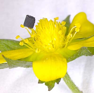
3D-printed graphene octet truss aerogel on strawberry blossom
3D-printed graphene octet truss aerogel on strawberry blossom. (Image: Virginia Tech)
Because of its strength – graphene is one of the strongest materials ever tested on Earth – and its high thermal and electricity conductivity, 3D printed graphene objects would be highly coveted in certain industries, including batteries, aerospace, separation, heat management, sensors, and catalysis.
Graphene is a single layer of carbon atoms organized in a hexagonal lattice. When graphene sheets are neatly stacked on top of each other and formed into a three-dimensional shape, it becomes graphite, commonly known as the “lead” in pencils.
Because graphite is simply packed-together graphene, it has fairly poor mechanical properties. But if the graphene sheets are separated with air-filled pores, the three-dimensional structure can maintain its properties. This porous graphene structure is called a graphene aerogel.
“Now a designer can design three-dimensional topology comprised of interconnected graphene sheets,” said Xiaoyu “Rayne” Zheng, assistant professor with the Department of Mechanical Engineering in the College of Engineering and director of the Advanced Manufacturing and Metamaterials Lab. “This new design and manufacturing freedom will lead to optimization of strength, conductivity, mass transport, strength, and weight density that are not achievable in graphene aerogels.”
Zheng, also an affiliated faculty member of the Macromolecules Innovation Institute, has received grants to study nanoscale materials and scale them up to lightweight and functional materials for applications in aerospace, automobiles, and batteries.
Previously, researchers could print graphene using an extrusion process, sort of like squeezing toothpaste, but that technique could only create simple objects that stacked on top of itself.
“With that technique, there’s very limited structures you can create because there’s no support and the resolution is quite limited, so you can’t get freeform factors,” Zheng said. “What we did was to get these graphene layers to be architected into any shape that you want with high resolution.”
This project began three years ago when Ryan Hensleigh, lead author of the article and now a third-year Macromolecular Science and Engineering Ph.D. student, began an internship at the Lawrence Livermore National Laboratory in Livermore, California. Hensleigh started working with Zheng, who was then a member of the technical staff at Lawrence Livermore National Laboratory. When Zheng joined the faculty at Virginia Tech in 2016, Hensleigh followed as a student and continued working on this project.
scanning electron microscope picture of a graphene octet-truss
Left: Zoomed-in scanning electron microscope picture of a graphene octet-truss at a resolution of 1 micrometer. Right: Zoomed-in scanning electron microscope picture of a graphene octet-truss at a resolution of 10 micrometers. (Image: Virginia Tech)
To create these complex structures, Hensleigh started with graphene oxide, a precursor to graphene, crosslinking the sheets to form a porous hydrogel. Breaking the graphene oxide hydrogel with ultrasound and adding light-sensitive acrylate polymers, Hensleigh could use projection micro-stereolithography to create the desired solid 3D structure with the graphene oxide trapped in the long, rigid chains of acrylate polymer. Finally, Hensleigh would place the 3D structure in a furnace to burn off the polymers and fuse the object together, leaving behind a pure and lightweight graphene aerogel.
“It’s a significant breakthrough compared to what’s been done,” Hensleigh said. “We can access pretty much any desired structure you want.”
The key finding of this work, which was recently published with collaborators at Lawrence Livermore National Laboratory in the journal Materials Horizons („Additive manufacturing of complex micro-architected graphene aerogels”), is that the researchers created graphene structures with a resolution an order of magnitude finer than ever printed. Hensleigh said other processes could print down to 100 microns, but the new technique allows him to print down to 10 microns in resolution, which approaches the size of actual graphene sheets.
“We’ve been able to show you can make a complex, three-dimensional architecture of graphene while still preserving some of its intrinsic prime properties,” Zheng said. “Usually when you try to 3D print graphene or scale up, you lose most of their lucrative mechanical properties found in its single sheet form.”
Source: Virginia Tech
Subscribe to a free copy of one of our daily
Nanowerk Newsletter Email Digests
with a compilation of all of the day’s news.
These articles might interest you as well:
Tranziția de transmisie a tulburărilor aduse se transformă în izolator fotonic topologic(Added disorder drives transition to photonic topological insulator)

Folosind valuri de lumină, cercetătorii au arătat că un sistem non-topologic devine topologic atunci când se adaugă o tulburare aleatorie: nici o lumină nu este transmisă prin interiorul structurii, dar lumina curge peste suprafață într-o manieră unidirecțională.
Sistemul topologic fotonic a fost fabricat prin utilizarea impulsurilor laser concentrate cu densități enorme de energie în gama gigawatt, gravarea ghidurilor de undă într-un mediu de sticlă cu silice de înaltă puritate. Ghidurile de undă au fost aranjate într-o structură de tip grafenie în fagure de miere.
Aceste ghiduri de undă paralele, care ghidează lumina ca fibrele de sticlă, sunt în acest caz proiectate nu ca niște linii drepte ci ca linii elicoidale, astfel încât propagarea luminii în direcția înainte corespunde cu un șurub în sensul acelor de ceasornic și în direcția inversă un șurub invers acelor de ceasornic

Posted: Aug 23, 2018

Added disorder drives transition to photonic topological insulator

(Nanowerk News) Research on insulators with topologically protected surface conductivity – in short: topological insulators – is currently in vogue. Topological materials may be able to replace semiconductor technology in the future.

Topological insulators are characterized by remarkable electrical properties. While these structures have insulating properties in their interior, their conductivity on the surface is extremely robust – to such a degree that in principle an electron current, once introduced, would never cease to flow: one speaks of a „topologically” protected current. Analogous to a stream of electrons, which are half- integer spin particles, so-called fermions, the principle of the topological insulator also works with light particles, so-called bosons, having integer spin.
The properties of a topological insulator are generally stable and persist even when disorder is added. Only a very large disorder in the regular structure can cause the conductive properties on the surface to vanish, resulting in a normal insulator. For photonic topological insulators, this regime of very large disorder means that no light at all can pass through the interior of such a structure, nor can it be transmitted on the surface.
In 2009, Chu, Jain, and Shen theoretically investigated electronic topological insulators with quite extraordinary properties. The starting point of their considerations was a normal insulator, which does not conduct electricity. In their numerical simulation, they showed that the characteristic properties of topological insulators – interior insulation and perfect conductance along the surface (edge) – can be generated by introducing random disorder of the structure. This hypothesis has thus far never been proven in an experiment.
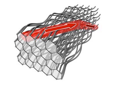
A honeycomb waveguide structure with helical waveguides acts as a photonic topological insulator so that light is guided along the surface
Fig. 1: A honeycomb waveguide structure with helical waveguides acts as a photonic topological insulator so that light is guided along the surface.
In a paper in Nature („Photonic Topological Anderson Insulators”), this hypothesis for electrons in solids was experimentally demonstrated for light waves by an international team of scientists based at the University of Rostock (Germany), the Technion (Israel), as well as Penn State University and the University of Maryland (U.S.). After extensive theoretical considerations and numerically complex simulations, an experimental design was implemented.
Using light waves, the researchers showed that a non-topological system becomes topological when random disorder is added: no light is transmitted through the interior of the structure, but light flows over the surface in a unidirectional fashion.
The photonic topological system was fabricated by using focused laser pulses with enormous energy densities in the gigawatt range, engraving waveguides into a high-purity fused-silica glass medium. The waveguides were arranged in a honeycomb graphene structure.
These parallel waveguides, which guide the light like glass fibers, are in this case designed not as straight lines but as helical lines, so that the propagation of the light in the forward direction corresponds to a clockwise screw and in the reverse direction a counterclockwise screw. This creates the diffraction properties of a topological insulator, where light circulates around the circumference of the helical array of waveguides in a single direction, and in a way that is immune to disorder such as a missing waveguide (Fig. 1).
However, when the helical honeycomb lattice is systematically modified so that the refractive index of adjacent waveguides is slightly different, the topological properties are destroyed: the light no longer flows on the surface in a unidirectional manner (Fig. 2). When a random disorder is added on top of this modified structure, the topological properties are fully recovered.
Adding further disorders to the refractive indices of the waveguides restores the topological properties so that light flows again along the surface of the structure
Fig. 2: Adding further disorders to the refractive indices of the waveguides restores the topological properties so that light flows again along the surface of the structure.
In the experimental setup, light from a red Helium Neon laser is coupled into the waveguide structure. At the other end of the waveguide structure, a camera detects whether light is transmitted through the structure or is transmitted on the surface. In a first experiment, the refractive indices of every adjacent waveguides were made to differ by two ten thousandths. Thus the conductive properties of the topological structure were completely destroyed: no light could be detected behind the structure. But what happens if further disorders are added to the existing disorder?
In a second experiment, the waveguides were prepared in such a way that irregularly distributed differences in the refractive indices of all waveguides were added to the existing regular disorder of adjacent waveguides. Contrary to the expectation that in the event of further disorder in the topological structure the purely insulating properties would be retained and it would remain dark in the sample, the second experiment showed light conduction across the surface. Light could indeed be detected at the edge.
Thus, in the case of light, the experimental proof of the hypothesis of Chu et al., which had originally been expressed only for electrons, has succeeded: by adding disorder, topological insulators can be generated from normal insulators, a highly counterintuitive result. The properties of topological materials as such are quite remarkable; however the dependence of their properties on disorder in the structure is even more extraordinary.
The novel findings of the international research group may contribute to further elucidating the bizarre properties of topological insulators.
“These findings shed new light onto the peculiar properties of topological insulators,” said Professor Alexander Szameit, principal investigator of the Rostock group and lead author of the publication. “This shows that using photonics, we have opened the door to understanding disordered topological insulators in a completely new way. Photonic topological systems could potentially be a route to overcoming parasitic disorder in both fundamental science and real-world applications.”
Professor Mordechai Segev of the Technion added: “The first photonic topological insulator for light was realized in 2013 through collaboration between my group, where the research was led by Mikael Rechtsman and Yonatan Plotnik, and the group of Alex Szameit (at that time in Jena, Germany). Two years later, Mikael Rechtsman and my young colleague Netanel Lindner wrote a theory paper that envisioned the current experiment. And now the experiment has become a reality through the efforts of Alex’s students in a beautiful paper which we all collaborated on. It is fascinating to see how this new field is being led by a group of young, very talented people like Mik, Netanel, Alex and their students, in three different countries.”
Source: Universität Rostock

Conductele laminate de la Graphene ar putea reduce coroziunea în industria de petrol și gaze(Graphene laminated pipes could reduce corrosion in the oil and gas industry)

Grafenul este primul material bidimensional din lume, flexibil, transparent, mai conductiv decât cuprul și este cunoscut că blochează trecerea heliului, cel mai greu gaz de blocat.Cercetătorii au descoperit că dacă grafenul a fost amestecat mecanic cu materialul plastic sau dacă s-a aplicat un singur strat de grafen, gazele ar fi putut să treacă.
Cu toate acestea, prin laminarea unui strat subțire de nanoplateste de grafen la poliamida 11 (PA11) – un material plastic folosit adesea în aceste căptușeli – echipa a reușit să producă structuri care se comportă ca niște bariere excepțional de bune.

Posted: Aug 22, 2018

Graphene laminated pipes could reduce corrosion in the oil and gas industry

(Nanowerk News) Researchers at The University of Manchester and TWI have discovered ways of using graphene to prolong the lifetime of pipes used in the oil and gas industry.

Published in Advanced Materials Interfaces („Graphene/Polyamide Laminates for Supercritical CO2 and H2S Barrier Applications: An Approach toward Permeation Shutdown „), the team have found a way of incorporating graphene into a polymer liner used in pipes that transport crude oil and gas from the sea floor.
The pipes are generally made of internal layers of polymer or composite and external strengthening steel. Within these pipes, fluids may be at very high pressure and elevated temperature.
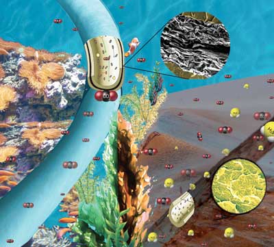
using graphene to prolong the lifetime of pipes used in the oil and gas industry
Using graphene to prolong the lifetime of pipes used in the oil and gas industry. (Image: University of Manchester)
In situations where carbon dioxide (CO2), hydrogen sulfide (H2S) and water permeate through the protective barrier layer of the pipe, the steel may corrode causing the pipe to lose strength over time, leading to a risk of catastrophic failure.
The researchers found that if the graphene was mechanically mixed with the plastic, or if a single layer of graphene were applied, gases were still able to pass through.
However, by laminating a thin layer of graphene nanoplatelets to polyamide 11 (PA11) – a plastic often used in these liners – the team were able to produce structures that behave as exceptionally good barriers.
The multi-layered laminate structures were tested at 60°C and at pressures up to 400 times atmospheric pressure, and were shown to reduce CO2 permeation by over 90% compared to PA11 alone, while permeation of H2S can be reduced to undetectable levels.
Graphene is the world’s first two-dimensional material, flexible, transparent, more conductive than copper, and is known to block the passage of helium, the hardest gas to block.
Corrosion costs the oil and gas industry in the US alone $1.4 billion. This technology has the potential to extend the life of the underwater pipework and therefore reduce the time between repairs.
Professor Peter Budd, who led the Manchester team, said: “Graphene has many amazing properties, but it is not always easy to realise them on a large scale. Our work represents an important step in taking graphene out of the laboratory and into the real world.”
Dr Paul Woollin, Director of Research, TWI, said: “This research is an example of how TWI can work effectively with world leading universities through its Innovation Network, and draw on our cutting edge testing capability and in house experts, to identify unique and novel solutions to industry’s most challenging problems.
Graphene membranes such as these have the potential to open up vast new markets and revolutionise countless industrial processes, such as food packaging, water filtration and gas separation.
Source: University of Manchester

Insulatorul topologic nou ar putea îmbunătăți eficiența procesării și memoriei computerului(New topological insulator could improve efficiency of computer processing and memory)

O echipă de cercetători condusă de Universitatea din Minnesota a dezvoltat un nou material care ar putea îmbunătăți eficiența procesării și memoriei computerului. Cercetatorii au depus un brevet asupra materialului cu sprijinul companiei de cercetare Semiconductor Corporation, iar oamenii din industria semiconductorilor au cerut deja mostre din material.Noul material se află într-o clasă de materiale numite „izolatoare topologice”, care au fost studiate recent de comunitățile de cercetare fizică și materiale și de industria semiconductorilor datorită transportului unic spin-electronic și proprietăților magnetice.

Posted: Aug 22, 2018

New topological insulator could improve efficiency of computer processing and memory

(Nanowerk News) A team of researchers led by the University of Minnesota has developed a new material that could potentially improve the efficiency of computer processing and memory. The researchers have filed a patent on the material with support from the Semiconductor Research Corporation, and people in the semiconductor industry have already requested samples of the material.

The findings are published in Nature Materials („Room-temperature high spin–orbit torque due to quantum confinement in sputtered BixSe(1–x) films”), a peer-reviewed scientific journal published by Nature Publishing Group.
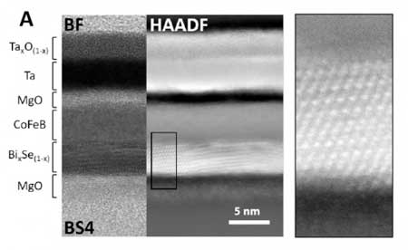
cross-sectional transmission electron microscope image shows a sample used for the charge-to-spin conversion experiment
This cross-sectional transmission electron microscope image shows a sample used for the charge-to-spin conversion experiment. The nano-sized grains of less than 6 nanometers in the sputtered topological insulator layer created new physical properties for the material that changed the behavior of the electrons in the material. (Image: Wang Group, University of Minnesota)
“We used a quantum material that has attracted a lot of attention by the semiconductor industry in the past few years, but created it in unique way that resulted in a material with new physical and spin-electronic properties that could greatly improve computing and memory efficiency,” said lead researcher Jian-Ping Wang, a University of Minnesota Distinguished McKnight Professor and Robert F. Hartmann Chair in electrical engineering.
The new material is in a class of materials called “topological insulators,” which have been studied recently by physics and materials research communities and the semiconductor industry because of their unique spin-electronic transport and magnetic properties. Topological insulators are usually created using a single crystal growth process. Another common fabrication technique uses a process called Molecular Beam Epitaxy in which crystals are grown in a thin film. Both of these techniques cannot be easily scaled up for use in the semiconductor industry.
In this study, researchers started with bismuth selenide (Bi2Se3), a compound of bismuth and selenium. They then used a thin film deposition technique called “sputtering,” which is driven by the momentum exchange between the ions and atoms in the target materials due to collisions. While the sputtering technique is common in the semiconductor industry, this is the first time it has been used to create a topological insulator material that could be scaled up for semiconductor and magnetic industry applications.
However, the fact that the sputtering technique worked was not the most surprising part of the experiment. The nano-sized grains of less than 6 nanometers in the sputtered topological insulator layer created new physical properties for the material that changed the behavior of the electrons in the material. After testing the new material, the researchers found it to be 18 times more efficient in computing processing and memory compared to current materials.
“As the size of the grains decreased, we experienced what we call ‘quantum confinement’ in which the electrons in the material act differently giving us more control over the electron behavior,” said study co-author Tony Low, a University of Minnesota assistant professor of electrical and computer engineering.
Researchers studied the material using the University of Minnesota’s unique high-resolution transmission electron microscopy (TEM), a microscopy technique in which a beam of electrons is transmitted through a specimen to form an image.
“Using our advanced aberration-corrected scanning TEM we managed to identify those nano-sized grains and their interfaces in the film,” said Andre Mkhoyan, a University of Minnesota associate professor of chemical engineering and materials science and electron microscopy expert.
Researchers say this is only the beginning and that this discovery could open the door to more advances in the semiconductor industry as well as related industries, such as magnetic random access memory (MRAM) technology.
“With the new physics of these materials could come many new applications,” said Mahendra DC (Dangi Chhetri), first author of the paper and a physics Ph.D. student in Professor Wang’s lab.
Wang agrees that this cutting-edge research could make a big impact.
“Using the sputtering process to fabricate a quantum material like a bismuth-selenide-based topological insulator is against the intuitive instincts of all researchers in the field and actually is not supported by any existing theory,” Wang said. “Four years ago, with a strong support from Semiconductor Research Corporation and the Defense Advanced Research Projects Agency, we started with a big idea to search for a practical pathway to grow and apply the topological insulator material for future computing and memory devices. Our surprising experimental discovery led to a new theory for topological insulator materials.
“Research is all about being patient and collaborating with team members. This time there was a big pay off,” Wang said.
Source: University of Minnesota College of Science and Engineering

O singura data , o barieră de performanță, un aspect material ar putea îmbunătăți telecomunicațiile(Once a performance barrier, material quirk could improve telecommunications)

au arătat cum poate fi proiectat un material feroelectric în așa fel încât pereții domeniului pot fi utilizați pentru a transmite microunde cu un grad mai mare de control al frecvenței decât dispozitivele mobile pe care le folosim în prezent;au simulat comportamentul dinamic la scară atomică a materialului special de film la diferite valori ale temperaturii, tensiunii și câmpului electric, comparându-l cu cel pentru o „perfect” cristal feroelectric fără pereți de domenii – ceea ce a evidențiat comportamentul excepțional al materialului.

Posted: Aug 21, 2018

Once a performance barrier, material quirk could improve telecommunications

(Nanowerk News) Researchers who study and manipulate the behavior of materials at the atomic level have discovered a way to make a thin material that enhances the flow of microwave energy. The advance, which could improve telecommunications, sheds new light on structural traits, generally viewed as static and a hindrance, that, when made to be dynamic, are actually key to the material’s special ability.

The discovery, reported in the journal Nature („Resonant domain-wall-enhanced tunable microwave ferroelectrics”), shows how domain walls – the naturally occurring boundaries, separating atoms with different directions of relative displacement, that create dipoles within a material – could actually be an entryway for accessing a much wider range of electromagnetic frequencies. And this access could one day expand the range of frequencies used as communications channels.
Domain-Wall Variant Ferroelectric Material
Artist’s top-view rendering of a domain wall-variant material featuring a diffuse boundary separating aligned-dipole regions in a ferroelectric crystal film. Tunable, resonant fluctuations of these two-dimensional defects enable reduction of microwave radio frequency dielectric losses to beyond the crystal’s intrinsic limit. (Image: Drexel University)
In the paper, researchers from Drexel University, Bar-Ilan University in Israel, the University of California at Berkeley, the University of California at Santa Barbara, the Carnegie Institution for Science, and the University of Pennsylvania showed how a ferroelectric material can be designed in such a way that domain walls can be used to transmit microwaves with a higher degree of frequency control than the mobile devices we currently use.
„As consumer demand for mobile communications increases the available wireless spectrum is increasingly congested and new technologies are needed to create adaptive, frequency-agile antennas,” said Robert York, a professor at UC Santa Barbara and a co-author of the paper. „Tunable dielectric materials could be a potential solution.”
Using the domain walls within a material to enhance its transmission quality is a particularly unexpected approach because the presence of these boundaries tends to strongly diminish a material’s ability to pass a microwave electromagnetic field. Until now, the best film materials for transmitting electromagnetic fields in radio-frequency devices were generally considered to be single-crystal materials that do not have any permanent dipole moments – let alone domain walls.
But the research team turned this perception of domain walls on its head by creating a ferroelectric material with a high density of domain walls, that can outperform single crystals when it comes to tunability and transmission quality.
The group found that the domain walls of a thin film of barium strontium titanate, a frequently studied ferroelectric material, function like vibrating guitar strings that resonate together. Rather than absorbing or scattering microwaves, the presence of a dense, but ordered, thicket of oscillating domain walls actually improves the quality of the transmission.
„Even the best-quality bulk single crystals, without permanent, re-orientable dipoles, have higher losses at higher frequencies, due to interference caused by the vibrations of atoms in the lattice,” said Jonathan Spanier, a materials science professor at Drexel who led the research. „Film materials with permanent dipoles form domain walls, and the loss is much worse. But films that support reversible domain wall motion and their oscillating behavior surprisingly break that trend and resonate over a wide range of frequencies.”
According to the researchers, „the proximity of and accessibility among thermodynamically predicted strain-induced, ferroelectric domain wall variants to achieve gigahertz microwave tunability and dielectric loss that surpass those for the current best film devices by 1-2 orders of magnitude, attaining values comparable to bulk single crystals, but in an intrinsically tunable material,” they write in the paper.
The key to this exceptional tunability, according to co-author Zongquan Gu, a postdoctoral scientist in Spanier’s research group, is the abundance of different phases, „the ferroelectric phase transition temperature marks the onset of the permanent dipolar ordering. A peak in the dielectric susceptibility, a thermodynamic property related to the magnitude of capacitance, is a hallmark of the transition,” Gu said. „Engineering a film material to have many, more easily available ‘phases’ near the transition allows the material to attain much higher capacitance tuning with the same voltage.”
Along with Spanier, Gu, and Geoffrey Xiao, an undergraduate student at Drexel, launched theory and simulation efforts for the prediction of domain wall-rich energy landscapes to direct the production of the domain wall-rich barium strontium titanate film. With Spanier’s colleagues at Berkeley, led by Lane Martin, professor in materials science, a leader in ferroelectric domain walls film science, Gu also made and characterized the first samples of the material, using a process called strain engineering to create a dense concentration of domain walls.
From there, collaborators from Bar-Ilan University in Israel led by Ilya Grinberg, a professor of chemistry, simulated the atomic-scale dynamic behavior of the special film material at different values of temperature, strain and electric field, comparing it with that for a „perfect” ferroelectric crystal without any domain walls – which revealed the material’s exceptional behavior.
This intrinsic tunability, meaning the material’s excellent transmission abilities do not require any external, electromechanical enhancement, make it promising for use in communication devices – where efficient access to spectrum is essential.
At UC Santa Barbara, York, a professor of electrical and computer engineering, and his doctoral student Cedric Meyers, fabricated electrode test structures that enabled the measurement and analysis of material’s resonant microwave response, including its tunability.
„Tunable dielectric materials have been a focus of investigation in my group at UCSB since the late 1990s,” York said. „But despite some progress early on, we consistently ran up against limitations of the materials that were poorly understood. This work helps to better understand these limitations and to identify potential solutions.”
Source: Drexel University

O nouă generație de retine artificiale bazată pe materiale 2D(A new generation of artificial retinas based on 2D materials)

Oamenii de stiinta sustin ca au dezvoltat si testat cu succes prima retina artificiala ultrathina din lume, care ar putea imbunatatii considerabil tehnologia vizuala implantabila existenta pentru orb. Dispozitivul flexibil, bazat pe materiale foarte subțiri 2D, ar putea reveni într-o zi la milioane de oameni cu boli retiniene. Și cu câteva modificări, dispozitivul ar putea fi folosit pentru a urmări activitatea inimii și a creierului.
Cercetatorii isi prezinta lucrarile astazi la cea de-a 256-a reuniune nationala si expozitie a Societatii Americane de Chimie (ACS).
Aceasta este prima demonstratie pe care o puteti folosi grafenul cu cateva straturi si disulfura de molibden pentru fabricarea cu succes a unei retini artificiale „, spune Nanshu Lu, Ph.D. Desi aceasta cercetare este inca in faza incipienta, este un punct de plecare foarte interesant pentru utilizarea acestor materiale pentru a restabili viziunea, spune ea, adaugand ca acest dispozitiv ar putea fi, de asemenea, implantat in alta parte a corpului pentru a monitoriza activitatile inimii si creierului.

Posted: Aug 20, 2018

A new generation of artificial retinas based on 2D materials

(Nanowerk News) Scientists report they have successfully developed and tested the world’s first ultrathin artificial retina that could vastly improve on existing implantable visualization technology for the blind. The flexible device, based on very thin 2D materials, could someday restore sight to the millions of people with retinal diseases. And with a few modifications, the device could be used to track heart and brain activity.

The researchers are presenting their work today at the 256th National Meeting & Exposition of the American Chemical Society (ACS).
“This is the first demonstration that you can use few-layer graphene and molybdenum disulfide to successfully fabricate an artificial retina,” Nanshu Lu, Ph.D., says. “Although this research is still in its infancy, it is a very exciting starting point for the use of these materials to restore vision,” she says, adding that this device could also be implanted elsewhere in the body to monitor heart and brain activities.
The retina, located at the back of the eye, contains specialized photoreceptor cells called rods and cones that convert incoming light into nerve signals. These impulses travel into the brain via the optic nerve where they are decoded into visual images.
Diseases such as macular degeneration, diabetic retinopathy and retinitis pigmentosa can damage or destroy retinal tissue, leading to vision loss or complete blindness. There is no cure for many of these diseases, but silicon-based retinal implants have restored a modicum of vision to some individuals.
However, Lu says these devices are rigid, flat and fragile, making it hard for them to replicate the natural curvature of the retina. As a result, silicon-based retinal implants often produce blurry or distorted images and can cause long-term strain or damage to surrounding eye tissue, including the optic nerve.
Lu, who is at the University of Texas at Austin, and her collaborator Dae-Hyeong Kim, Ph.D., who is at Seoul National University, sought to develop a thinner, more flexible alternative that would better mimic the shape and function of a natural retina.
The researchers used 2D materials, including graphene and molybdenum disulfide, as well as thin layers of gold, alumina and silicon nitrate to create a flexible, high-density and curved sensor array. The device, which resembles the surface of a flattened soccer ball or icosahedron, conforms to the size and shape of a natural retina without mechanically disturbing it.
In laboratory and animal studies, photodetectors on the device readily absorbed light and passed it through a soft external circuit board. The circuit board housed all of the electronics needed to digitally process light, stimulate the retina and acquire signals from the visual cortex.
Based on these studies, the researchers determined that this prototype artificial retina is biocompatible and successfully mimics the structural features of the human eye. They say it could be an important step in the quest to develop the next generation of soft bio-electronic retinal prostheses.
Moving ahead, Lu is exploring ways to integrate this technology into mechanically and optically imperceptible electronic tattoos that are laminated on the skin surface to gather real-time health information. Lu says that the team plans to add transistors to these transparent e-tattoos to help amplify signals from the brain or the heart so they can be more easily monitored and treated.
These ultrathin sensors and electrodes can also be implanted on the surface of the heart to detect arrhythmias. Lu says doctors could potentially program them to act like tiny pacemakers, sending electrical impulses through the heart to correct the problem.

Title: 2D Materials based on Epidermal and Implantable Conformal Electronics

Abstract :Bio-tissues are soft, curvilinear and dynamic whereas wafer-based electronics are hard, planar, and fragile. Such mismatch fundamentally impedes their integration with each other. As atomically thin, optically transparent, mechanically robust, and highly functional electronic materials, 2D materials are ideal for conformable bioelectronics. We have invented a cost- and time-effective “wet transfer, dry patterning” process for the freeform manufacture of graphene e-tattoos (GETs). Our GET has a total thickness of less than 500 nm, an optical transparency of ~85%, and a stretchability of more than 40%. Tensile fracture of PMMA-supported graphene has been experimentally investigated and different stages of fracture have been identified. GET can be directly laminated on human skin exactly like a temporary transfer tattoo and can fully conform to the microscopic morphology of the skin surface via just van der Waals forces. Analytical models are developed to guide the GET design for full skin conformability even under skin deformation [4]. As a dry electrode, GET-skin interface impedance is found to be as low as medically used Ag/AgCl gel electrodes. GET has been successfully applied to measure electrocardiogram (ECG), electromyogram (EMG), electroencephalogram (EEG), skin temperature, and skin hydration. When applied around human eyes, imperceptible GET electrooculogram (EOG) sensors can capture eye movement with an angular resolution of 4 degrees, which can be used to wirelessly control a quadcopter in real-time. In addition to noninvasive e-tattoos, we have engineered human eye-inspired soft implantable optoelectronic device using atomically thin MoS2-graphene heterostructure and strain-releasing, retina conformable designs. The hemispherically curved image sensor array exhibits infrared blindness and successfully acquires pixelated optical signals. We propose the ultrathin hemispherically curved image sensor array as a promising imaging element in the soft retinal implant with minimum mechanical loading to the retina. Optical signals obtained by this curved image array can be converted to electrical stimulations applied to optic nerves to restore visualization.
Source: American Chemical Society

Bateriile sunt pregătite pentru revoluția organică(Batteries poised for organic revolution)

Crucial, noul material este, de asemenea, robust, rămânând stabil peste mii de cicluri de încărcare / descărcare a bateriei.
Catodul, electrodul pozitiv în bateriile Li-ion, este o componentă critică. O moleculă organică cu deficit de electroni, numită hexazatrin-naftalină (HATN), a fost investigată anterior ca material catodic organic pentru bateriile cu litiu-ion. Cu toate acestea, performanța sa promițătoare inițială a scăzut rapid în timpul utilizării, deoarece molecula a început să se dizolve în electrolitul lichid al bateriei.

Posted: Aug 16, 2018

Batteries poised for organic revolution

(Nanowerk News) Incorporating organic materials into lithium ion batteries could lower their cost and make them more environmentally friendly, A*STAR researchers have found (Journal of Materials Chemistry A, „Hexaazatriphenylene derivatives/GO composites as organic cathodes for lithium ion batteries”).

The team has developed an organic-based battery cathode that has significantly improved electrochemical performance compared to previous organic cathode materials. Crucially, the new material is also robust, remaining stable over thousands of battery charge/discharge cycles.
The cathode, the positive electrode in Li-ion batteries, is a critical component. An electron-deficient, rigid organic molecule called hexaazatrinaphthalene (HATN) was previously investigated as an organic cathode material for lithium ion batteries. However, its promising initial performance declined rapidly during use, because the molecule began to dissolve into the battery’s liquid electrolyte.
A new cathode material, in which HATN was combined with graphene oxide in a bid to prevent the organic material from dissolving, has now been developed by Yugen Zhang and his colleagues from the A*STAR Institute of Bioengineering and Nanotechnology.
Hydrogen bonds (blue) strongly attach the redox active organic molecule HATNTA (red) to a graphene oxide support (grey)
Hydrogen bonds (blue) strongly attach the redox active organic molecule HATNTA (red) to a graphene oxide support (grey). (© The Royal Society of Chemistry)
In graphene oxide, a single-atom thick sheet of carbon atoms is partly covered by a layer of oxygen atoms. “Graphene oxide has excellent electronic conductivity, and surface oxygen functionality that may form hydrogen-bonding interactions with HATN,” Zhang says. He explains that this made graphene oxide a promising candidate for forming a HATN-graphene oxide nanocomposite.
The nanocomposite’s performance exceeded expectations. The materials combined to form core-shell nanorods in which the HATN was coated with graphene oxide. “Graphene oxide and HATN formed a very nice composite structure, which solved the dissolution issue of HATN in electrolyte and gave the cathode very good cycling stability,” Zhang says. A lithium ion battery using this material as its cathode retained 80 per cent of its capacity after 2000 charge/discharge cycles.
The team saw even better performance when they combined graphene oxide with a HATN derivate called hexaazatrinaphthalene tricarboxylic acid (HATNTA). A battery made from this material retained 86 per cent of its capacity after 2,000 charge/discharge cycles. The improved performance is probably due to the polar carboxylic acid groups on the HATNTA molecule, which attached the molecule even more strongly to the graphene oxide.
The team is continuing to develop new materials to improve the performance of organic cathodes, Zhang says. Aside from investigating alternatives to graphene oxide, the team also is working on HATN-based porous polymers for use as organic cathode materials, which should enhance the flow of ions during battery charge and discharge.
Source: A*STAR