Oamenii pot simți diferențele moleculare între suprafețe aproape identice(Humans can feel molecular differences between nearly identical surfaces)

De asemenea, este interesant faptul că dispozitivul cu degetul fals, care nu are nimic asemănător cu sutele de nervi din pielea noastră, are doar un senzor de forță și este în continuare capabil să obțină informațiile necesare pentru a simți diferența în aceste suprafețe. nu doar mecanoreceptorii din piele, ci și receptorii din ligamente, articulații, încheieturi, cot și umăr care ar putea permite oamenilor să perceapă diferențele minime prin atingere

Posted: Dec 13, 2017

Humans can feel molecular differences between nearly identical surfaces

(Nanowerk News) How sensitive is the human sense of touch? Sensitive enough to feel the difference between surfaces that differ by just a single layer of molecules, a team of researchers at the University of California San Diego has shown.

„This is the greatest tactile sensitivity that has ever been shown in humans,” said Darren Lipomi, a professor of nanoengineering and member of the Center for Wearable Sensors at the UC San Diego Jacobs School of Engineering, who led the interdisciplinary project with V. S. Ramachandran, director of the Center for Brain and Cognition and distinguished professor in the Department of Psychology at UC San Diego.
Humans can easily feel the difference between many everyday surfaces such as glass, metal, wood and plastic. That’s because these surfaces have different textures or draw heat away from the finger at different rates. But UC San Diego researchers wondered, if they kept all these large-scale effects equal and changed only the topmost layer of molecules, could humans still detect the difference using their sense of touch? And if so, how?
Researchers say this fundamental knowledge will be useful for developing electronic skin, prosthetics that can feel, advanced haptic technology for virtual and augmented reality and more.
Unsophisticated haptic technologies exist in the form of rumble packs in video game controllers or smartphones that shake, Lipomi added. „But reproducing realistic tactile sensations is difficult because we don’t yet fully understand the basic ways in which materials interact with the sense of touch.”
„Today’s technologies allow us to see and hear what’s happening, but we can’t feel it,” said Cody Carpenter, a nanoengineering Ph.D. student at UC San Diego and co-first author of the study. „We have state-of-the-art speakers, phones and high-resolution screens that are visually and aurally engaging, but what’s missing is the sense of touch. Adding that ingredient is a driving force behind this work.”
This study is the first to combine materials science and psychophysics to understand how humans perceive touch. „Receptors processing sensations from our skin are phylogenetically the most ancient, but far from being primitive they have had time to evolve extraordinarily subtle strategies for discerning surfaces–whether a lover’s caress or a tickle or the raw tactile feel of metal, wood, paper, etc. This study is one of the first to demonstrate the range of sophistication and exquisite sensitivity of tactile sensations. It paves the way, perhaps, for a whole new approach to tactile psychophysics,” Ramachandran said.

Super-sensitive touch

In a paper published in Materials Horizons („Human ability to discriminate surface chemistry by touch”), UC San Diego researchers tested whether human subjects could distinguish–by dragging or tapping a finger across the surface–between smooth silicon wafers that differed only in their single topmost layer of molecules. One surface was a single oxidized layer made mostly of oxygen atoms. The other was a single Teflon-like layer made of fluorine and carbon atoms. Both surfaces looked identical and felt similar enough that some subjects could not differentiate between them at all.
According to the researchers, human subjects can feel these differences because of a phenomenon known as stick-slip friction, which is the jerking motion that occurs when two objects at rest start to slide against each other. This phenomenon is responsible for the musical notes played by running a wet finger along the rim of a wine glass, the sound of a squeaky door hinge or the noise of a stopping train. In this case, each surface has a different stick-slip frequency due to the identity of the molecules in the topmost layer.
In one test, 15 subjects were tasked with feeling three surfaces and identifying the one surface that differed from the other two. Subjects correctly identified the differences 71 percent of the time.
In another test, subjects were given three different strips of silicon wafer, each strip containing a different sequence of 8 patches of oxidized and Teflon-like surfaces. Each sequence represented an 8-digit string of 0s and 1s, which encoded for a particular letter in the ASCII alphabet. Subjects were asked to „read” these sequences by dragging a finger from one end of the strip to the other and noting which patches in the sequence were the oxidized surfaces and which were the Teflon-like surfaces. In this experiment, 10 out of 11 subjects decoded the bits needed to spell the word „Lab” (with the correct upper and lowercase letters) more than 50 percent of the time. Subjects spent an average of 4.5 minutes to decode each letter.
„A human may be slower than a nanobit per second in terms of reading digital information, but this experiment shows a potentially neat way to do chemical communications using our sense of touch instead of sight,” Lipomi said.

Basic model of touch

The researchers also found that these surfaces can be differentiated depending on how fast the finger drags and how much force it applies across the surface. The researchers modeled the touch experiments using a „mock finger,” a finger-like device made of an organic polymer that’s connected by a spring to a force sensor. The mock finger was dragged across the different surfaces using multiple combinations of force and swiping velocity. The researchers plotted the data and found that the surfaces could be distinguished given certain combinations of velocity and force. Meanwhile, other combinations made the surfaces indistinguishable from each other.
„Our results reveal a remarkable human ability to quickly home in on the right combinations of forces and swiping velocities required to feel the difference between these surfaces. They don’t need to reconstruct an entire matrix of data points one by one as we did in our experiments,” Lipomi said.
„It’s also interesting that the mock finger device, which doesn’t have anything resembling the hundreds of nerves in our skin, has just one force sensor and is still able to get the information needed to feel the difference in these surfaces. This tells us it’s not just the mechanoreceptors in the skin, but receptors in the ligaments, knuckles, wrist, elbow and shoulder that could be enabling humans to sense minute differences using touch,” he added.
Source: University of California – San Diego

Noua membrana ultra-subtire de diamant Este cel mai bun prieten al radiobiologului(New ultra-thin diamond membrane Is a radiobiologist’s best friend)

a dezvoltat o membrană ultra-subțire de diamant care poate măsura numărul de protoni într-o doză de radiație cu o precizie aproape perfectă. Detectorul se atașează la un microbeam cu particule încărcate și permite transmiterea radiației într-o zonă mai mică de 2 micrometri

Posted: Dec 13, 2017

New ultra-thin diamond membrane Is a radiobiologist’s best friend

(Nanowerk News) Depending on the dose and the target, radiation can cause incredible damage to healthy cells or it can be used to treat cancer and other diseases. To understand how cells respond to different doses of radiation, scientists need to direct precise amounts of energy to specific areas of the cell. Measuring dosage can be challenging, however, especially when working with low-energy protons.

A collaboration of researchers from the Université de Bordeaux, Centre National de la Recherche Scientifique and CEA-LIST has developed an ultra-thin diamond membrane that can measure the number of protons in a dose of radiation with almost perfect accuracy. The detector attaches to a charged-particle microbeam and enables the delivery of radiation to an area less than 2 micrometers wide. The study, published this week in Applied Physics Letters, („Cell micro-irradiation with MeV protons counted by an ultra-thin diamond membrane”), represents a valuable technological advance for radiation biology.
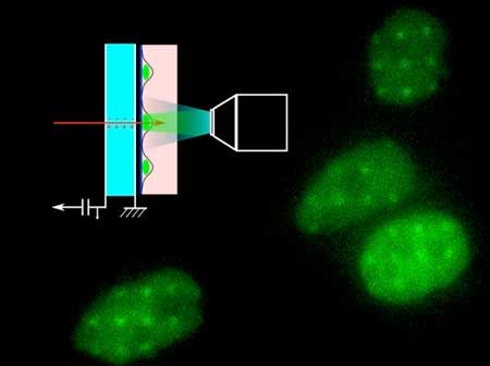
ultra-thin diamond membrane detects individual protons as they pass through
The ultra-thin diamond membrane detects individual protons as they pass through, allowing researchers to irradiate micron-sized areas on living cells for radiobiology experiments. (Image: Philippe Barberet)
Previous experiments had already established that diamond membranes can detect and quantify protons, but until the current study, no one had developed the technology for biological investigations.
“The device is completely compatible with living cells in their liquid environment,” said Philippe Barberet, a biophysicist at the Université de Bordeaux. “It will allow us to irradiate different kinds of cells and organisms using single protons, which is not so easy to do using low-energy accelerators.”
To test the effectiveness of the diamond membranes when irradiating live cells, the group used a cell line engineered to express a DNA repair protein called XRCC1, tagged with green fluorescent protein (GFP). When DNA damage occurs in these cells, the GFP lights up at the site of the repairs.
“XRCC1 is involved in DNA repair pathways and it’s one of the first proteins recruited,” said Barberet. “You irradiate and you immediately see an effect.” They delivered 100 protons spaced 5 micrometers apart to the cells. The resulting pattern of green irradiation spots confirmed that the beam inflicted damage in circles measuring less than 2 microns across.
The diamond membranes could become a valuable tool for increasing precision in radiation biology research. The researchers note, however, that their utility is limited to groups who have access to proton beams from particle accelerators.
Source: American Institute of Physics

Vehiculele ar putea obține „nervii” acel prejudiciu sens cu noi cercetări(Vehicles could get ‘nerves’ that sense damage with new research)

Elicopterele, rezervoarele și alte vehicule ar putea fi făcute într-o bună zi dintr-un „material inteligent” care să simtă daune, similar cu modul în care nervii spun organismului că a fost rănit, Ideea este că materialul sensibil din punct de vedere magnetic ar fi încorporat în materialul inteligent de pe întregul vehicul și va acționa ca un senzor care spune: „Avem daune aici”

Posted: Dec 13, 2017

Vehicles could get ‘nerves’ that sense damage with new research

(Nanowerk News) Helicopters, tanks and other vehicles could someday be made of „smart material” that senses damage, similar to how nerves tell the body it has been injured, with the help of new research based at Clemson University and funded by the U.S. Army Research Laboratory.

The idea is that magnetically sensitive material would be embedded within the smart material throughout the vehicle and act as a sensor that says, „Ouch! We have damage here,” said Oliver Myers, an associate professor of mechanical engineering.
Just as pain is relayed to the brain, the damage report would go to a computer and help determine whether a vehicle should keep going or return to the depot.
„In the field, we need that self-diagnostic capability,” Myers said. „Lieutenant Data in ‘Star Trek’ always says, ‘I’m performing to specified parameters.’ We want to make sure our platforms are performing to those specified parameters at a minimum.”
Myers is receiving $993,492 from the U.S. Army Research Laboratory to lead the project.
Oliver Myers (right) and mechanical engineering master's student Brandon Williams
Oliver Myers (right) and mechanical engineering master’s student Brandon Williams work with some of the smart material they are developing at Clemson University. (Image: Clemson University)
The research could help the Army save money on rotorcraft maintenance, said Asha Hall, the lead co-principal investigator and Prognostics and Diagnostics Acting Team Lead within the Mechanics Division of the Vehicle Technology Directorate at the U.S. Army Research Laboratory.
As a safety measure, the Army replaces some parts based on how long they have been in service, whether they appear damaged or not, she said. Embedded sensors could make it possible for parts to remain in service longer, based on their condition, Hall said.
„We’re trying to extend that maintenance-free operating period,” she said. „The big, big impact is to reduce sustainment costs for the Army.”
The research builds on the fast-growing field of composite materials, which are used in a variety of products from cars to airplanes. Composite materials often look and feel like plastic but are lighter and stronger than metals, including steel.
The team is sandwiching „magnetostrictive” material between multiple layers of composite materials, creating a laminate. The magnetostrictive material responds to a magnetic field or a change in stress, allowing it to act as the nerve that senses the damage.
„The composite laminate effectively becomes a smart structure,” Myers said.
The types of damage it could detect include impacts, cracking and unusual loading, he said.
Part of what makes the team’s approach unique is that the magnetostrictive material that senses the damage is embedded in the structure itself during the fabrication process, rather than attaching sensors after the structure is already built. Those external sensors often require additional equipment, Myers said.
The magnetostrictive material requires no power, is lightweight and operates in harsh environments, he said.
Richard Figliola, acting chair of the Department of Mechanical Engineering, said that Myers was well qualified to lead the research.
„Dr. Myers has deep experience in smart materials and smart structure mechanics of systems ranging from nano- to macro-scales sizes,” Figliola said. „He has written journal articles and attended conferences to develop relationships with his collaborators. The award is well deserved.”
Myers said the research was inspired by his master’s work in the Mechanical Engineering Department at the University of Maryland, Baltimore County, where he studied under the Meyerhoff Scholarship Program. That’s when he began playing with the idea of embedding materials in composite structures to see if damage could be detected.
At the time, he did it on a small scale.
Deployment to the field could be 10-20 years away, but Myers aims to move the research in that direction.
The central question Myers is asking is how the team can create a „robust sensing operation” using the embedded magnetostrictive material. Robust would mean it is observable, repeatable, measurable and sustainable, he said.
„We want this to not only be a benchtop experiment, but we want to be able to put it on larger structures and larger systems so that once we go from the benchtop coupon level we go to a full-size system and have it function as an NDE, or nondestructive evaluation, structural health-monitoring platform,” he said.
Anand Gramopadhye, dean of the College of Engineering, Computing and Applied Sciences, congratulated Myers on the award.
„His cutting-edge, innovative research could produce discoveries that have a significant impact on operational capabilities and technologies for the Army,” Gramopadhye said. „The amount of the award is a testament to his hard work, the creativity of his approach and his leadership in creating smart materials.”
Source: Clemson University

Drumul umed la baterii rapide și stabile(The wet road to fast and stable batteries)

a descoperit un material cu baterii anodice cu incarcare superficiala si operare stabila pe mai multe mii de cicluri.Echipa de cercetatori a urmarit modul in care compozitia si structura materialului s-au schimbat atunci cand au fost incalzite folosind diferite tehnici avansate de caracterizare, incluzand difractia de raze X furnizata de Advanced Photon Source, o Office DOE Office of Science Facility situat la Argonne. Atunci când analizează datele de caracterizare combinate, echipa a raportat că apa captată din materialul anodului a îmbunătățit performanța prin promovarea diversității structurale și formării nanostructurilor. Videoclipul de mai sus arată modificarea compoziției și a structurii, deoarece materialul de pornire este încălzit și apa este expulzată pentru a forma o nouă structură stratificată (LS), apoi o nanostructură hidratată dorită (HN), apoi dincolo de structura dorită, până la un nivel complet descompunerea nanostructurii (DN).

Posted: Dec 13, 2017

The wet road to fast and stable batteries

(Nanowerk News) An international team of scientists — including several researchers from the U.S. Department of Energy’s (DOE) Argonne National Laboratory — has discovered an anode battery material with superfast charging and stable operation over many thousands of cycles.

Over the last several decades, a multidisciplinary team of battery scientists at Argonne helped launch the modern energy storage race by conducting extensive research on a host of materials for lithium-ion batteries with applications in hybrid and all-electric vehicles, as well as stationary energy storage for buildings and the electric grid.
By heating the anode material to a much lower temperature, scientists could remove the water near the surface, but retain the water in the bulk of the material, which enhanced its characteristics
By heating the anode material to a much lower temperature (less than 260°C), scientists could remove the water near the surface, but retain the water in the bulk of the material, which enhanced its characteristics. (Image: Nature Communications and study authors)
One of Argonne’s latest contributions to innovative new materials for lithium-ion batteries is a water-bearing compound, “lithium titanate hydrate,” developed in collaboration with researchers from Tsinghua University in Beijing and the Massachusetts Institute of Technology. This material, discussed in a recent Nature Communications article („Lithium titanate hydrates with superfast and stable cycling in lithium ion batteries”), could replace the graphite anode commonly used in lithium-ion batteries.
As Jun Lu, Argonne battery scientist and co-author, explained, past research had identified lithium titanate as a promising anode material because of its potential for fast charging and long cycle life, as well as safer operation compared with graphite. In synthesizing this material, researchers used a water-based process that involved a final step of heating the anode material to very high temperature (above 500°C) to drive out the water completely. This step was needed because, during battery operation with this material, the water would react with the electrolyte and degrade performance.
Argonne Distinguished Fellow Khalil Amine, who also co-authored the study, noted that the heating to such a high temperature caused unwanted coarsening and clumping of the structure. The international team found that, by heating the anode material to a much lower temperature (less than 260°C), they could remove the water near the surface, but retain the water in the bulk of the material without coarsening and clumping of the structure. When the scientists tested the material in the laboratory, cycling stability improved and capacity degraded only slightly over 10,000 cycles. The material also charged very quickly — within less than two minutes — the team found. As noted by Jun Lu, “Most of the time, water is bad for non-aqueous lithium-ion batteries. But in this case, it can be downright good.”
The video shows the change in composition and structure as the starting material is heated and water is expelled to form a new layered structure (LS), then the desired hydrated nanostructure (HN), then beyond the desired structure all the way to a completely dehydrated nanostructure (DN).
The research team tracked how material composition and structure changed when heated by using various advanced characterization techniques, including x-ray diffraction provided by the Advanced Photon Source, a DOE Office of Science User Facility located at Argonne. When analyzing the combined characterization data, the team reported that the trapped water in the anode material improved performance by promoting structural diversity and forming nanostructures. The video above shows the change in composition and structure as the starting material is heated and water is expelled to form a new layered structure (LS), then the desired hydrated nanostructure (HN), then beyond the desired structure all the way to a completely dehydrated nanostructure (DN).
Looking to the future, Jun Lu observed that, because water is everywhere in nature and common in chemical synthesis, the fabrication approach reported in this research could open the door to discovery of other high-performance electrode materials.
Source: Argonne National Laboratory

Vehiculele ar putea deveni „nervi” , acel prejudiciu cu noi cercetari(Vehicles could get ‘nerves’ that sense damage with new research)

Ideea este că materialul sensibil din punct de vedere magnetic ar fi încorporat în materialul inteligent în întregul vehicul și va acționa ca un senzor;raportul privind daunele se va deplasa la un computer și va ajuta să se determine dacă un vehicul ar trebui să se răcească sau să se întoarcă la depozit

Vehicles

Oamenii de stiinta sugereaza nitrura de titan in loc de aur in optoelectronica(Scientists sug­gest ti­ta­ni­um nit­ri­de in­ste­ad of gold in op­to­e­lec­tro­nics)

Nitridatul de titan are proprietăți excelente anti-coroziune și stabilitate termică, este netoxic și sintetizat ușor și ieftin, iar acest lucru este extrem de important pentru aplicarea sa practică – spre deosebire de aurul și argintul obișnuit

Posted: Dec 12, 2017

Scientists sug­gest ti­ta­ni­um nit­ri­de in­ste­ad of gold in op­to­e­lec­tro­nics

(Nanowerk News) An international team of scientists from Russia, Sweden and the USA suggested replacing gold and silver, which are used in optoelectronic devices, with an inexpensive material of titanium nitride. The results of the study are published in the journal Applied Physics Letters(„Refractory titanium nitride two-dimensional structures with extremely narrow surface lattice resonances at telecommunication wavelengths”).

„Titanium nitride has excellent anti-corrosion and thermal stability properties, it is non-toxic and synthesized easily and cheaply, and this is extremely important for its practical application – unlike commonly used gold and silver”, – says one of the scientists, Ilya Rasskazov from the University of Illinois at Urbana-Champaign.
In order to make optoelectronic devices faster and more accurate, for example, lasers and biosensors for medicine, plasmon resonance is used, in which an electromagnetic wave generated by the action of light spreads all over metal surface.
Plasma resonance can be obtained on noble metals, but they do not allow this effect to be obtained in the telecommunications wavelength range, which is used in most of the digital technology.
„The vast majority of digital technology functions in the telecommunications frequency range, but gold and silver, widely used in the field of plasmonics, don’t provide such an effect”, – said Sergei Polyutov, head of the research at SFU.
Siberian scientists proposed to use titanium nitride instead of gold and silver. Titanium nitride is a substance that is used for gilding church domes, for instance.
Studies of this material have shown that it produces a plasmon resonance with a Q-factor several thousand times greater than gold. This means that it preserves energy better and the wave oscillations do not fade in it longer.
Now the interest of scientists is more practical – introducing the material into the production of optoelectronic devices. In the future, it will be possible to build ultrasensitive sensors for medicine, in infrared vibration spectroscopy.
Source: Siberian Federal University

Oamenii de stiinta au sugerat o noua tehnologie pentru crearea de micro-structuri magnet(Scientists suggested a new technology for creating magnet micro-structures)

Echipa a creat filme groase de sute până la zeci de nanometri. Filmele dezvoltate sunt formate din siliciuri de fier sintetizate pe un substrat de siliciu. Silicidele de fier sunt compuși ai fierului și siliciului care de obicei au proprietăți feromagnetice atunci când sunt supuși anumitor temperaturi.

Posted: Dec 12, 2017

Scientists suggested a new technology for creating magnet micro-structures

(Nanowerk News) A team of scientists from Krasnoyarsk Scientific Center (Siberian Department of Russian Academy of Sciences) and Siberian Federal University synthesized thin crystal ferromagnetic films and developed a technology for their shaping. Processed films can be used in electronic and spintronic chips. The results of the study were published in Thin Solid Films.

The team created films that are hundreds to dozens nanometers thick. The developed films are formed of iron silicides synthesized on a silicon substrate. Iron silicides are compounds of iron and silicon that usually have ferromagnetic properties when subject to certain temperatures. There are also non-magnetic iron silicides with unique optic characteristics that may be put to practical use.
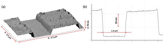
crystal thin film
This is the configuration of a thin crystal film. (Image: Anton Tarasov)
Films like this are used as active parts in optic and photonic devices, as well as in integral electronic and spintronic chips. Thin ferromagnetic films open a lot of prospects for spintronics (an area of science that provides for the creation of information storage and processing devices). Devices like this consume less electrical energy and have higher operating speed compared to traditional electronic ones.
However, to develop such devices scientists need films to be specifically shaped. It means that a template has to be applied to synthesized films, and they have to be cut according to it. To do so, scientists use etching. It can be either wet (chemical) or dry (plasma, reactive-ion, or just ion). In the course of wet etching a film is placed in liquid – an etching agent that dissolves the rest of it. Before that scientists cover the films with „masks” using photolitography to set out required configuration. Such a mask protects the desired part of the film from solving. In dry etching the same result is achieved using a gas that destroys the material physically or chemically.
„We’ve broadened the application of this approach, extended it to new iron-silicon alloys, and showed that it works. We’ve also determined the speed of etching and developed a micro-device. The same methods may be used for the production of different structures in electronics, photonics, and other applications,” said Anton Tarasov, a co-author of the article, candidate of physical and mathematical sciences, a scientific associate of Kirensky Institute of Physics (FRC KSC of SD RAS), and senior tutor at Siberian Federal University.
Scientists point out that a big advantage of the new films is not only their electronic and magnetic properties, but compatibility with the most popular technological semiconductors. It means, these films may be grown on bases made of silicon, germanium, and gallium arsenide. This will help the team obtain high-quality thin films with specific shapes and geometry in a simpler and more affordable way. Moreover, the obtained results increase the selection of materials that scientists may use to develop different devices.
„Using this technology, one can create spintronic or photonic devices, because iron silicides have properties applicable in these areas of science. Right now we are growing new films and studying the effects that depend on their topology,” concluded the scientist.
The team worked in collaboration with scientists from Siberian State Aerospace University and Lomonosov Moscow State University. The research was supported with grants from Russian Foundation for Basic Research and Krasnoyarsk Regional Science Foundation, as well as with the grant of the President of the Russian Federation for the support of leading scientific establishments.
Source: Siberian Federal University

Inginerii creează grafen în mod artificial într-o structură semiconductoră nanofabricată(Engineers create artificial graphene in a nanofabricated semiconductor structure)

Acest grafen artificial are mai multe avantaje față de grafenul natural: de exemplu, cercetătorii pot proiecta variații în grilaj de fagure pentru a modula comportamentul electronic. Și deoarece distanța dintre punctele cuantice este mult mai mare decât distanța inter-atomică în grafenul natural, cercetătorii pot observa fenomene cuantice chiar mai exotice prin aplicarea unui câmp magnetic.
Descoperirea de noi materiale cu dimensiuni reduse, cum ar fi grafenul și alte straturi superficiale, straturi van der Waals care prezintă fenomene fizice noi, care au fost anterior inaccesibile, au pus bazele acestui studiu.

Posted: Dec 12, 2017

Engineers create artificial graphene in a nanofabricated semiconductor structure

(Nanowerk News) Researchers at Columbia Engineering, experts at manipulating matter at the nanoscale, have made an important breakthrough in physics and materials science, recently reported in Nature Nanotechnology („Observation of Dirac Bands in Artificial Graphene in Small Period Nano-patterned GaAs Quantum Wells”). Working with colleagues from Princeton and Purdue Universities and Istituto Italiano di Tecnologia, the team has engineered “artificial graphene” by recreating, for the first time, the electronic structure of graphene in a semiconductor device.

“This milestone defines a new state-of-the-art in condensed matter science and nanofabrication,” says Aron Pinczuk, professor of applied physics and physics at Columbia Engineering and senior author of the study. “While artificial graphene has been demonstrated in other systems such as optical, molecular, and photonic lattices, these platforms lack the versatility and potential offered by semiconductor processing technologies. Semiconductor artificial graphene devices could be platforms to explore new types of electronic switches, transistors with superior properties, and even, perhaps, new ways of storing information based on exotic quantum mechanical states.”
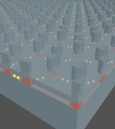
Schematic diagram of artificial graphene in a semiconductor
Schematic diagram of artificial graphene in a semiconductor. Etched pillars define the positions of quantum dots (red puddles) arranged in an hexagonal lattice. When the spacing between the quantum dots is sufficiently small, electrons can move between them. (Image: Diego Scarabelli/Columbia Engineering)
The discovery of graphene in the early 2000s generated tremendous excitement in the physics community not only because it was the first real-world realization of a true two-dimensional material but also because the unique atomic arrangement of the carbon atoms in graphene provided a platform for testing new quantum phenomena that are difficult to observe in conventional materials systems. With its unusual electronic properties¾its electrons can travel great distances before they are scattered¾graphene is an outstanding conductor. These properties also display other unique characteristics that make electrons behave as if they are relativistic particles that move close to the speed of light, conferring upon them exotic properties that “regular,” non-relativistic electrons do not have.
But graphene, a natural substance, comes in only one atomic arrangement: the positions of the atoms in the graphene lattice are fixed, and thus all experiments on graphene must adapt to those constraints. On the other hand, in artificial graphene the lattice can be engineered over a wide range of spacings and configurations, making it a holy grail of sorts for condensed matter researchers because it will have more versatile properties than the natural material.
“This is a rapidly expanding area of research, and we are uncovering new phenomena that couldn’t be accessed before,” says Shalom Wind, faculty member of the department of applied physics and applied mathematics and co-author of the study. “As we explore novel device concepts based on electrical control of artificial graphene, we can unlock the potential to expand frontiers in advanced optoelectronics and data processing.”
“This work is really a major advance in artificial graphene. Since the first theoretical prediction that system with graphene-like electronic properties may be artificially created and tuned with patterned 2D electron gas, no one had succeeded, until the Columbia work, in directly observing these characteristics in engineered semiconductor nanostructures,” says Steven G. Louie, professor of physics, University of California, Berkeley. “Previous work with molecules, atoms and photonic structures represent far less versatile and stable systems. The nanofabricated semiconductor structures open up tremendous opportunities for exploring exciting new science and practical applications.”
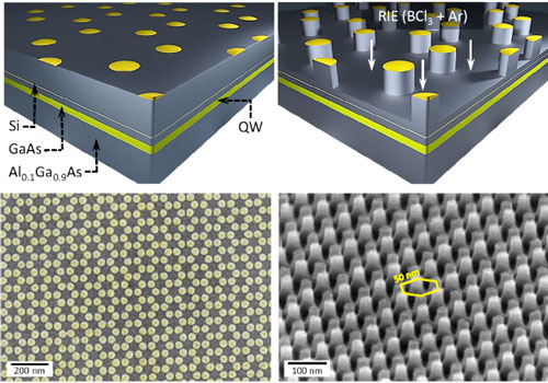
Nanofabrication of artificial graphene in a semiconductor
Nanofabrication of artificial graphene in a semiconductor. The green layer represents the 2D sheet where the electrons can move. Nanolithography and etching form small pillars beneath which lie the quantum dots arranged in an hexagonal lattice. Scanning electron micrographs at the bottom show the hexagonal array, with a period of only 50 nanometers, from the top and at an angle. (Image: Diego Scarabelli/Columbia Engineering)
The researchers used the tools of conventional chip technology to develop the artificial graphene in a standard semiconductor material, gallium arsenide. They designed a layered structure so that the electrons could move only within a very narrow layer, effectively creating a 2D sheet. They used nanolithography and etching to pattern the gallium arsenide: the patterning created a hexagonal lattice of sites in which the electrons were confined in the lateral direction. By placing these sites, which could be thought of as “artificial atoms,” sufficiently close to one another (~ 50 nanometers apart), these artificial atoms could interact quantum mechanically, similar to the way atoms share their electrons in solids.
The team probed the electronic states of the artificial lattices by shining laser light on them and measuring the light that was scattered. The scattered light showed a loss of energy that corresponded to transitions in the electron energy from one state to another. When they mapped these transitions, the team found that they were approaching zero in a linear fashion around what is called the “Dirac point” where the electron density vanishes, a hallmark of graphene.
This artificial graphene has several advantages over natural graphene: for instance, researchers can design variations into the honeycomb lattice to modulate electronic behavior. And because the spacing between the quantum dots is much larger than the inter-atomic spacing in natural graphene, researchers can observe even more exotic quantum phenomena with the application of a magnetic field.
The discovery of new low-dimensional materials, such as graphene and other ultrathin, layered van der Waals films that exhibit exciting new physical phenomena that were previously inaccessible, laid the groundwork for this study. “What was really critical to our work was the impressive advancements in nanofabrication,” Pinczuk notes. “These offer us an ever-increasing toolbox for creating a myriad of high-quality patterns at nanoscale dimensions. This is an exciting time to be a physicist working in our field.”
Source: Columbia University

Sticla cu opacitate comutativă ar putea îmbunătăți celulele solare și LED-urile(Glass with switchable opacity could improve solar cells and LEDs)

au creat sticlă care permite o cantitate mare de lumină în timp ce apare tulbure. Aceasta este prima dată când sticla a fost făcută cu un nivel ridicat de opacitate și de transmisie a luminii în același timp, o combinație de proprietăți care ar putea contribui la creșterea performanței celulelor solare și a LEDurilor.

Posted: Dec 11, 2017

Glass with switchable opacity could improve solar cells and LEDs

(Nanowerk News) Using nanoscale grass-like structures, researchers at the University of Pittsburgh, Pennsylvania have created glass that lets through a large amount of light while appearing hazy. This is the first time that glass has been made with such high levels of haze and light transmittance at the same time, a combination of properties that could help boost the performance of solar cells and LEDs.

The glass exhibits another remarkable quality: It can be switched from hazy to clear by applying water. This could make it useful for creating smart windows that change haze or opacity to control the privacy of a room or to block glare from sunlight.
„Switchable glass available today is quite expensive because it uses transparent conducting layers to apply a voltage across the entire glass,” said Paul W. Leu of the University of Pittsburgh’s Swanson School of Engineering, leader of the research team. „Our glass would be potentially less expensive to make because its opacity can be switched in a matter of seconds by simply applying or removing liquid.”
The top image shows that text can be read through normal flat glass, while the glass etched with nanostructure scatters light, making the glass appear opaque
Researchers created a new type of glass that is etched with nanograss structures. The top image shows that text can be read through normal flat glass, while the glass etched with nanostructure scatters light, making the glass appear opaque. This glass could help boost the performance of solar cells and LEDs. (Image: Sajad Haghanifar, University of Pittsburgh)
In Optica („Ultrahigh Transparency, Ultrahigh Haze Nanograss Glass with Fluid-Induced Switchable Haze”), The Optical Society’s journal for high impact research, the researchers describe their new nanograss-based glass, which achieves a record 95 percent light transmittance and a similarly high degree of haze at the same time. The researchers experimented with glass etched with nanograss structures from 0.8 to 8.5 microns in height with „blades” each measuring a few hundred nanometers in diameter.
The discovery of switchability was one of serendipity. „I was cleaning the new nanograss glass when I discovered that cleaning it with water made the glass become clear,” said project lead, graduate student Sajad Haghanifar. While the discovery was incidental, it can be easily explained. „The water goes between the extremely hydrophilic nanostructures, making the nanograss glass act like a flat substrate. Because water has a very similar index of refraction to the glass, the light goes straight through it. When the water is removed, the light hits the scattering nanostructures, making the glass appear hazy.”

Using nanograss to improve solar cells

Leu’s group developed the new glass to improve the ability of solar cells to capture light and turn it into power. Nanostructure patterns can prevent light from reflecting off the solar cell’s surface. These structures also scatter the light that enters the glass, helping more of the light reach the semiconductor material within the solar cell, where it is converted into power.
The new glass uses a unique pattern of nanostructures that looks much like grass. Because the structures are taller than previously-used nanostructures, they increase the likelihood that light will be scattered. Although glass with the nanostructures appears opaque, tests showed that most of the scattered light makes its way through the glass.
The fact that the glass is highly hazy and exhibits high transmittance could also make it useful for LEDs, which work in a way that is essentially the opposite of a solar cell, by using electricity that enters a semiconductor to produce light that is then emitted from the device. The new glass could potentially increase the amount of light that makes it from the semiconductor into the surroundings.
New glass etched with nanograss structures can be switched from hazy to clear by applying water
New glass etched with nanograss structures can be switched from hazy to clear by applying water. As shown here, removing the water from the glass makes it appear hazy again. This switchable glass could offer a simple and inexpensive way to make smart windows that change between clear and opaque. (Image: Sajad Haghanifar, University of Pittsburgh)

Finding the right ‘grass’ height

The researchers found that shorter nanograss improved the antireflection properties of the glass while longer nanograss tended to increase the haze. Glass with 4.5-micron-high nanograss showed a nice balance of 95.6 percent transmittance and 96.2 percent haze for light with a 550-nanometer wavelength (yellow light, a component of sunlight).
Although more work is needed to estimate the exact cost of manufacturing the new glass, the researchers predict that their glass will be inexpensive because it is easy to make. The nanostructures are etched into the glass using a process known as reactive ion etching, a scalable and straightforward method commonly used to make printed circuit boards.
To turn the glass into a smart window that switches from hazy to clear, it would require placing a piece of traditional glass over the nanograss glass. Pumps could be used to flow liquid into the space between the two glasses, and a fan or pump could be used to remove the water. The researchers also showed that in addition to water, applying acetone and toluene can also switch the glass from hazy to clear.
„We are now conducting durability tests on the new nanograss glass and are evaluating its self-cleaning properties,” said Haghanifar. „Self-cleaning glass is very useful because it prevents the need for robotic or manual removal of dust and debris that would reduce the efficiency of solar panels, whether the panels are on your house or on a Mars rover.”
Source: The Optical Society