Dezvoltarea de materiale avansate de grafen pentru industrie(Developing advanced graphene materials for industry)

Centrul de Cercetare al ARC pentru Transformarea Industriei prin Graphene va dezvolta produse de înaltă valoare și soluții inovatoare pentru diverse industrii precum agricultura, mineritul, construcțiile, tehnologiile medicale și apărarea.Grafenul este un singur strat de atomi de carbon care deține proprietăți de material de neegalat – este cel mai subțire, cel mai puternic, cel mai ușor material cunoscut, cu cea mai mare suprafață și cele mai bune proprietăți de conductivitate electrică și termică din orice alt material, rezistent la apă și netoxic, cu unele proprietăți anti-bacteriene

Posted: Dec 08, 2017

Developing advanced graphene materials for industry

(Nanowerk News) Research and development around new applications and industries based on the advanced material graphene is the focus of a new Graphene Research Hub being launched at the University of Adelaide today.

The ARC Research Hub for Graphene Enabled Industry Transformation will develop high-value products and innovative solutions for industries as diverse as agriculture, mining, construction, medical technologies and defence.
The Research Hub is supporting commercialisation of graphene research in a partnership between universities and industry partners. It is funded by the Australian Government through the Australian Research Council’s Industrial Transformation Research Hubs scheme with a $2.6 million grant, with industry partners contributing over $3 million.
Graphene is produced from graphite which is mined from the ground. South Australia has the largest deposit of high quality of graphite in Australia, at 200 million tonnes. Graphene has unique properties and is so thin that one gram of graphene can cover the size of a football oval.
“Graphene is a single layer of carbon atoms that holds unrivalled material properties – it’s the thinnest, strongest, lightest material known, with the greatest surface area, and the best electrical and thermal conductivity properties of any other material, as well as being flexible, water repellent and non-toxic with some anti-bacterial properties,” says Professor Dusan Losic, Director of the ARC Research Hub for Graphene Enabled Industry Transformation, which is based in the University of Adelaide’s School of Chemical Engineering.
“It has the potential for new disruptive technology that will change our lives and create new industries, the same as silicon did 60 years ago.”
The research group in Adelaide are already working on a new generation of fire retardant products, construction materials, advanced protective coatings for defence and industrial applications including slow-release fertilisers; and new electrical devices and super-batteries.
“The aim is that our research will transform industry and support Australian businesses to embrace cutting-edge innovation and technologies that deliver high-value returns and build new industries,” Professor Losic says. “We have a vision of South Australia becoming the ‘Graphene Valley’ of Australia.”
The University of Adelaide will lead the new ARC Research Hub with collaborators at Monash University, University of Melbourne and University of South Australia. The commercial partners are Archer Exploration Limited, Ziltek Pty Ltd, Qingdao Huagao Graphene Technology Corporation Limited, First Graphene Limited, and Cleanfuture Energy Australia Pty Ltd.
The Hub also has a training component with a cohort of postgraduate students and postdoctoral researchers.
Source: University of Adelaide

Nanoscienții dezvoltă noi materiale cu pori controlabile(Nanoscientists develop new material with controllable pores)

oamenii de știință descriu sintetizarea unui material nou din copolimerii de sticlă, o moleculă gigantică cu arhitectură specială. Aceste molecule au peri care emană dintr-o coloană vertebrală cu blocuri de capăt. Echipa de cercetare a prezis ca aceasta combinatie unica de componente reactive intr-o singura molecula ar forma un material puternic cu pori controlabile.

Posted: Dec 06, 2017

Nanoscientists develop new material with controllable pores

(Nanowerk News) What do your skin, the clothes you wear, and the soil you stand on have in common? They are all porous substances. Like a sponge, their surfaces are covered with tiny holes that allow liquids and gasses to pass through. Porous materials are widespread throughout our world, and those with nanoscale pores—called mesoporous materials—make up everything from chemical catalyst supports to gas storage chambers and separation membranes.

To date, scientists have struggled to fabricate strong mesoporous materials; however, they have successfully developed “microporous” materials. These materials have even smaller pores, measuring less than two nanometers. Scientists construct these incredibly tiny materials using the “molecular framework” concept, where small, rigid molecules are interconnected to generate a continuous structure. While a lack of suitable building blocks in the mesoporous regime (two to 50 nanometers) has prevented scientists from developing strong mesoporous materials, a research team at the University at Buffalo (UB) has now solved this problem.
“Once you get to a certain size, most molecules become too flexible and aren’t strong enough to maintain a material’s pore framework,” said Dmytro Nykypanchuk, a scientist at the Center for Functional Nanomaterials (CFN)—a U.S. Department of Energy Office of Science User Facility located at Brookhaven National Laboratory. “This has led the scientists at UB to develop an entirely new approach to the synthesis of mesoporous materials.”
special architecture of bottlebrush copolymers
This image depicts the special architecture of bottlebrush copolymers (top left), which have bristles that emanate from a backbone with end blocks. By interconnecting these molecules, scientists fabricated a mesoporous material (right).
In a paper published in ACS Nano („Mesoporous Polymer Frameworks from End-Reactive Bottlebrush Copolymers”), the scientists describe synthesizing a new material from bottlebrush copolymers, a giant molecule with special architecture. These molecules have bristles that emanate from a backbone with end blocks. The research team predicted this unique combination of reactive components in a single molecule would form a strong material with controllable pores. Specifically, the side chains could serve as extra rigid interconnectors, while the reactive end blocks could help multiple bottlebrush molecules bind together.
“Bottlebrush copolymers provide a unique platform for fabricating mesoporous materials,” said Javid Rzayev, the lead researcher of the project and a chemistry professor at UB. “By manipulating their molecular architecture, we can control the molecular rigidity and the directionality of intermolecular interactions. This has allowed us to develop a mesoporous material with molecularly tunable parameters.”
To confirm their results, the UB research team analyzed the new material’s structure at the National Synchrotron Light Source II (NSLS-II), also a DOE Office of Science User Facility. Using a technique called small angle x-ray scattering, the team directed the bright x-rays from beamline 11-BM—a beamline built in a partnership between NSLS-II and CFN—to observe how light bounces off the atoms within the material. The study revealed the new material was far different than those produced by traditional methods. Because each pore was constructed by several macromolecules, the newly developed material had a much larger number of pores per volume, while the pores exhibited uniform dimensions and maintained their rigidity. Most importantly, the scientists could control the pores by manipulating the structure of the bottlebrush copolymers.
“Because the pores are defined by molecular architecture, scientists have far more control over the pore size and the properties of these materials than they did before,” Nykypanchuk said.
With a sturdy and controllable framework to work off, scientists can now research ways to improve mesoporous materials, such as altering the nature of the pores to make them catalytically active.
Source: Brookhaven National Laboratory

Grâul devine impresionat din nanotuburi purificate(Wheat gets boost from purified nanotubes)

Nanotuburile de carbon purificate cu un singur perete dispersate în apă au promovat o creștere mai mare a plantelor (centru) decât controlul fără nanomateriale (stânga) după opt zile;dacă nanotuburile cu pereți unici se combină cu poluanți organici, cum ar fi pesticidele, substanțele chimice industriale sau solvenții din mediu, aceștia pot concentra și imobiliza toxinele și pot spori absorbția acestora de către plante.

Posted: Dec 06, 2017

Wheat gets boost from purified nanotubes

(Nanowerk News) The introduction of purified carbon nanotubes appears to have a beneficial effect on the early growth of wheatgrass, according to Rice University scientists. But in the presence of contaminants, those same nanotubes could do great harm.

The Rice lab of chemist Andrew Barron grew wheatgrass in a hydroponic garden to test the potential toxicity of nanoparticles on the plant. To their surprise, they found one type of particle dispersed in water helped the plant grow bigger and faster.
They suspect the results spring from nanotubes’ natural hydrophobic (water-avoiding) nature that in one experiment apparently facilitated the plants’ enhanced uptake of water.
The research appears in the Royal Society of Chemistry journal Environmental Science: Nano(„Effect of raw and purified carbon nanotubes and iron oxide nanoparticles on the growth of wheatgrass prepared from the cotyledons of common wheat (triticum aestivum)”).
Purified single-walled carbon nanotubes dispersed in water promoted greater plant growth
Purified single-walled carbon nanotubes dispersed in water promoted greater plant growth (center) than the nanomaterial-free control (left) after eight days of an experiment at Rice University. Feeding plants tetrahydrofuran with the nanotubes (right) produced the opposite effect, stunting plant growth. (Image: Pavan Raja/Rice University)
The lab mounted the small-scale study with the knowledge that the industrial production of nanotubes will inevitably lead to their wider dispersal in the environment. The study cited rapid growth in the market for nanoparticles in drugs, cosmetic, fabrics, water filters and military weapons, with thousands of tons produced annually.
Despite their widespread use, Barron said few researchers have looked at the impact of environmental nanoparticles – whether natural or man-made – on plant growth.
The researchers planted wheatgrass seeds in multiple replicates in cotton wool and fed them with dispersions that contained raw single-walled or multi-walled nanotubes, purified single-walled nanotubes or iron oxide nanoparticles that mimicked leftover catalyst often attached to nanotubes. The solutions were either water or tetrahydrofuran (THF), an industrial solvent. Some of the seeds were fed pure water or THF as a control.
After eight days, the plantings showed that purified single-walled nanotubes in water enhanced the germination rate and shoot growth of wheatgrass, which grew an average of 13 percent larger than plants in plain water. Raw single- and multi-walled nanotubes and particles in either solution had little effect on the plants’ growth, they found.
However, purified single-walled nanotubes in THF retarded plant development by 45 percent compared to single-walled nanotubes in water, suggesting the nanotubes act as a carrier for the toxic substance.
The concern, Barron said, is that if single-walled nanotubes combine with organic pollutants like pesticides, industrial chemicals or solvents in the environment, they may concentrate and immobilize the toxins and enhance their uptake by plants.
Nothing seen in the limited study indicated whether carbon nanotubes in the environment, and potentially in plants, will rise up the food chain and be harmful to humans, he said.
On the other hand, the researchers said it may be worth looking at whether hydrophobic substrates that mimic the positive effects observed in single-walled nanotubes could be used for high-efficiency channeling of water to seeds.
„Our work confirms the importance of thinking of nanomaterials as part of a system rather in isolation,” Barron said. „It is the combination with other compounds that is important to understand.”
Source: Rice University

The world’s smallest Mona Lisa(The world’s smallest Mona Lisa)

profesor asistent de bioinginerie la Caltech, au dezvoltat o metoda ieftina prin care ADN-ul origami se auto-asambleaza in mese mari, cu modele personalizabile in intregime, creand un fel de panza care poate afisa orice imagine;Folosind acest instrument software online și tehnici automate de manipulare a lichidelor, mai multe alte modele au fost proiectate și asamblate din fire de ADN, incluzând un portret de viață al unei bacterii și un portret de dimensiuni bacteriene al unui cocoș.;fabricarea materialelor avansate sau studierea interacțiunilor dintre substanțe chimice sau biomolecule”

Posted: Dec 06, 2017

The world’s smallest Mona Lisa

(Nanowerk News) In 2006, Caltech’s Paul Rothemund (BS ’94) – now research professor of bioengineering, computing and mathematical sciences, and computation and neural systems – developed a method to fold a long strand of DNA into a prescribed shape. The technique, dubbed DNA origami, enabled scientists to create self-assembling DNA structures that could carry any specified pattern, such as a 100-nanometer-wide smiley face.

DNA origami revolutionized the field of nanotechnology, opening up possibilities of building tiny molecular devices or „smart” programmable materials. However, some of these applications require much larger DNA origami structures.
Now, scientists in the laboratory of Lulu Qian, assistant professor of bioengineering at Caltech, have developed an inexpensive method by which DNA origami self-assembles into large arrays with entirely customizable patterns, creating a sort of canvas that can display any image. To demonstrate this, the team created the world’s smallest recreation of Leonardo da Vinci’s Mona Lisa – out of DNA.
DNA rendering of the Mona Lisa viewed with atomic force microscopy
DNA rendering of the Mona Lisa viewed with atomic force microscopy. (Image: Qian laboratory)
The work is described in a paper appearing in the December 7 issue of the journal Nature(„Fractal assembly of micrometre-scale DNA origami arrays with arbitrary patterns”).
While DNA is perhaps best known for encoding the genetic information of living things, the molecule is also an excellent chemical building block. A single-stranded DNA molecule is composed of smaller molecules called nucleotides–abbreviated A, T, C, and G–arranged in a string, or sequence. The nucleotides in a single-stranded DNA molecule can bond with those of another single strand to form double-stranded DNA, but the nucleotides bind only in very specific ways: an A nucleotide with a T or a C nucleotide with a G. These strict base-pairing „rules” make it possible to design DNA origami.
To make a single square of DNA origami, one just needs a long single strand of DNA and many shorter single strands–called staples–designed to bind to multiple designated places on the long strand. When the short staples and the long strand are combined in a test tube, the staples pull regions of the long strand together, causing it to fold over itself into the desired shape. A large DNA canvas is assembled out of many smaller square origami tiles, like putting together a puzzle. Molecules can be selectively attached to the staples in order to create a raised pattern that can be seen using atomic force microscopy.
The Caltech team developed software that can take an image such as the Mona Lisa, divide it up into small square sections, and determine the DNA sequences needed to make up those squares. Next, their challenge was to get those sections to self-assemble into a superstructure that recreates the Mona Lisa.
„We could make each tile with unique edge staples so that they could only bind to certain other tiles and self-assemble into a unique position in the superstructure,” explains Grigory Tikhomirov, senior postdoctoral scholar and the paper’s lead author, „but then we would have to have hundreds of unique edges, which would be not only very difficult to design but also extremely expensive to synthesize. We wanted to only use a small number of different edge staples but still get all the tiles in the right places.”
The key to doing this was to assemble the tiles in stages, like assembling small regions of a puzzle and then assembling those to make larger regions before finally putting the larger regions together to make the completed puzzle. Each mini puzzle utilizes the same four edges, but because these puzzles are assembled separately, there is no risk, for example, of a corner tile attaching in the wrong corner. The team has called the method „fractal assembly” because the same set of assembly rules is applied at different scales.
„Once we have synthesized each individual tile, we place each one into its own test tube for a total of 64 tubes,” says Philip Petersen, a graduate student and co-first author on the paper. „We know exactly which tiles are in which tubes, so we know how to combine them to assemble the final product. First, we combine the contents of four particular tubes together until we get 16 two-by-two squares. Then those are combined in a certain way to get four tubes each with a four-by-four square. And then the final four tubes are combined to create one large, eight-by-eight square composed of 64 tiles. We design the edges of each tile so that we know exactly how they will combine.”
The Qian team’s final structure was 64 times larger than the original DNA origami structure designed by Rothemund in 2006. Remarkably, thanks to the recycling of the same edge interactions, the number of different DNA strands required for the assembly of this DNA superstructure was about the same as for Rothemund’s original origami. This should make the new method similarly affordable, according to Qian.
„The hierarchical nature of our approach allows using only a small and constant set of unique building blocks, in this case DNA strands with unique sequences, to build structures with increasing sizes and, in principle, an unlimited number of different paintings,” says Tikhomirov. „This economical approach of building more with less is similar to how our bodies are built. All our cells have the same genome and are built using the same set of building blocks, such as amino acids, carbohydrates, and lipids. However, via varying gene expression, each cell uses the same building blocks to build different machinery, for example, muscle cells and cells in the retina.”
The team also created software to enable scientists everywhere to create DNA nanostructures using fractal assembly.
„To make our technique readily accessible to other researchers who are interested in exploring applications using micrometer-scale flat DNA nanostructures, we developed an online software tool that converts the user’s desired image to DNA strands and wet-lab protocols,” says Qian. „The protocol can be directly read by a liquid-handling robot to automatically mix the DNA strands together. The DNA nanostructure can be assembled effortlessly.”
Using this online software tool and automatic liquid-handling techniques, several other patterns were designed and assembled from DNA strands, including a life-sized portrait of a bacterium and a bacterium-sized portrait of a rooster.
„Other researchers have previously worked on attaching diverse molecules such as polymers, proteins, and nanoparticles to much smaller DNA canvases for the purpose of building electronic circuits with tiny features, fabricating advanced materials, or studying the interactions between chemicals or biomolecules,” says Petersen. „Our work gives them an even larger canvas to draw upon.”
Source: California Institute of Technology

Curentul monopole oferă un mod de a controla magneții(Monopole current offers way to control magnets)

au descoperit noi proprietăți magnetice interesante ale unui tip de material cunoscut sub numele de ” cu gheață de spin quantum. ”
Aceste materiale prezintă proprietăți interesante deoarece se comportă ca „magneți frustrați” – sisteme care se pot regla în diferite stări magnetice din cauza geometriei lor speciale. O proprietate importantă a acestor materiale este aceea că au monopoluri virtuale – particule care sunt fie nordice sau sudice, dar nu ca niște magneți tipici, care au în mod invariabil atât un pol de nord cât și un sud limitat împreună.

Posted: Dec 01, 2017

Monopole current offers way to control magnets

(Nanowerk News) In work published in Physical Review Letters („Quantum Spin Ice under a [111] Magnetic Field: From Pyrochlore to Kagome”), scientists from RIKEN in Japan have discovered interesting new magnetic properties of a type of materials known as „quantum spin ice.”

These materials demonstrate interesting properties as they behave as „frustrated magnets”–systems that can settle into various magnetic states because of their special geometry. One important property of these materials is that they have virtual monopoles–particles that are either north or south but not like typical magnets, which invariably have both a north and south pole confined together.
Using numerical simulations, the group showed how a magnetic field could be used to control the properties of north and south poles, which are fractionalized from magnetic moments of electrons, on a frustrated magnet called a quantum spin ice.
The group first proposed a model for quantum spin ice–spin ice based on quantum properties–in 2010 in order to describe the low-energy magnetic properties of magnetic rare-earth pyrochlores–a type of mineral that show interesting physical properties. In 2012, experiments showed that this model was valid. This system includes a quantum spin liquid state where spins–the property of electrons that lead to magnetic properties–are prevented from ordering and freezing by zero-point motion, a type of motion allowed even at zero temperature under quantum mechanics, of their monopoles.
Since monopole charges are subject to a conservation law, the motion of north and south poles directly affects the direction of magnetic moments in the system. In addition, electric charges are not carried by these monopoles, and thus the monopole current is not accompanied by an electric current that would lead to a large energy loss through Joule heat. „Because of this,” says Shigeki Onoda, the leader of the group, „monopole current offers a potentially efficient way of controlling magnets without loss.”
Through this work, the researchers revealed that there are successive transitions from the quantum spin liquid state if a magnetic field is applied in a special direction along which kagome-lattice layers and triangular-lattice layers are stacked one on top of the other.
First, the magnetization of the system rises smoothly to a value two-third of the maximum value in the quantum spin liquid state, and then remains at that level in a finite range of the field strength, which is called the 2/3 magnetization plateau. In this plateau state, the zero-point motion of monopoles are spatially confined and localized, and thus this state cannot host a coherent monopole current.
However, as the strength of the magnetic field is increased, the magnetization of the material eventually begins to rise again and concomitantly, the monopole charges become disproportionate and show a superfluidity. This is a magnetic analogue of a supersolid in helium 4, where the atoms show both a non-uniform spatial distribution and a superfluidity, which supports frictionless and thus dissipationless current, at extremely low temperature. The monopole supersolid phase survives until the magnetization saturates to the maximum value.
According to Onoda, „Our work indicates that the conductivity associated with the monopole current can be substantially controlled by applying a magnetic field to quantum spin ice and that it is possible to host dissipationless monopole current in the monopole supersolid phase. Our findings may also open a novel route to the efficient control of magnetism for a range of potential applications such as memory devices.”
Source: RIKEN

Eliminarea ecologică a biocombustibililor cu nanocoate(Environmentally-friendly removal of biofouling with nanocoatings)

Aceasta înseamnă că vopseaua rezistentă la coroziune durează mai mult timp și mușchii pot fi curățați rapid și ușor”, explică dr. Martina Baum, biolog tehnician de la grupul de lucru al profesorului Rainer Adelung, funcțional Nanomateriale, unde se află ideea inițială acoperirea a apărut acum câțiva ani

Posted: Dec 01, 2017

Environmentally-friendly removal of biofouling with nanocoatings

(Nanowerk News) It is one of the shipping industry’s major problems: marine organisms like barnacles, algae or muscles quickly cover the hulls of ships and damage their paintwork. The phenomenon of so-called „biofouling” increases the ship’s weight and its flow resistance, causing greater fuel consumption and CO2 emissions. In order to avoid this growth, protective paints are mainly used around the world which contain and release pollutants.

A research team at Kiel University and the Phi-Stone AG, one of its spin-offs located in Kiel, have closely cooperated to develop an environmentally-friendly coating. This coating makes it harder for marine organisms to grow on the hulls and makes cleaning the ships easier. The new approach has now been awarded an international prize for innovative marine technology and beat competitors from three continents.
barnacles attached to a ship's hull
A major problem for ships: organisms like barnacles attach themselves to their surfaces, cause damage and also increase their fuel consumption. (Image: HP Voiß)
„This project from the field of nanotechnology is a great example of transferring innovation from Schleswig-Holstein, whereby findings from basic research are brought into industrial application. We, as a university, want to solve existing problems using innovative ideas. In order to do so, this requires a working dialogue between science and companies,” stressed Professor Karin Schwarz, Vice President of technology transfer at Kiel University.

Around 40 percent higher fuel consumption due to biofouling

„We estimate that biofouling increases the amount of fuel ships use by up to 40 percent. This costs the world’s transport industry over 150 billion US dollars per year and causes unnecessary environmental pollution,” added Ingo Paulowicz, Board Member of Phi-Stone, a spin-off from Kiel University.
On top of that, cleaning and maintenance increases considerably, in terms of removing the barnacles and other organisms attached to the hulls and repainting. Many of the existing protective paints have already been forbidden due to their massive polluting effects. This includes organotin paints like TBT (tributyltin). Copper-based compounds are expected to be prohibited next year, which will drastically increase the need for environmentally-friendly and long-lasting coatings for ships.

Longer-lasting and more environmentally-friendly

The coating developed in close collaboration by the scientists from Kiel University and Phi-Stone is both environmentally-friendly and long-lasting. The product requires no solvents and does not release any pollutants into the sea – unlike the widespread self-polishing coatings which contain copper. These are gradually removed when the ship moves through the water and continuously release poisonous substances. The smooth surface of the new coating developed in Kiel makes it harder for organisms to attach themselves to the hulls and destroy the paintwork.
„This means that the bio-corrosion-resistant paint lasts longer and barnacles or muscles can be brushed off quickly and easily,” explains Dr Martina Baum, technical biologist from Professor Rainer Adelung’s Functional Nanomaterials working group, which is where the original idea for the coating arose several years ago.
applying a nanocoating to a ship's hull
The new coating has already been successfully tested on ships like the ‘African Forest’. Technical biologist from Kiel University, Dr Martina Baum, applied the test coating herself. (Image: CAU)
Together with her then-doctoral researcher, materials scientist Iris Hölken, Baum investigated the growth-reduction properties of a polymer composite, which was based on polythiourethane (PTU) and specially-formed ceramic particles. They improve the mechanical properties of the coating and the ability of the paint to adhere to the surface of the ship. Together with Phi-Stone AG, they further developed the material and the coating process.
„Every year around the world, 80,000 tonnes of so-called anti-fouling paints are now being used. This costs around 4 billion dollars per annum. Not to mention the cost to the oceans,” says Phi-Stone Board Member Paulowicz, to emphasise the scale of environmentally-friendly alternatives.

Successful technology transfer through collaboration between Kiel University and Phi-Stone AG

The research team from Kiel University and Phi-Stone AG tested the new product with companies based in Schleswig-Holstein, initially on ships in the water tanks at the GEOMAR Helmholtz Centre for Ocean Research Kiel.
„These tests went very well,” said Baum. „We were able to determine significantly less growth after two years on the ‘African Forest’, which travels from Belgium to Gabon in central Africa. This was then easy to clean off with a plain sponge.” Dr Iris Hölken, who has now completed her doctoral studies, is continuing with this topic as the scientific head of the project at Phi-Stone. The company is currently working on developing a spraying technique, with which the coating can be applied easily and over large areas.

International award for innovative marine technology from Kiel

Phi-Stone AG, the spin-off from Kiel University, won the Global Marine Technology Entrepreneurship Competition in November, with its environmentally-friendly coating for ships. A total of 120 teams took part in the qualifying rounds in Paris, London, Shanghai or at the Massachusetts Institute of Technology in Boston.
The German qualifying round took place in Kiel at the end of October: Ingo Paulowicz, Board Member of Phi-Stone, and staff member Haoyi Qiu, who is also completing a doctoral degree at Kiel University, successfully presented their environmentally-friendly coating concept at the GEOMAR Helmholtz Centre for Ocean Research Kiel. In the finals in Qingdao, in China, they beat the strong competitors from three continents.
The competition, which is organised by Shandong University and the city of Qingdao, aims to promote innovative marine technology and open up contacts to the Chinese market. The first prize is 70,000 US dollars and includes additional funding measures on site.
„We are extremely pleased to have won such a major global competition on maritime innovation,” says Paulowicz, who was also a Kiel University graduate. „We definitely want to keep our company in Schleswig-Holstein, but are excited about the extra possibilities that the Chinese market can offer us.”
„It’s great that this idea was developed in exchange with companies and that we were thus able to transfer it from the lab to the ship,” says Professor Rainer Adelung, head of the working group at Kiel University, who is also very pleased about this success. „It is a great achievement for us as a university, but also for the state, if ideas from Schleswig-Holstein are also convincing at the international level in this way.”
Source: Kiel University

ALON Transparențe ceramice optice pentru aplicații senzor și armură(ALON Optical Ceramic Transparencies for Sensor and Armor Applications)

Cea mai mare cerere și oportunitate continuă să fie în domeniul armelor transparente, totuși, piața ferestrelor de recunoaștere și a cuptoarelor / ferestrelor senzoriale, realizate de la ALON, continuă să crească și la o rată impresionantă;cantitățile foarte mari de materiale cerute de piața blindată transparentă beneficiază, de asemenea, pe piața senzorilor;Azotul stabilizează structura de cristal spinel cubic pe o gamă largă de compoziție

stimp26

Cerneluri cu semiconductoare ecologice, care utilizează surfactanți(Eco-friendly waterborne semiconductor inks using surfactant)

a dezvoltat o tehnologie pentru a produce cerneluri semiconductoare pe bază de apă ecologice folosind surfactant, aditivi care amestecă substanțe de diferite proprietăți și componentă a săpunului.
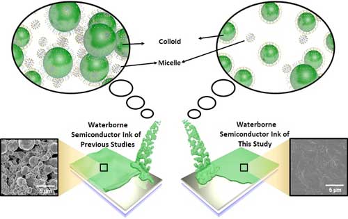
Semiconductorii polimeri sunt compuși ai carbonului care prezintă proprietățile electrice ale semiconductorilor. Acesta a fost evidențiat ca un material de generație următoare de dispozitive inteligente pentru uzură etc., nu numai pentru că sunt flexibile și ușoare în greutate, dar pot fi prelucrate într-o zonă extinsă și cu un cost redus prin procesul de soluționare. Cu toate acestea, există o problemă care cauzează o poluare semnificativă a mediului, deoarece solvenții organici toxici sunt utilizați în acest proces;a produs cerneluri semiconductoare cu apă; cerneala semiconductoare pe bază de apă recent dezvoltată are particule coloidale mici și miceluri surfactante comparativ la cernelurile semiconductoare pe bază de apă în studiile anterioare.

Posted: Nov 27, 2017

Eco-friendly waterborne semiconductor inks using surfactant

(Nanowerk News) A research team of Energy Science and Engineering at Daegu Gyeongbuk Institute of Science and Technology (DGIST) has developed a technology to produce environmentally friendly water-borne semiconductor inks using surfactant, which is additives that mix substances of different properties and a component of soap.

Polymer semiconductors are carbon compounds showing the electrical properties of semiconductors. It has been highlighted as a next-generation material of wearable smart devices, etc. not only because they are flexible and light in weight, but also they can be processed in a wide area a low cost through the solution process. However, there is an issue that it causes significant environmental pollution as toxic organic solvents are used in the process.
Despite the limitations, the research team has developed a semiconductor surface control technique using surfactants for environmentally friendly semiconductor manufacturing processes that do not use toxic organic solvents and has produced water-borne semiconductor inks.
a comparison of waterborne semiconductor inks
A comparison of the waterborne semiconductor ink of this study and that of the previous studies. (Image: DGIST)
In the study (Energy & Environmental Science, „Universal selection rule for surfactants used in miniemulsion processes for eco-friendly and high performance polymer semiconductors”), the newly developed waterborne semiconductor ink of the research team has small colloidal particles and less surfactant micelles compared to the waterborne semiconductor inks in the previous studies. As a result, it has a relatively flat surface than the conventional waterborne semiconductor inks. The black and white image in the figure shows the comparison of the surface of the thin film made with the waterborne semiconductor ink developed in this study and conventional one.
According to the research team, the technique is expected to be applied in various electronic devices such as P-type and N-type transistors as well as PN diodes, complementary inverters, photodiodes as high-quality thin films.
Professor Chung stressed the significance of the study by stating „This research has fundamentally solved the environmental pollution problem generated during the production of organic semiconductor, which is spotlighted as the core material of wearable electronic devices. We have developed a source technology that can disperse various semiconductor materials into water through the simple chemical modification. We expect that it can be used in various optoelectronic devices ranging from transistors to solar cell, composite circuit, and image sensor.”
Source: Daegu Gyeongbuk Institute of Science and Technology (DGIST)

Comunicarea la viteza luminii cu grafen(Communicating at the speed of light with graphene)

mesaje cu viteza luminii.
Materialele subțiri din două dimensiuni, realizate prin strat atomic de strat atomic, pot permite comunicații la o viteză mai mare și consumuri de energie mai mici decât cele realizate anterior.Acestea ar putea fi baza sistemelor optice de interconectare de generație viitoare în infrastructurile Air Force, a spus ea.

Posted: Nov 22, 2017

Communicating at the speed of light with graphene

(Nanowerk News) Imagine how much we could accomplish in a day if we could exchange messages at the speed of light.

Thin two-dimensional materials, made atomic layer by atomic layer, may enable communications at higher speed and lower power consumptions than previously realized. Multidisciplinary research in this field is happening now at the University of Delaware.
Tingyi Gu, assistant professor of electrical and computer engineering at the University of Delaware
Tingyi Gu, assistant professor of electrical and computer engineering at the University of Delaware.
For this work, Tingyi Gu, an assistant professor in the Department of Electrical and Computer Engineering, is one of 43 scientists nationwide to receive a grant this year through the Air Force Office of Scientific Research (AFOSR) Young Investigator Program this year.

The AFOSR Young Investigator Program was established to foster creative basic research. It is awarded to scholars with exceptional ability and promise who have earned their doctoral degrees within the last five years.

Under this three-year, $450,000 grant, Gu is developing „next-generation hybrid optical communications”–small, lightweight devices for efficient light generation and transportation, enabling high speed and low power optical interconnects, which is an interface between electronic signals in computers and optical fiber communication signals.

In optical communications, signals are transmitted via light. Fiber communication is the backbone bundling all the signals.
In contrast, the communications devices you use everyday, like laptops and phones, use wireless radio signals to transmit signals.
To build devices for optical communications, Gu first uses software to design the devices, optimizing their optical, electronic and thermal properties. Then, she will work with the team at the UD Nanofabrication Facility to make the devices.
„The UD Nanofabrication Facility team is actively working with Prof. Gu’s group on this project and we have recently made promising progress on fabricating those high quality nanophotonic devices on a large scale,” said Iulian Codreanu, Ph.D., director of operations at UD NanoFab.
The devices start with silicon, a material commonly used in photonics–the study of light and its applications. Then graphene, a two-dimensional material made from a single layer of atoms, is bonded onto silicon chips. Graphene can improve chip performance, including generation, amplification, modulation, and detection of optical signals.
„Its unique structure gives it unique electronic properties not enabled by bulk materials,” said Gu.
In 2010, the pioneers of graphene research, located at the University of Manchester, won the Nobel Prize in Physics. Since then, „two-dimensional materials have been a hot area of research,” said Gu.
Gu isn’t just making devices–she is testing them in order to improve speed, performance, and scalability of devices made with these materials. These could be the basis of next-generation optical interconnect systems in Air Force infrastructures, she said.
„Together we are doing very sharp engineering in combination with hot science,” said Gu. „This grant gives me more opportunity to tap the potential of my research.”
Gu’s students will also benefit from this award.
„This is a wonderful opportunity for students to get trained to understand the process from beginning to end,” she said, „which is critical for their future careers.”
Gu’s work with photonic devices has also garnered attention from NASA, which granted her an Early Career Faculty Award earlier this year.
Dennis Prather, Engineering Alumni Professor in the Department of Electrical and Computer Engineering and Dr. Gu’s faculty mentor, has been studying silicon photonics for nearly two decades. He is impressed by Gu’s success thus far.
„I’m certain she will be a future pillar of our department and I’m already so proud to call her my colleague,” he said.
Source: By Julie Stewart, University of Delaware

Un material feromagnetic cu proprietăți promițătoare(A ferromagnetic material with promising properties)

Producerea de nanoparticule din semiconductori feromagnetici cum ar fi oxidul de Europium (II) constituie o provocare imensă, mai ales în ceea ce privește geometria anizotropică. Până la urmă, particulele cu proprietăți noi interesante așteptate trebuie să fie și anizotropice;Un material inteligent cu o varietate de proprietăți”, spune Bastian Trepka de oxid de Europium (II). Mai presus de toate, are o structură cristalină simplă. „Putem explica schimbările în proprietățile cu recurs la structurile cristaline, care sunt predeterminate”În plus, cercetătorii au reușit să demonstreze că proprietățile magnetice ale oxidului de Europium (II) semiconductor sunt de fapt legate de forma nanostructurii sale sau anizotropia

Posted: Nov 21, 2017

A ferromagnetic material with promising properties

(Nanowerk News) Ferromagnetic semiconductors have attracted increasing attention over the last decade. Their properties make them promising functional materials that can be used in the field of spin-based electronics (spintronics). Spintronics is of crucial importance for the storage and transport of information. In an interdisciplinary collaboration, researchers at the University of Konstanz successfully developed a method for synthesising Europium(II) oxide (EuO) nanoparticles, a ferromagnetic semiconductor with extremely promising properties. The researchers also demonstrated that the nanoparticles have magnetic properties because of their structure.

The results of the joint research project have been published in Advanced Materials(„Nanomorphology Effects in Semiconductors with Native Ferromagnetism: Hierarchical Europium (II) Oxide Tubes Prepared via a Topotactic Nanostructure Transition”).
Picture of a hybrid particle taken by a transmission electron microscope
Picture of a hybrid particle taken by a transmission electron microscope. Pictured are the inorganic (dark) and organic (light) lamellas that the particle is made of, as well as the tubular shapes (the low-contrast area in the middle). Through vaporisation with Europium, the hybrid stage can be transformed into pure EuO. (Image: University of Konstanz)
The collaboration of the research groups led by Professor Sebastian Polarz (inorganic chemistry), Professor Mikhail Fonin (experimental physics) and Professor Ulrich Nowak (theoretical physics) from the University of Konstanz, as well as the electron microscopy team of the Leibniz Institute for Solid State and Materials Research Dresden (IFW Dresden) headed by Dr Axel Lubk, was carried out within the framework of the University of Konstanz’s Collaborative Research Centre (SFB) “Anisotropic Particles as Building Blocks: Tailoring Shape, Interactions and Structures”. “Without the cooperation of these research teams, we could not have achieved these results”, says Bastian Trepka, lead author of the study and a member of Sebastian Polarz’s research team Functional Inorganic Materials, where the nanoparticles have been synthesized.
The properties of anisotropic and magnetic nanoparticles are at the centre of the research project A5 of the SFB. Anisotropic means that the shape and the magnetic, optical or electronic properties are not identical for all spatial directions of the particle. This in turn makes it possible to investigate not only the new and often improved properties of nano-structured materials, but also the additional properties caused by anisotropy.
Producing nanoparticles from ferromagnetic semiconductors such as Europium(II) oxide constitutes a huge challenge, especially in anisotropic geometry. After all, the particles with the expected new interesting properties are to be anisotropic, too. “The aim is to deepen our understanding so that we can modulate and access the properties of nano-systems on demand”, says lead author Trepka. Using their special method, the researchers succeeded in producing high-quality and anisotropic EuO-nanoparticles that can be used to observe structure property effects.
The method is based on a two-stage process. In a first step, a hybrid material consisting of organic and inorganic components is produced, which is already anisotropic. In the next step, the hybrid material is treated with europium vapour. As a result, it chemically converts to EuO. In this case the nanoparticles’ shape is tubular. “This method is interesting because it is not limited to tubular forms. It is also possible to produce rods”, explains Bastian Trepka.
Furthermore, the researchers were able to demonstrate that the magnetic properties of the semiconductor Europium(II) oxide are actually related to the shape of its nanostructure, or rather the anisotropy. After further treatment while trying to generate counter-evidence, the tubular shapes disappeared, resulting in different properties. “The experimental physicists carried out measurements that confirmed the results that had been simulated by the theoretical physicists. This enabled us to develop ideas as to how the structure brings about this particular magnetic behaviour”, explains Bastian Trepka.
“What is really special about our process is the separation of structure control and chemical transformation. We can obtain different shapes from the same material by influencing the shape through process control. This way we will always get the material to assume the shape we need”, says Trepka. In the case of Europium(II) oxide, this is a topotactic nanotransformation that maintains its crystalline direction: it is tubular both before and after treatment.
“An intelligent material with a variety of properties”, says Bastian Trepka of Europium(II) oxide. Above all, it has a simple crystalline structure. “We can explain changes in properties with appeal to the crystalline structures, which are pre-determined”. This is ideal for basic research.
Source: University of Konstanz