Cercetătorii îmbunătățesc procesul de fabricare a nanostructurilor pentru dispozitivele electronice(Researchers improve fabrication process of nanostructures for electronic devices)

Indium-galiu-fosfid este unul din mai multe materiale testate pentru a completa siliciul ca mijloc de imbunatatire a capacitatii curente de prelucrare a semiconductoarelor.
„Acesta este un material foarte bine cunoscut și are aplicații în industria electronică și în celulele solare”, a spus el. „Nu inventăm din nou roata; noi stabilim noi protocoale pentru tratarea materialelor existente, care sunt mai rentabile și un proces mai durabil „.
Dispozitivele semiconductoare sunt create pe plachete printr-un proces în mai multe etape pentru acoperirea, îndepărtarea sau modelarea materialelor conductive. Procesele tradiționale sunt etchul umed, unde o probă cu aspecte blocate este imersată într-o baie acidă pentru îndepărtarea substanțelor și o gravare cu ioni reactivi, unde ionii bombardează suprafețele expuse pe placă pentru a-și schimba proprietățile chimice și a elimina materialele din aceste zone expuse. Ambele au fost utilizate pentru a dezvolta modelele complexe electronice pe circuite și pentru a folosi siliciul ca fundație pentru acest tip de modelare. Îmbunătățirea metodelor de modelare de către I-MacEtch ar putea însemna reducerea complexității fabricării diferitelor dispozitive fotonice și electronice.

Posted: Mar 20, 2018

Researchers improve fabrication process of nanostructures for electronic devices

(Nanowerk News) Researchers at RIT have found a more efficient fabricating process to produce semiconductors used in today’s electronic devices. They also confirmed that materials other than silicon can be used successfully in the development process that could increase performance of electronic devices. This fabrication process—the I-MacEtch, or inverse metal-assisted chemical etching method—can help meet the growing demand for more powerful and reliable nano-technologies needed for solar cells, smartphones, telecommunications grids and new applications in photonics and quantum computing.

“What is novel about our work is that for the first time we are looking at applying I-MacEtch processing to indium-gallium-phosphide materials. I-MacEtch is an alternative to two conventional approaches and is a technique that has been used in the field—but the materials that have been explored are fairly limited,” said Parsian Mohseni, assistant professor of microsystems engineering in RIT’s Kate Gleason College of Engineering. He is also director of the EINS Laboratory at the university.
Au-assisted and inverse-progression MacEtch (I-MacEtch) of the heteroepitaxial In0.49Ga0.51P/GaAs material system
Au-assisted and inverse-progression MacEtch (I-MacEtch) of the heteroepitaxial In0.49Ga0.51P/GaAs material system. (© ACS)
Demands for improved computer processing power have led researchers to explore both new processes and other materials beyond silicon to produce electronic components, Mohseni explained. The I-MacEtch process combines the benefits of two traditional methods—wet etching and reactive ion etching, or REI. Indium-gallium-phosphide is one of several materials being tested to complement silicon as a means to improve current capacity of semiconductor processing.
“This is a very well-known material and has applications in the electronics and solar cell industries,” he said. “We are not re-inventing the wheel; we are establishing new protocols for treating the existing material that is more cost effective, and a more sustainable process.”
Semiconductor devices are created on wafers through a multi-step process to coat, remove or pattern conductive materials. Traditional processes are wet etch, where a sample with blocked aspects is immersed in an acid bath to remove substances, and reactive ion etching, where ions bombard exposed surfaces on the wafer to change its chemical properties and remove materials in those exposed regions. Both have been used to develop the intricate electronic patterns on circuits and use silicon as a foundation for this type of patterning. Improving patterning methods by I-MacEtch could mean reducing fabrication complexity of various photonic and electronic devices.
Researchers and semiconductor fabrication scientists have been using MacEtch extensively for processing silicon. At the same time, assessments of other materials in the III-V range of individual elements that may be conducive to this same type of fabrication with similar advantages are underway. In his research, Mohseni is also looking at different alloys of those III-V materials, namely the ternary alloys such as indium-gallium-phosphide (InGaP).
The research detailed in the upcoming issue of the American Chemical Society’s Applied Materials and Interfaces journal („Fabrication of Suspended III-V Nanofoils by Inverse Metal-Assisted Chemical Etching of In0.49Ga0.51P/GaAs Heteroepitaxial Films”) highlights how the nanofabrication methodology was applied to InGaP and how it can impact the processing of device applications and generation of high aspect ratio and nano-scale semiconductor features, said Thomas Wilhelm, a microsystems engineering doctoral student and first-author of the paper. The novel processing method can be significant in the development of ordered arrays of high aspect ratio structures such as nanowires.
For solar cells, the goal is to minimize the cost-to-power-produced ratio, and if it is possible to lower the cost of making the cell, and increasing the efficiency of it, this improves the device overall. Exploring new methods of fabricating the existing, relevant materials in a way that allows for faster, less expensive and more controlled processing by combining the benefits of wet etching and RIE has been the focus of Mohseni’s work. The improved process means avoiding expensive, bulky, hazardous processing methods.
“We are using a simple benchtop set up and we end up with very similar structures; in fact, one can argue that they are higher in quality than the structures that we can generate with RIE for a fraction of the cost and with less time, less steps throughout, without the higher temperature conditions or expensive instrumentation,” he said.
Source: By Michelle Cometa, Rochester Institute of Technology

Ce plante ne pot învăța despre curățarea scurgerilor de petrol, microfluidice(What plants can teach us about oil spill clean-up, microfluidics)

ia un indiciu din structura frunzei pentru fabricarea materialului care poate separa petrolul și apa, ceea ce ar putea duce la o mai mare siguranță și mai multă siguranță metode eficiente de curățare a scurgerilor de petrol.
În plus, materialul este capabil să „manipuleze microdroplet”, sau transferul de volume miniaturate de lichid. Microfluidica pe bază de picături este o unealtă utilizată în diverse aplicații cum ar fi culturile celulare, sinteza chimică și secvențializarea ADN-ului.Echipa a tipărit 3-D un prototip, citând o cerere în creștere de materiale care pot separa amestecurile de ulei și apă eficient în corpuri vaste de apă. În cele din urmă, ei speră că tehnologia poate fi aplicată pentru fabricarea de materiale la scară largă pentru a se adapta scurgeri masive de petrol în ocean. Metodele actuale necesită o energie extraordinară sub forma unui câmp electric sau a unei presiuni aplicate mecanic.

Posted: Mar 20, 2018

What plants can teach us about oil spill clean-up, microfluidics

(Nanowerk News) For years, scientists have been inspired by nature to innovate solutions to tricky problems, even oil spills – manmade disasters with devastating environmental and economic consequences. A new USC study (Advanced Materials, „3D-Printed Biomimetic Super-Hydrophobic Structure for Microdroplet Manipulation and Oil/Water Separation”) takes a cue from leaf structure to fabricate material that can separate oil and water, which could lead to safer and more efficient oil spill clean-up methods.

In addition, the material is capable of „microdroplet manipulation,” or the transfer of miniature volumes of liquid. Droplet-based microfluidics is a tool used in various applications like cell cultures, chemical synthesis and DNA sequencing.
3-D Printed Prototype of Egg-Beater Structure
3-D Printed Prototype of Egg-Beater Structure. (Image: Yang Yang, USC)
Using 3-D printing, Associate Professor Yong Chen and his research team at the Daniel J. Epstein School of Industrial and Systems Engineering at the USC Viterbi School of Engineering have successfully mimicked a biological phenomenon in plant leaves called „Salvinia effect.” Their study focuses on a floating fern native to South America called Salvinia molesta. The unique leaves are super-hydrophobic, meaning „water-fearing” and retain a surrounding air pocket when submerged in water due to the presence of water-resistant hairs.
„I think the reason the plant’s surface is super-hydrophobic is because it lives on the water and requires air to survive,” Yang Yang, a postdoctoral researcher on Chen’s team, said. „If it weren’t for the long-term evolution of this plant, the plant could be submerged in water and would die.”

Water-repellent structure

On a microscopic level, the leaf hairs align in a structure resembling an egg-beater, or cooking whisk. Chen explains that Salvinia’s leaf surface is comprised of this so-called „egg-beater” structure that is super-hydrophobic.
Using a method called immersed surface accumulation 3-D printing (ISA-3D printing), the research team successfully created the egg-beater microstructure in samples made from plastic and carbon nanotubes. Chen explains that the method allowed the team to demonstrate the fabrication of a material with both super-hydrophobic and olephilic (oil-absorbing) properties that, when combined, generate capillary forces capable of highly efficient oil and water separation.
„We tried to create one functional surface texture that would be able to separate oil from water,” Chen said. „Basically, we modified the surface of the materials by using a 3-D printing approach that helped us achieve some interesting surface properties.”
The team has 3-D printed a prototype, citing a growing demand for materials that can separate oil and water mixtures efficiently in vast bodies of water. Eventually, they hope the technology can be applied to manufacture materials in large scale to accommodate massive oil spills in the ocean. Current methods require tremendous energy in the form of an electric field or mechanically-applied pressure.

Microfluidics application

„Salvinia effect” also has potential for liquid-handling technology that executes „microdroplet manipulation” –a breakthrough where the adhesion of liquid to a robotic arm can be tuned accordingly and result in non-loss transfer for very tiny amounts of liquid. The technique can be applied in myriad ways, some of which include droplet-based microreactors (devices used in chemical synthesis), nanoparticle synthesis, tissue engineering, drug discovery and drug delivery monitoring.
Xiangjia Li, a PhD student on Chen’s team and co-first author of the study, says one example of high-performance microdroplet manipulation could lead to more efficient blood analyses for patients. A robotic gripper could move to different stations and dispense microdroplets of blood that are then evenly mixed with different chemicals for various tests. In addition, the tests could be designed to control the ratio of chemical to droplet and result in significant conservation for source materials and chemical reagents.
„You can have a robotic arm with a gripper made to mimic ‘Salvinia effect,'” Li said. „No matter which way you move the arm, the gripping force is so large that a droplet will stay attached.”
Source: University of Southern California

Grafen din înaltă calitate din nichel(High quality graphene from nickel)

Grafenul este un material bidimensional, foarte subțire, compus dintr-un singur strat de atomi de carbon, dar și flexibil, cum ar fi plasticul și cu o rezistență mecanică de o sută de ori mai mare decât oțelul. Acesta este motivul pentru care este considerat practic perfect pentru utilizări multiple în domenii industriale și tehnologice; cu toate acestea, este dificil să se producă, ceea ce face ca utilizarea sa să fie extrem de costisitoare.

Posted: Mar 19, 2018

High quality graphene from nickel

(Nanowerk News) A study published in Science („Real-time imaging of adatom-promoted graphene growth on nickel”) unveils the catalytic action of nickel in the growth of graphene sheets. The research, carried out by Iom-Cnr and the University of Trieste, provides new strategies to improve the industrial production of this material characterized by exceptional properties

Graphene is a two-dimensional material, very thin, composed of a single layer of carbon atoms, but also flexible like plastic and with a mechanical resistance a hundred times higher than steel. This is why it is considered practically perfect for multiple uses in industrial and technological fields; however, it is difficult to produce, making its use extremely expensive.
„We know that individual atoms are always present on metal surfaces, where they can freely move around and participate in many of the processes that take place there”, explains Cristina Africh, of Iom-Cnr. „In our study we have shown that, on a nickel surface, the mobile metal atoms act as catalysts, facilitating the formation of graphene”.
The scientific team was able to record this process in real time, revealing the behavior of individual surface atoms, by means of a high-speed scanning module developed in the recent years in collaboration with Elettra-Sincrotrone Trieste and recently improved thanks to European funding.
„With a scanning tunneling microscope”, continues Laerte Patera, who worked on this project at Iom-Cnr for his PhD thesis in nanotechnology at the University of Trieste, „we filmed what happens at the edge of the graphene sheet during its growth, at a temperature of about 450 degrees Celsius, collecting up to 60 images per second, a frame rate much higher than those used in cinematography or in television and perceived by the human eye”.
„From the videos it is clear that the growth process takes place line by line, like a knitting machine weaving a thread to form a piece of cloth: at the microscopic level, the individual nickel atoms perform the same function as the machine needle, adding new stitches to the edge of the fabric in an ordered sequence”, explains Giovanni Comelli, from the University of Trieste. „Numerical simulations, conducted at our University under the guidance of Maria Peressi and performed in collaboration with the Universidad Nacional de Córdoba (Argentina), mostly based on quantum mechanics, clarify all details of the experimental results and clearly explain the role played by nickel adatoms which, by temporarily attaching themselves at the graphene edges, allow the inclusion of new carbon atoms.”
„In addition to its relevant scientific value, this result is of considerable interest for applications, since one of the most widely used methods currently employed for industrial production of graphene makes use of a nickel substrate to grow graphene layers characterized by few defects at a reduced production cost”, concludes Africh. „Understanding the details of the growth mechanism, so far unknown, is therefore fundamental to define a strategy for the development of new and more efficient graphene production processes at the industrial level”.
Source: Consiglio Nazionale delle Ricerche

Studiul la scară atomică arată noi perspective asupra modului în care funcționează celulele solare perovskite(Atomic scale study reveals new insights into how hybrid perovskite solar cells work)

au acumulat noi perspective asupra unui mister fundamental despre perovskite hibride, materiale cu costuri reduse care ar putea imbunatati sau chiar sa inlocuiasca celulele solare conventionale din siliciu. Constatarile noastre ar putea sa ne permita sa intelegem de ce compozitia de plumb functioneaza atat de bine in timp ce alte materiale nu, si de a investiga degradarea acestor dispozitive, uitandu-se direct la structura atomica si modul in care se schimba.

Posted: Mar 19, 2018

Atomic scale study reveals new insights into how hybrid perovskite solar cells work

(Nanowerk News) Scientists have gained new insights into a fundamental mystery about hybrid perovskites, low-cost materials that could enhance or even replace conventional solar cells made of silicon.

Under a microscope, a slice of perovskite looks like an abstract mosaic of random grains of crystal. The mystery is how this patchwork of tiny, imperfect grains can transform sunlight into electricity as efficiently as a single crystal of pure silicon.
A recent study by scientists at Stanford University and the Department of Energy’s SLAC National Accelerator Laboratory offers new clues. Writing in Advanced Materials („Terahertz Emission from Hybrid Perovskites Driven by Ultrafast Charge Separation and Strong Electron–Phonon Coupling”), the scientists provide a new understanding of how electric charges separate in perovskites a few billionths of a second following the absorption of light, the crucial first step in generating an electric current.
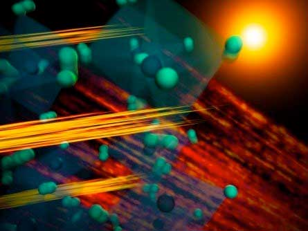
his illustration depicts what happens inside a hybrid perovskite material in the first few trillionths of a second after it's hit with simulated sunlight
This illustration depicts what happens inside a hybrid perovskite material in the first few trillionths of a second after it’s hit with simulated sunlight (upper left). The blue and green spheres are atoms, arranged in double pyramids as shown at left. When light hits, electrons start to separate from positively charged “holes,” the first step in creating an electrical current (yellow streaks). Meanwhile, atoms begin to vibrate within the perovskite’s lattice-like structure. Scientists detected these processes by analyzing the terahertz radiation (red streaks) the processes released. (Image: Greg Stewart/SLAC National Accelerator Laboratory)
The study is the first to probe the inner workings of hybrid perovskites at the atomic scale using laser pulses that match the intensity of solar radiation, and thus mimic natural sunlight. The authors say their discovery could lead to improvements in the performance of perovskite solar cells and a new way to probe their functionality.

Perovskites and Silicon

Most solar cells today are made of purified silicon manufactured at temperatures above 3,000 degrees Fahrenheit (1,600 degrees Celsius). These rigid silicon panels can last for decades in all kinds of weather conditions.
Perovskite solar cells, although far less durable, are thinner and more flexible than silicon cells and can be produced near room temperature from a hybrid mixture of cheap organic and inorganic materials, like iodine, lead and methylammonium.
Researchers, including Stanford co-author Michael McGehee, have shown that perovskite solar cells are as efficient at converting light to electricity as commercially available silicon cells and can even outperform them. This combination of efficiency, flexibility and easy synthesis has fueled a worldwide race to develop commercial-grade perovskites that can withstand long-term exposure to heat and precipitation.
“Perovskites are very promising materials for photovoltaics,” said lead author Burak Guzelturk, a postdoctoral scholar at Stanford and SLAC. “But people wonder how they can achieve such high efficiencies.”

Electrons and Holes

All solar cells operate on the same principle. Photons of sunlight absorbed by the crystalline material kick negatively charged electrons into an excited state. The freed electrons leave behind positively charged spaces or “holes” that separate from one another. This separation gives rise to an electric current.
Pure silicon, with its highly ordered atomic structure, provides a direct path for electrons and holes to travel through the solar cell. But with perovskites, the road is far from smooth.
“Perovskites are typically filled with defects,” said co-author Aaron Lindenberg, an associate professor at SLAC and Stanford and investigator with the Stanford Institute of Materials and Energy Sciences (SIMES). “They’re not even close to being perfect crystals, yet somehow the electric currents don’t see the defects.”

Terahertz Emission

For the study, the research team used laser pulses to simulate waves of sunlight from both ends of the visible light spectrum – high-energy violet light and low-energy infrared light. The results were measured at the picosecond timescale. One picosecond is one trillionth of a second.
“In the first picoseconds after sunlight hits the perovskite, the electrons and holes in the crystalline lattice start to split,” Lindenberg explained. “The separation was uncovered by measuring the emission of high-frequency terahertz light pulses oscillating a trillion times per second from the perovskite thin film. This is the first time anyone has observed terahertz emission from hybrid perovskites.”
The terahertz emission also revealed that electrons and holes closely interact with lattice vibrations in the crystalline material. This interaction, which occurs on a femtosecond timescale, could help explain how electric currents navigate through the patchwork of crystal grains in hybrid perovskites.
„As the electric charges separate, we observe a sharp spike in the terahertz emission, matching a vibrational mode of the material,” Guzelturk said. “That gives us clear evidence that the electrons and holes are strongly coupling with the atomic vibrations in the material.”
This finding raises the possibility that coupling to the lattice vibration could protect the electrons and holes from charged defects in the perovskite, shielding the electric current as it travels through the solar cell. Similar scenarios have been proposed by other research teams.
“This is one of the first observations of how the local atomic structure of a hybrid perovskite material responds in the first trillionths of a second after absorbing sunlight,” Lindenberg said. “Our technique could open up a new way of probing a solar cell right when the photon is absorbed, which is really important if you want to understand and build better materials. The conventional way is to put electrodes on the device and measure the current, but that essentially blurs out all of the microscopic processes that are key. Our all-optical, electrode-less approach with femtosecond time resolution avoids that problem.”

Hot Electrons

The researchers also found that terahertz light fields are much stronger when perovskite is hit with high-energy light waves.
“We found that radiated terahertz light is orders of magnitudes more intense when you excite the electrons with violet light versus low-energy infrared light,” Lindenberg said. “That was an unexpected result.”
This discovery could provide new insights on high-energy “hot” electrons, Guzelturk said.
“Violet light imparts electrons with excess kinetic energy, creating hot electrons that move much faster than other electrons,” he said. “However, these hot electrons lose their excess energy very rapidly.”
Harnessing the energy from hot electrons could lead to a new generation of high-efficiency solar cells, added Lindenberg.
“One of the grand challenges is finding a way to capture the excess energy from a hot electron before it relaxes,” he said. “The idea is that if you could extract the current associated with hot electrons before the energy dissipates, you could increase the efficiency of the solar cell. People have argued that it’s possible to create hot electrons in perovskites that live much longer than they do in silicon. That’s part of the excitement around perovskites.”
The study revealed that in hybrid perovskites, hot electrons separate from holes faster and more efficiently than electrons excited by infrared light.
“For the first time we can measure how fast this separation occurs,” Lindenberg said. “This will provide important new information on how to design solar cells that use hot electrons.”

Toxicity and Stability

The ability to measure terahertz emissions could also lead to new research on non-toxic alternatives to conventional lead-based perovskites, said Guzelturk.
“Most of the alternative materials being considered are not as efficient at generating electricity as lead,” he said. “Our findings might allow us to understand why lead composition works so well while other materials don’t, and to investigate the degradation of these devices by looking directly at the atomic structure and how it changes.”
Source: SLAC National Accelerator Laboratory

Un nou tip de biți cuantic în două dimensiuni(A new kind of quantum bits in two dimensions)

Două materiale noi, fiecare compus dintr-un singur strat atomic și vârful unui microscop de scanare – acestea sunt ingredientele pentru a crea un nou tip de așa numitul „punct cuantic”. Aceste nanostructuri extrem de mici permit controlul delicat al electronilor individuali prin reglarea fină a nivelului lor de energie direct. Astfel de dispozitive sunt esențiale pentru tehnologiile cuantice moderne.

Posted: Mar 19, 2018

A new kind of quantum bits in two dimensions

(Nanowerk News) Two novel materials, each composed of a single atomic layer and the tip of a scanning tunneling microscope – these are the ingredients to create a novel kind of a so-called „quantum dot”. These extremely small nanostructures allow delicate control of individual electrons by fine-tuning their energy levels directly. Such devices are key for modern quantum technologies.

The theoretical simulations for the new technology were performed in the team of Prof. Florian Libisch and Prof. Joachim Burgdörfer at TU Wien. The experiment involved the group of Prof. Markus Morgenstern at RWTH Aachen and the team around Nobel-prize laureates Andre Geim and Kostya Novoselov from Manchester who prepared the samples. The results have now been published in Nature Nanotechnology („Large tunable valley splitting in edge-free graphene quantum dots on boron nitride”).
text
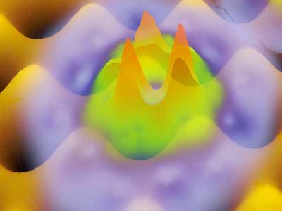
New kinds of quantum bits: Tiny nanostructures allow delicate control of individual electrons. (Image: TU Vienna)

Tuning electron energies

„For many applications in the field of quantum technologies one requires a quantum system were electrons occupy two states – similar to a classical switch – on or off, with the difference that quantum physics also allows for arbitrary superpositions of the on and off states” explains Florian Libisch from the Institute for Theoretical Physics at TU Wien.
A key property of such systems is the energy difference between those two quantum states: „Efficiently manipulating the information stored in the quantum state of the electrons requires perfect control of the system parameters. An ideal system allows for continuous tuning the energy difference from zero to a large value” says Libisch.
For systems found in nature – for example atoms – this is usually difficult to realize. The energies of atomic states, and hence their differences, are fixed. Tuning energies becomes possible in synthetic nanostructures engineered towards confining electrons. Such structures are often referred to as quantum dots or „artificial atoms”.

Two ultra-thin materials: graphene and hexagonal boron nitride

The international research team of TU Wien, RWTH Aachen and the University of Manchester now succeeded in developing a new type of quantum dots which allow for much more accurately and widely tunable energy levels of confined electrons than before. This progress was made possible by combining two very special materials: graphene, a conductive single atomic layer of carbon atoms, and hexagonal boron nitride, also a single layer of material quite similar to graphene except that it is insulating.
Exactly like graphene boron nitride also forms a honeycomb lattice. „The honeycombs in graphene and hexagonal boron nitride are, however, not exactly of equal size” explains Florian Libisch. „If you carefully put a single layer of graphene on top of hexagonal boron nitride, the layers cannot perfectly match. This slight mismatch creates a superstructure over distances of several nanometers, which results in an extremely regular wave-like spatial oscillation of the graphene layer out of the perfect plane.”
As the extensive simulations at TU Wien show, exactly these oscillations in graphene on hexagonal boron nitride form the ideal scaffold to control electron energies. The potential landscape created by the regular superstructure allows for accurately placing the quantum dot, or even moving it continuously and thus smoothly changing its properties. Depending on the exact position of the tip of the scanning tunneling microscope, the energy levels of the electronic states inside the quantum dot change. „A shift by a few nanometers allows for changing the energy difference of two neighboring energy levels from minus five to plus ten millielectronvolts with high accuracy – a tuning range about fifty times larger than previously possible”, explains Florian Libisch.

Towards „Valleytronics”

As a next step, the tip of the scanning tunneling microscope could be replaced by a series of nanoelectronic gates. This would allow for exploiting the quantum dot states of graphene on hexagonal boron nitride for scalable quantum technologies such as „valleytronics”.
„This emerging new field is quickly becoming a center of attention”, comments Florian Libisch. „There are multiple potential technological applications of these atomically thin materials – that is also why the TU Wien has also very recently established a special doctoral college focused on two-dimensional materials.”
Source: Vienna University of Technology

Ultra-alb nanocoating modelate pe scale scaun(Ultra-white nanocoating modelled on beetle scales)

Materialul – de 20 de ori mai alb decât hârtia – este fabricat din celuloză netoxică și atinge o alunecare atât de strălucitoare, imitând structura cântarelor ultra-subțiri ale anumitor tipuri de gândaci.Ca și cântarele de gândac, membranele de celuloză sunt extrem de subțiri: doar câteva milimi de un metru gros, deși cercetătorii spun că membranele chiar mai subțiri ar putea fi produse prin optimizarea în continuare a procesului lor de fabricare. Membranele împrăștie lumina de 20 până la 30 de ori mai eficient decât hârtia și ar putea fi utilizate pentru a produce materiale de lumină durabile și biologice compatibile de generație viitoare de ultimă generație.

Posted: Mar 15, 2018

Ultra-white nanocoating modelled on beetle scales

(Nanowerk News) The material – which is 20 times whiter than paper – is made from non-toxic cellulose and achieves such bright whiteness by mimicking the structure of the ultra-thin scales of certain types of beetle. The results are reported in the journal Advanced Materials („Anomalous-Diffusion-Assisted Brightness in White Cellulose Nanofibril Membranes”).

Bright colours are usually produced using pigments, which absorb certain wavelengths of light and reflect others, which our eyes then perceive as colour.
To appear as white, however, all wavelengths of light need to be reflected with the same efficiency. Most commercially-available white products – such as sun creams, cosmetics and paints – incorporate highly refractive particles (usually titanium dioxide or zinc oxide) to reflect light efficiently. These materials, while considered safe, are not fully sustainable or biocompatible.
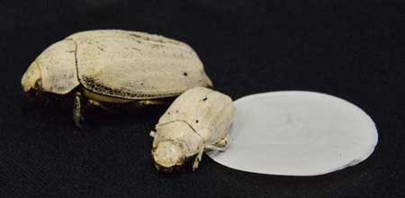
Cyphochilus beetle with cellulose-based coating
Cyphochilus beetle with cellulose-based coating. (Image: Olimpia Onelli)
In nature, the Cyphochilus beetle, which is native to Southeast Asia, produces its ultra-white colouring not through pigments, but by exploiting the geometry of a dense network of chitin – a molecule which is also found in the shells of molluscs, the exoskeletons of insects and the cell walls of fungi. Chitin has a structure which scatters light extremely efficiently – resulting in ultra-white coatings which are very thin and light.
“White is a very special type of structural colour,” said paper co-author Olimpia Onelli, from Cambridge’s Department of Chemistry. “Other types of structural colour – for example butterfly wings or opals – have a specific pattern in their structure which results in vibrant colour, but to produce white, the structure needs to be as random as possible.”
The Cambridge team, working with researchers from Aalto University in Finland, mimicked the structure of chitin using cellulose, which is non-toxic, abundant, strong and bio-compatible. Using tiny strands of cellulose, or cellulose nanofibrils, they were able to achieve the same ultra-white effect in a flexible membrane.
By using a combination of nanofibrils of varying diameters, the researchers were able to tune the opacity, and therefore the whiteness, of the end material. The membranes made from the thinnest fibres were more transparent, while adding medium and thick fibres resulted in a more opaque membrane. In this way, the researchers were able to fine-tune the geometry of the nanofibrils so that they reflected the most light.
“These cellulose-based materials have a structure that’s almost like spaghetti, which is how they are able to scatter light so well,” said senior author Dr Silvia Vignolini, also from Cambridge’s Department of Chemistry. “We need to get the mix just right: we don’t want it to be too uniform, and we don’t want it to collapse.”
Like the beetle scales, the cellulose membranes are extremely thin: just a few millionths of a metre thick, although the researchers say that even thinner membranes could be produced by further optimising their fabrication process. The membranes scatter light 20 to 30 times more efficiently than paper and could be used to produce next-generation efficient bright sustainable and biocompatible white materials.
Source: University of Cambridge

Noul lichid de centrifugare cuantic previzionat de Premiul Nobel pentru prima data(New quantum spin liquid predicted by Nobel Laureate prepared for the first time)

Supraconductoarele de temperatură ridicată sunt oxizi de cupru în care ionii de cupru formează o latură pătrată, astfel încât momentele magnetice adiacente se confruntă în direcții opuse. Când această structură este deranjată de modificarea stării de oxidare a cuprului, materialul devine supraconductor. În noile cercetări publicate acum, interacțiunile magnetice ale acestei structuri pătrate au fost modificate cu ioni cu o structură electronică d10 și d0, care a transformat materialul într-un lichid cu spin quantum

Posted: Mar 15, 2018

New quantum spin liquid predicted by Nobel Laureate prepared for the first time

(Nanowerk News) In 1987 Paul W. Anderson, a Nobel Prize winner in Physics, proposed that high-temperature superconductivity, or loss of electrical resistance, is related to an exotic quantum state now known as quantum spin liquid. Magnetic materials are made up of very tiny magnets, which can be as small as individual electrons. The strength and direction of these are described by the magnetic moment.

In quantum spin liquids, magnetic moments behave like a liquid and do not freeze or order even at absolute zero. These quantum states are being studied as promising materials for new, so-called topological quantum computers, in which operations are based on particle-like excited states found in quantum spin liquids.
In addition to large computational power, a topological quantum computer is characterised by high fault tolerance, which makes it possible to increase the size of the computer.
However, only a few quantum spin liquids suitable for topological quantum computers have been identified so far.
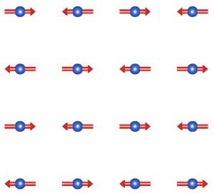
magnetically ordered square lattice of copper ions
The magnetically ordered square lattice of copper ions. Tailoring the structure caused the formation of quantum spin liquid. Modifying the structure in a different way results in high-temperature superconductivity. (Image: Otto Mustonen)

A method of tailoring the magnetism of materials developed at Aalto enabled the preparation of a new quantum spin liquid

Now, for the first time ever, researchers from Aalto University, Brazilian Center for Research in Physics (CBPF), Technical University of Braunschweig and Nagoya University have produced the superconductor-like quantum spin liquid predicted by Anderson.
This is an important step towards understanding superconductors and quantum materials. The preparation of a quantum spin liquid was made possible by a new way of tailoring the properties of magnetic materials that was developed by chemists at Aalto University. The results of the research have been published in Nature Communications („Spin-liquid-like state in a spin-1/2 square-lattice antiferromagnet perovskite induced by d10–d0 cation mixing”).
High-temperature superconductors are copper oxides in which the copper ions form a square lattice so that the adjacent magnetic moments face in opposite directions. When this structure is disturbed by changing the oxidation state of copper, the material becomes superconducting. In the new research now published, the magnetic interactions of this square structure were modified with ions with a d10 and d0 electronic structure, which turned the material into a quantum spin liquid.
“In the future, this new d10/d0 method can be utilised in many other magnetic materials, including various quantum materials”, envisions Doctoral Candidate Otto Mustonen from Aalto University.

Seamless cooperation

Empirical detection of quantum spin liquids is difficult and requires extensive research infrastructure.
muon spin spectrometer
The muon spin spectrometer used in the study at the Paul Scherrer Institute. The sample being studied is placed in the cryostat located in the middle, and a muon beam is aimed at it from the back left direction. (Image: Otto Mustonen)
“We used muon spin spectroscopy in the this study. This method is based on the interaction of very short-lived, electron-like elementary particles, known as muons, with the material being studied. The method can detect very weak magnetic fields in quantum materials”, says Professor F. Jochen Litterst from the Technical University of Braunschweig. The measurements were performed at the Paul Scherrer Institute in Switzerland.
“In addition to top-class equipment, the research requires seamless cooperation between chemists and physicists”, emphasises Professor Maarit Karppinen. “We’re going to need the same international multidisciplinary approach in the future so that this research on quantum spin liquids can lead us to the experimental realization of the topological quantum computer.”
Source: Aalto University

Graphene găsește o nouă aplicație ca colorant anti-static non-toxic(Graphene finds new application as non-toxic, anti-static hair dye)

Oamenii ar putea aplica acest colorant pentru a face părul conductiv la suprafață”, a spus Huang. „Acesta ar putea fi apoi integrat cu electronice portabile sau să devină o sondă conductivă. Suntem limitați doar de imaginația noastră „Echipa a utilizat grafenul super-material pentru a dezvolta un nou colorant pentru păr, care este non-toxic, nu dăunează și durează prin multe spălări fără să se estompeze. Grafenul conduce, de asemenea, natura deschiderii de noi oportunități pentru păr, cum ar fi transformarea acestuia în electrozi in situ sau integrarea acestuia cu dispozitive electronice portabile.

Posted: Mar 15, 2018

Graphene finds new application as non-toxic, anti-static hair dye

(Nanowerk News) It’s an issue that has plagued the beauty industry for more than a century: Dying hair too often can irreparably damage your silky strands.

Now a Northwestern University team has used materials science to solve this age-old problem. The team has leveraged super material graphene to develop a new hair dye that is non-toxic, non-damaging and lasts through many washes without fading. Graphene’s conductive nature also opens up new opportunities for hair, such as turning it into in situ electrodes or integrating it with wearable electronic devices.
The study was published by the journal Chem („Multifunctional Graphene Hair Dye”). Jiaxing Huang, professor of materials science and engineering in Northwestern’s McCormick School of Engineering, led the research.
Dying hair might seem simple and ordinary, but it’s actually a sophisticated chemical process. Called the cuticle, the outermost layer of a hair is made of cells that overlap in a scale-like pattern. Commercial dyes work by using harsh chemicals, such as ammonia and bleach, to first pry open the cuticle scales to allow colorant molecules inside and then trigger a reaction inside the hair to produce more color. Not only does this process cause hair to become more fragile, some of the small molecules are also quite toxic.
Huang and his team bypassed harmful chemicals altogether by leveraging the natural geometry of graphene sheets. While current hair dyes use a cocktail of small molecules that work by chemically altering the hair, graphene sheets are soft and flexible, so they wrap around each hair for an even coat. Huang’s formula also incorporates edible, non-toxic polymer binders to ensure that the graphene sticks – and lasts through at least 30 washes, which is the commercial requirement for permanent hair dye. An added bonus: graphene is anti-static, so it keeps winter-weather flyaways to a minimum.
“It’s similar to the difference between a wet paper towel and a tennis ball,” Huang explained, comparing the geometry of graphene to that of other black pigment particles, such as carbon black or iron oxide, which can only be used in temporary hair dyes. “The paper towel is going to wrap and stick much better. The ball-like particles are much more easily removed with shampoo.”
This geometry also contributes to why graphene is a safer alternative. Whereas small molecules can easily be inhaled or pass through the skin barrier, graphene is too big to enter the body. “Compared to those small molecules used in current hair dyes, graphene flakes are humongous,” said Huang, who is a member of Northwestern’s International Institute of Nanotechnology.
Ever since graphene – the two-dimensional network of carbon atoms – burst onto the science scene in 2004, the possibilities for the promising material have seemed nearly endless. With its ultra-strong and lightweight structure, graphene has potential for many applications in high-performance electronics, high-strength materials and energy devices. But development of those applications often require graphene materials to be as structurally perfect as possible in order to achieve extraordinary electrical, mechanical or thermal properties.
The most important graphene property for Huang’s hair dye, however, is simply its color: black. So Huang’s team used graphene oxide, an imperfect version of graphene that is a cheaper, more available oxidized derivative.
“Our hair dye solves a real-world problem without relying on very high-quality graphene, which is not easy to make,” Huang said. “I feel optimistic about this application.”
Still, future versions of the dye could someday potentially leverage graphene’s notable properties, including its highly conductive nature.
“People could apply this dye to make hair conductive on the surface,” Huang said. “It could then be integrated with wearable electronics or become a conductive probe. We are only limited by our imagination.”
So far, Huang has developed graphene-based hair dyes in multiple shades of brown and black. Next, he plans to experiment with more colors.
Source: By Amanda Morris, Northwestern University

Graphene oxide nanopheets ar putea ajuta aduce litiu-metal baterii la piață(Graphene oxide nanosheets could help bring lithium-metal batteries to market)

sub forma unei nanoplocuri acoperite cu oxid de grafena care, atunci cand sunt plasate intre cei doi electrozi ai unei baterii metal-litiu, previne placarea neuniforma a litiului și permite funcționarea în siguranță a bateriei pentru sute de cicluri de încărcare / descărcare;Arătăm că materialele bidimensionale de oxid de grafen sunt capabile să împiedice formarea dendritelor prin schimbarea vitezei de difuzie a litiu-ionului pe măsură ce trec prin straturile de oxid de grafen

Posted: Mar 15, 2018

Graphene oxide nanosheets could help bring lithium-metal batteries to market

(Nanowerk News) Lithium-metal batteries – which can hold up to 10 times more charge than the lithium-ion batteries that currently power our phones, laptops and cars – haven’t been commercialized because of a fatal flaw: as these batteries charge and discharge, lithium is deposited unevenly on the electrodes. This buildup cuts the lives of these batteries too short to make them viable, and more importantly, can cause the batteries to short-circuit and catch fire.

Now, researchers at the University of Illinois at Chicago have developed a solution to this problem in the form of a graphene-oxide coated ‘nanosheet’ that, when placed in between the two electrodes of a lithium-metal battery, prevents uneven plating of lithium and allows the battery to safely function for hundreds of charge/discharge cycles. They report their findings in the journal Advanced Functional Materials („Synergistic Effect of Graphene Oxide for Impeding the Dendritic Plating of Li”).
lithium electrode in a battery with a graphene oxide nanosheet separator
Left: Dendrites forming on a lithium electrode. Right: Lithium plates uniformly on a lithium electrode in a battery with a graphene oxide nanosheet separator. (Image: Reza Shahbazian-Yassar) (click on image to enlarge)
„Our findings demonstrate that two-dimensional materials – in this case, graphene oxide – can help regulate lithium deposition in such a way that extends the life of lithium-metal batteries,” said Reza Shahbazian-Yassar, associate professor of mechanical and industrial engineering in the UIC College of Engineering and corresponding author of the paper.
Lithium-metal batteries are so useful because of their high-energy density and relatively light weights compared with conventional batteries. However, over the course of many charge-discharge cycles, lithium builds up unevenly on the battery’s lithium metal electrode in a branching or ‘dendritic’ pattern and ultimately causes the battery to go dead. If the dendrites grow through the electrolyte solution and make contact with the other electrode, then the battery may experience a catastrophic event – in other words, an explosion or fire.
In lithium-ion batteries, a separator is placed in the electrolyte. Usually made of a porous polymer or glass ceramic fibers, the separator allows lithium ions to flow through while keeping the other components blocked to prevent electrical shorts, which can lead to fires.
Reza and colleagues used a modified separator in a lithium-metal battery to modulate the flow of lithium ions to control the rate of lithium deposition and see if they could prevent dendrites from forming. They spray-coated a fiberglass separator with graphene oxide, producing what they called a nanosheet.
Using scanning electron microscopy and other imaging techniques, the researchers showed that when the nanosheet was used in a lithium-metal battery, a uniform film of lithium formed on the lithium electrode’s surface, which actually improves battery function and makes the battery much safer, said Tara Foroozan, a graduate student in the UIC College of Engineering and first author on this study.
Molecular simulations, led by a team of researchers from Texas A & M University, suggested that the lithium ions become temporarily bonded to the graphene oxide, and then diffuse through areas of nanoscopic defects in the sheet. This delays the passage of lithium ions enough to prevent the formation of dendritic deposition of lithium on the electrode.
„The nanosheet slows the passage of lithium ions enough to allow for more uniform plating on lithium ions across the surface of the electrode, which helps preserve battery life,” said Reza.
Results of phase-field modeling computations led by Farzad Mashayek, professor and head of mechanical and industrial engineering in the UIC College of Engineering and an author on the paper, indicated that graphene oxide can also mechanically suppress the growth of lithium dendrites.
„We show that two-dimensional graphene oxide materials are able to impede the formation of dendrites by changing the rate of lithium-ion diffusion as they pass through the graphene oxide layers,” said Shahbazian-Yassar. „This method has very high potential for industrial application and scalability.”
Source: University of Illinois at Chicago

Filtrul de apă pe bază de grafen elimină mai mult de 99% din materia organică naturală(Graphene-based water filter removes more than 99% of natural organic matter)

au dezvoltat un filtru de laborator pe scara larga, bazat pe grafen, care poate elimina mai mult de 99% din materia organica omniprezenta naturala ramasa in urma tratarii conventionale a apei potabile.Noul sistem de tratare se face prin transformarea grafitului natural in membranele de oxid de grafena care permit un debit mare de apa la presiunea atmosferica, in timp ce se elimina practic toata materia organica

Posted: Mar 14, 2018

Graphene-based water filter removes more than 99% of natural organic matter

(Nanowerk News) University of New South Wales (UNSW) scientists have developed a world-first, graphene-based, laboratory-scale filter that can remove more than 99% of the ubiquitous natural organic matter left behind during conventional treatment of drinking water.

In a research collaboration with Sydney Water, the team has demonstrated the success of the approach in laboratory tests on filtered water from the Nepean Water Filtration Plant in western Sydney, and is working to scale up the new technology.
The results of some of the ground-breaking research are published in the journal Carbon(„Application of graphene oxide membranes for removal of natural organic matter from water”). The project is led by Dr Rakesh Joshi of the UNSW School of Materials Science and Engineering, in collaboration with Professor Veena Sahajwalla and Professor Vicki Chen of UNSW, and Dr Heriberto Bustamante of Sydney Water.
“Our advance is to use filters based on graphene – an extremely thin form of carbon. No other filtration method has come close to removing 99% of natural organic matter from water at low pressure,” Dr Joshi said.
“Our results indicate that graphene-based membranes could be converted into an alternative new option that could in the future be retrofitted in conventional water treatment plants.”
Sydney Water supplies clean water to about 4.8 million people in Sydney, the Illawarra and the Blue Mountains. These natural organic matter contaminants can affect the performance of direct filtration plants, reducing their capacity after heavy rain.
“The most common methods used at present to remove organic matter from water supplies include the application of chemical coagulants,” said Dr Bustamante.
“However, these existing treatments are only partly effective, particularly as the concentration of natural organic matter is increasing.”
Dr Joshi said: “The new treatment system is made by converting naturally occurring graphite into graphene oxide membranes that allow high water flow at atmospheric pressure, while removing virtually all of the organic matter.”
Dr Joshi has an international reputation in this area, having published many highly cited articles including one in the journal Science on graphene oxide-based filtration in 2014 while working at the University of Manchester with Nobel Laureate Sir Andre Geim.
The UNSW team is upgrading the experimental rig to construct a small pilot plant that could be tested in the field.
Source: By Deborah Smith, University of New South Wales

Scoaterea metalelor grele din apă cu MOF(Removing heavy metals from water with MOFs)

cadre organice metalice (MOF), materiale care sunt realizate din noduri metalice interconectate cu substanțe chimice organice ” struts’. Suprafața lor internă fără precedent și o ușurință chimică ușoară permite MF să „tragă” vaporii de apă și alte gaze din aer. Aceleași caracteristici le fac materiale promițătoare, de asemenea, pentru eliminarea selectivă a metalelor grele din apă ( ACS Central Science , „Rapidă, selectivă de eliminare a metalelor grele din apă printr-un cadru metalo-organic / polidopamină compozit” ).Compozitul final, denumit Fe-BTC / PDA, poate elimina rapid și selectiv cantități mari de metale grele cum ar fi plumbul și mercurul din probele de apă din lumea reală. De fapt, el poate elimina de peste 1,6 ori greutatea proprie a mercurului și de 0,4 ori greutatea sa de plumb.

Posted: Mar 14, 2018

Removing heavy metals from water with MOFs

(Nanowerk News) According to the World Health Organization almost 1 billion people do not have access to clean drinking water, and that number is expected to increase with climate change. Meanwhile, our endlessly rising energy needs and use of heavy metals in industrial processes have maximized our exposure to toxic materials in water.

Current commercial methods to remove heavy metals including lead from municipal drinking water tend to be costly and energy-consuming, without being sufficiently efficient. Less conventional approaches might be more efficient, but are single-use, difficult to regenerate, or produce significant toxic waste as a side-product.
Now, the lab of Professor Wendy Lee Queen at EPFL, with colleagues at the University of California Berkeley and Lawrence Berkeley National Laboratory have found a solution using metal organic frameworks (MOFs), which are materials made up of metal nodes interlinked by organic chemical ‘struts’. Their unprecedented internal surface areas and easy chemical tunability allow MOFs to „pull” water vapor and other gases from air. These same features make them promising materials also for selectively removing heavy metals from water (ACS Central Science, „Rapid, Selective Heavy Metal Removal from Water by a Metal–Organic Framework/Polydopamine Composite”).
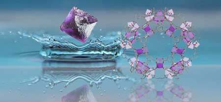
A drop of water injected on an octahedral crystal
A drop of water injected on an octahedral crystal. (Image: Wendy Lee Queen/EPFL)
A PhD student at EPFL-Valais, Daniel T. Sun, has designed a water-stable MOF/polymer composite using cheap, environmentally and biologically friendly materials. The scientists treated a MOF, known as Fe-BTC, with dopamine, which polymerized to polydopamine (PDA) pinning the polymer inside the MOF. The final composite, named Fe-BTC/PDA, can quickly and selectively remove high amounts of heavy metals like lead and mercury from real-world water samples. In fact, it can remove over 1.6 times its own weight of mercury and 0.4 times of its weight of lead.
Fe-BTC/PDA was then tested in solutions as toxic as some of the worst water samples found in Flint, Michigan. The tests showed that the MOF can, in a matter of seconds, reduce lead concentrations to 2 parts per billion, a level that the U.S. Environmental Protection Agency and World Health Organization deem drinkable.
The scientists also removed lead from various real-world water samples obtained from the Rhone River, the Mediterranean Sea, and a wastewater treatment plant in Switzerland. They also showed how the material could be regenerated easily.
There are multiple sources of exposure to toxic heavy metals. For example, lead is used in paint, ceramic glazes, jewelry, toys, and pipes. Considering this, the approach with the new MOF shows much promise for solving current limitations of water-cleaning systems. The authors of the study are now testing other new specially designed MOFs to remove other types of trace contaminants in water and air.
Source: Ecole Polytechnique Fédérale de Lausanne