Noul ceramică nanostructurată transformă căldura risipită în electricitate

a proiectat ceramică nanostructurată, care sunt materiale termoelectrice care convertesc căldura produsă în procesele industriale în energie electrică.
Pentru a găsi o sursă alternativă de energie, cercetătorul modelează și proiectează aceste materiale pentru a fi utilizate în diferite industrii, cum ar fi spațiul sau automobilul, pentru a reutiliza căldura eliberată în conducta de eșapament a unei mașini.

Posted: Mar 01, 2016

Novel nanostructured ceramics convert wasted heat into electricity

(Nanowerk News) Talia Alvarez, currently studying her doctorate at the University Of Manchester, UK, designed nanostructured ceramics, which are thermoelectric materials that convert the heat produced un industrial processes into electrical energy.

In order to find an alternative energy source, the researcher shapes and designs these materials for use in different industries, such as space or automobile, in the latter to reuse the heat released in the exhaust pipe of a car.
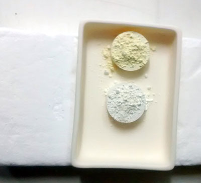
Nanostructured ceramics
Nanostructured ceramics.
The air temperature exiting said device is at approximately 800 degrees kelvin, and causes the exhaust pipe of an automobile to reach between 700 and 600 degrees Celsius. A temperature difference that can be used to generate electricity, said Alvarez Ruiz, master of science in electrical engineering from the Center of Research and Advances Studies (CINVESTAV) in Mexico.
The aim is to create a ceramic with excellent chemical conditions, which is economical and coats the tube leakage or engine of a vehicle. This assures the recovery of heat and savings on fuel.
More than two thirds of the energy released in burning fossil fuel is wasted as heat and released to the environment. Besides the machines, vehicles, even the human body produces this energy source that goes to waste, said Alvarez Ruiz.
In search for cheap ceramics
The native of Tapachula, Chiapas, in the south of Mexico, shapes and designs nanostructured ceramics which main component is zinc oxide, a semiconductor used in industry, abundant in nature, economical and environmentally friendly.
„What I do is play with the chemical composition of the material and the manufacturing process to improve the properties, because the current ceramics with high efficiency are expensive and toxic”.
Alvarez Ruiz seeks a ceramic that does not have these toxic characteristics. The problem is that the temperature difference needs to be very large and so far in the laboratory only a small voltage is obtained.
„Commercial materials have an efficiency of 4, mine has an efficiency of 0.6. The difference is large but the advantages are many, we aim to reduce production costs that in the future will be beneficial to society.”
Ceramics designed at the University of Manchester could be implemented to take advantage of the heat released in thermoelectric plants and generate enough electricity to power light bulbs.
Source: Investigación y Desarrollo

Read more: Novel nanostructured ceramics convert wasted heat into electricity

Fizicienii primesc un material perfect pentru filtrele de aer

demonstrat că reducerea diametrului fibrelor de la 200 nanometri până la 20 a redus rezistența filtrului la fluxul de aer cu două treimi și acest efect nu mai poate fi explicat prin aerodinamica clasică. Când dimensiunea obstacolului este mai mică decât calea liberă a moleculelor de gaze, metodele standard care estimează rezistența aerodinamică bazată pe teoria continuumului nu mai funcționează. În condiții normale, calea medie liberă a moleculelor de aer produce 65 nanometri.

Posted: Mar 01, 2016

Physicists get a perfect material for air filters

(Nanowerk News) A research team from the Institute of Theoretical and Experimental Biophysics of the Russian Academy of Sciences have synthesized the material that is perfect for protection of respiratory organs, analytical research and other practical purposes. An almost weightless fabric made of nylon nanofibers with a diameter less than 15 nm beats any other similar materials in terms of filtering and optical properties.

The scientists whose work is published in Macromolecular Nanotechnology Journal („Filtering and optical properties of free standing electrospun nanomats from nylon-4,6”), characterize their material as lightweight (10-20 mg/m2), almost invisible (95% light transmission: more than that of a window glass), showing low resistance to airflow and efficient interception of <1 micrometer fine particulate matter.
An almost weightless fabric made of nylon nanofibers with a diameter less than 15 nm
A sample of the new fabric in reflected light. (Image courtesy of the researchers)
The wording „nanofibers” in the researchers’ article is more than a fashion statement. Previously, the same team demonstrated that reducing fiber diameter from 200 nanometers down to 20 decreased filter resistance to airflow by two thirds, and this effect could no longer be explained by classical aerodynamics. When an obstacle size is smaller than the free path of gas molecules, the standard methods estimating aerodynamic resistance based on the continuum theory no longer work. In normal conditions, the mean free path of air molecules makes 65 nanometers.
The mean free path is the average distance one molecule manages to cover before colliding with another. Only if all obstacles are much bigger than this value, the free stream coming at them can be rightfully considered a continuous medium.
The scientists used the technique called electrospinning: a jet of a dissolved polymer is ejected through a special nozzle aiming at a target under action of an electric field. From the other side, ethanol is electrosprayed. The polymer jet and the alcohol ions take the opposite electric charges. Colliding in the air, they form ultra-thin fibrous films. Electrospinning technology as a way to produce nonwoven fibrous filters has been developed back in the 50s to purify air in atomic industry. However, the researchers introduced an important improvement: instead of obtaining nanomats on a solid conducting substrate like before, now with the new technology, a free filter is formed covering a 55-mm hole in a non-conductive polycarbonate screen.
The published work completed the cycle of the authors’ papers devoted to development of the manufacturing technology and studies of properties of nanofilters manufactured using this new process. It was established that the unique optical and filtering properties originate from a special mechanism of „healing” holes and defects in free standing filters. Such holes literally attract fibers landing onto the filter surface. As a result, a good filter without big holes can be obtained from a minimum amount of nanofibers and, accordingly, with a minimum resistance to airflow. Moreover, active healing of big holes between threads provides the filters with the properties inherent in filters with calibrated pores, so called track-etched membranes (Nuclepores). The scientists have also demonstrated that the „healing” mechanism does not work in the conventional electrospinning technique where nanofibers are deposited onto a conducting substrate completely at random.
The testing of nylon-4,6 electrospun films showed that thess almost weightless and invisible fabrics trap no less than 98% of airborne dust particles. For testing, the scientists used particles from 0.2 to 0.3 micron in diameter. This roughly corresponds to the dust that is not caught by the nasal pharynx, and penetrates the lungs causing a number of dangerous medical conditions. Submicron particles (< 1 micrometer in diameter) are the ones also used to test industrial and medical filters. To assess performance, resistance to airflow is tested as well.
Experiments to measure resistance have been made on singular samples so far. In real filters a multi-layer surface with a complex configuration is normally used. The experiments showed that the nylon-4,6 filtering material had the best properties out of all types of fabric previously described . In terms of interception extent to filter weight ratio and interception-resistance to airflow ratio, the new filtering material beats any existing equivalents by several times.
At first it looks like a ring sitting on a sheet of paper. In reality, it is a sample of the new fabric for filters. The small red spot on top of „l” letter is a spot wherea laser beam penetrates the film. Low intensity of dispersed light demonstrates high transparency of the new material. A transmission index of the new product is higher than that of a good window glass. The picture is courtesy of the researchers.
Speaking about possible applications of this material, the scientists claim it is more than the obvious air and water purification from particulate matter. Since the material surpasses glass in transparency, it can be used in biological research. For example, after pumping air or water through the new filter intercepted microorganisms may be directly observed right on the transparent filter under a microscope. Again, this effect is due to ultra-fine threads. Their thickness is significantly less than even visible light wavelength.
Source: Moscow Institute of Physics and Technology

Read more: Physicists get a perfect material for air filters

Testarea nedistructivă: Privind în interiorul compozitelor

Cercetarea utilizează compozite cu legături de înaltă calitate și altele în mod deliberat făcute cu legături mai slabe. Diferențele în rezultatele de a ajuta echipa îmbunătăți detectarea defectelor sau deteriorare. Un ecran de computer prezinta pete luminoase sau întunecate indică posibilele probleme care, și a realiza un grafic legăturile suprapuși adâncimea probleme potențiale la timpul indicat pe imagine.

Posted: Feb 01, 2016

Nondestructive testing: Looking inside composites

(Nanowerk News) Researcher David Moore holds a rectangle of hard carbon composite material, smooth with a faint woven pattern on its surface. The sample shows normal wear and tear until he turns it over to reveal a circular impact mark with cracks radiating from it.

The question for Moore, his Sandia National Laboratories colleague Timothy Briggs in California and their teams is whether the impact caused significant, hidden damage inside the composite. They’re developing nondestructive ways to detect damage in composites, using traditional medical inspection techniques such as X-rays and sonograms and advanced methods including infrared imaging, ultrasonic spectroscopy and computed tomography.
Sandia National Laboratories technologist Andrew Lentfer passes a roller probe over a composite as researcher David Moore checks data on a screen
Sandia National Laboratories technologist Andrew Lentfer passes a roller probe over a composite as researcher David Moore checks data on a screen. The nondestructive testing technique sends sound waves into the composite material, returning data with each swipe of the roller probe.
Sandia began studying composites several years ago to see whether the lightweight materials could be used in national security applications. While a composite in a cell phone needs to last only a couple of years, “typically materials for national security applications must survive for decades. This makes you think differently about where and why you would use a material,” said Moore, who works in the Structural Dynamics and X-ray/Nondestructive Evaluation department. “We need to study the lifecycle of a component. We tend to think deeply about the consequences of fracture or deformation and how we can verify what happened.”
The work supports many aspects of Sandia’s national security mission, including energy efficiency and performance improvements in lightweight vehicles or wind turbine blades, said Briggs of Sandia California’s Lightweight Structures organization.
Composites join together separate materials with different characteristics. They often consist of a soft polymer matrix with reinforcing fibers like carbon, Kevlar or glass. Composites can use bundles of thinner-than-a-hair carbon strands that yield a high strength-to-weight ratio. The final shape and strength is obtained after heating the part in an industrial oven that sets the polymer resin and yields the qualities necessary for a structural component.
Composites are increasingly important in aerospace and other industries because they’re strong and weigh less than metals. Most can be bonded to metal for such uses as aircraft wings, making planes lighter and less expensive to fly.
Outside surface of a composite doesn’t hint at what’s inside
“We have a rich history of understanding metals and their failure mechanisms,” Moore said. “Composite materials are very different.”
If a service truck backs into a composite aircraft fuselage, an examination of the impact site might not detect damage under the surface. That highlights the reason for nondestructive techniques that can fully evaluate how composites react in various circumstances.
The research team is assessing the accuracy of nondestructive methods and how they could be used on a production floor. “You have to know what could go wrong in the processing steps and how to circumvent those, and then you want to make sure if you’re going to make one or a hundred or a thousand that you’re making them the same way all the time,” Moore said.
“Once we establish the limits of detectability, the threshold of good, bad and questionable, we’ll be able to say, ‘We want this composite bonded to this material with a defined quality and it shall be inspected with this technique,’” he said.
Sandia’s Lightweight Structures Lab defines and consolidates materials to study, using particular stack sequences of composite material layers to tailor strength and stiffness. It works in concert with the National Security Campus in Kansas City, Missouri, in everything from developing process methods to building prototypes to qualifying designs for particular applications.
After making composites, the fabrication lab cuts out specimens for instrumented experiments — abusing the carefully made sample to study deformation, fracture and damage growth. Briggs “pulls, stretches, torques and crushes them. He performs these mechanical experiments so we can understand the fracture mechanisms around failure,” Moore said. “Then we try to detect some of those failure modes.”
Characterizing material properties helps computer modeling, simulation
“The fundamental characterization of composites measures material properties and structural characteristics, which in turn provides information to validate computer modeling and simulation,” Briggs said.
Data from these destructive tests is correlated with nondestructive evaluations from Moore’s team to understand what caused the material to respond the way it did, Briggs said. The effort hinges on close collaboration with Sandia’s materials characterization groups and modeling and simulation colleagues to help validate their computer-based simulations.
Composites must support a particular weight and size. “Anyone can build a structure to carry the load, but we have to design our structures to fit within a geometric envelope and be lightweight,” Briggs said. “We cannot simply over-engineer to unrealistic levels. We have to be very smart and efficient with our designs, yet provide enough margin for long-term reliability.”
Materials bonded in an oven or autoclave often have different thermal expansion rates — aluminum expands more than fiber-reinforced plastics, for example. Once a composite cools after curing, residual stresses can build up inside, particularly at interfaces. If the composite can’t handle those stresses, the bonds can fail.
Sandia is developing advanced techniques to complete sample inspections in less than 5 minutes in some cases. “This is a way to gain a lot of information very quickly about the quality of the bonds,” Moore said.
Team studies specific nondestructive techniques
His team uses the deliberately mistreated composites to assess such inspection techniques as advanced ultrasonics, flashed or active thermography and computed tomography.
Ultrasonic testing has been around for 60 years, but computers and other improvements now allow study of more complex applications. Technologist Andrew Lentfer demonstrates, scanning a piece of composite with a handheld ultrasonic roller that resembles a small paint roller with a hollow, water-filled barrel. As he scans the composite’s layers, a computer screen maps them in color: Yellow-green is OK; blue indicates weakness. Rollers can scan curved surfaces, even large ones like airplanes.
Fibers and interfaces in a composite scatter ultrasonic waves moving through the material. Moore compares it to ocean waves: “If a wave hits a rock face in the ocean it moves around it; if a wave washes up on the sand it gets absorbed; and if it hits a seawall the wave energy is redirected quickly. Those are the same fundamentals we investigate: ultrasonic energy moving through a composite matrix.”
Knowledge gained from characterizing materials helps develop new nondestructive techniques “so when we establish an inspection criteria, we have a better feel for what we can detect and what we cannot,” he said.
Flashed thermography, commercially available for more than 20 years, flashes very high-energy light onto a surface for 15 microseconds, then an infrared camera watches how the surface cools. The process takes only minutes.
“It’s very fast, but you have to understand the fundamentals of heat flow and how the material surface either gives off heat to its surroundings or transfers heat within itself,” Moore said.
Studies use good, not-so-good composites to test differences
The research uses composites with high-quality bonds and others deliberately made with weaker bonds. Differences in results help the team improve detection of defects or damage. A computer screen shows light or dark spots indicating possible problems, and an overlaid graph ties the depth of the potential problem to the time indicated on the image.
“The question becomes, is that a concern? Is that a crack or not?” Moore said. “We’ll be able to answer those questions. If the defect propagates deep into the material, we may not detect it. It’s wise to understand the capabilities of the technique and then perform the math and science behind it.”
Computed tomography systems are efficient for finding small defects. The technique rotates a sample 360 degrees while taking 1,000 images, similar to a medical CT scan, and generates an image from each thin slice of the object. Since each image taken is two dimensional, computer algorithms reconstruct, calculate, locate and display everything to represent the object in three dimensions.
“Once the 3-D image is reconstructed, you look at the front surface and then start moving through the thickness to view what is below the surface,” Moore said. “This technology gives us a knowledge baseline and validates how the other techniques are performing.”
Sandia must ensure designs meet requirements by specifying and qualifying an inspection technique, and now is writing inspection procedures for the National Security Campus, Moore said. “Once we establish criteria and limits of acceptability, the product definition can be established,” he said.
Source: Sandia National Laboratories

Read more: Nondestructive testing: Looking inside composites

Nanotehnologia în textile – noul negru

Acoperirea suprafeței textile și îmbrăcăminte cu nanoparticule este o abordare a producției de suprafețe extrem de active pentru a avea UV-blocare, antimicrobiene, antistatic retardant, flacără, apă și ulei hidrofug, rezistent la rid, și auto-curățare properties.One obstacol încăpățânat făcut previne textile îmbunătățită nanomaterial de a deveni mai mult o realitate comercială este insuficientă durabilitatea acoperirilor nano pe fibre textile sau stabilitatea diferitelor proprietăți înzestrate de nanoparticule. Pur și simplu pune, „inteligent“ vine de pe timpul proprietăților antimicrobiene washing.While sunt exercitate de nano-argint, blocarea UV, auto-curățare și proprietăți ignifuge sunt conferite de acoperiri de oxid de nano-metal. nanoparticule de oxid de zinc încorporate în matrici polimerice, cum ar fi amidon solubil sunt un exemplu bun de nanostructuri funcționale cu potențial de aplicații, cum ar fi: capacitatea de protectie UV in industria textila si de protectie solara si finisaje antibacteriene in textile medicale si interioara Wears

Posted: Feb 29, 2016

Nanotechnology in textiles – the new black

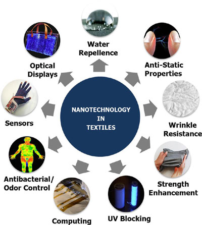
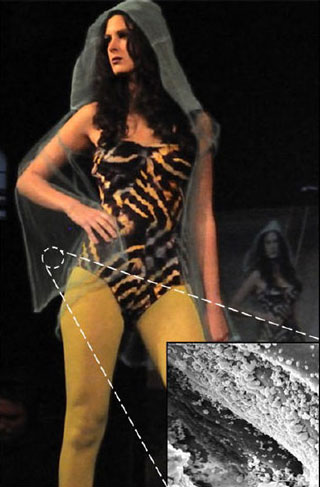
(Nanowerk Spotlight) Nanoengineered functional textiles are going to revolutionize the clothing that you’ll wear. The potential of nanotechnology in the development of new materials in the textile industry is considerable. On the one hand, existing functionality can be improved using nanotechnology and on the other, it could make possible the manufacture of textiles with entirely new properties or the combination of different functions in one textile material (read our previous Nanowerk Spotlight on this topic: „Nanotechnology textiles„).Applications of nanotechnology in textilesApplications of nanotechnology in textiles. (Reprinted with permission by American Chemical Society)A first generation of nano-enhanced textiles benefitted from nano finishing: Coating the surface of textiles and clothing with nanoparticles is an approach to the production of highly active surfaces to have UV-blocking, antimicrobial, antistatic, flame retardant, water and oil repellent, wrinkle resistant, and self-cleaning properties.One stubborn hurdle that prevents nanomaterial-enhanced textiles from becoming more of a commercial reality is the insufficient durability of nanocoatings on textile fibers or the stability of various properties endowed by nanoparticles. Quite simply put, the ‘smart’ comes off during washing.While antimicrobial properties are exerted by nano-silver, UV blocking, self-cleaning and flame-retardant properties are imparted by nano-metal oxide coatings. Zinc oxide nanoparticles embedded in polymer matrices like soluble starch are a good example of functional nanostructures with potential for applications such as UV-protection ability in textiles and sunscreens, and antibacterial finishes in medical textiles and inner wears (read more about nanofinishing in textile technology).Permethrin-releasing textile net on a body suitSandy Mattei models a design by Matilda Ceesay with a Permethrin-releasing textile net. (Image: Cornell University)A just published review paper in the February 26, 2016 online edition of ACS Nano („Nanotechnology in Textiles”) discusses electronic and photonic nanotechnologies that are integrated with textiles and shows their applications in displays, sensing, and drug release within the context of performance, durability, and connectivity.In these smart clothes the textile structures themselves perform electronic or electric functions. Ideally, the nanoelectronic components will be completely fused with the textile material, resulting in that textile and non-textile components cannot be differentiated and ‘foreign particles’ can no longer be seen or felt.
Electronics in textiles

We have written extensively about smart textiles, for instance

In their review, the authors discuss the electrical conductivity of conducting polymers and graphene, both of which are attractive for creating textiles that enable the incorporation of sensors and actuators.Another section of the review is dedicated to power sources suitable for e-textiles. This covers lightweight fabric carbon nanotube supercapacitor electrodes; stretchable graphene and PPy-based supercapacitors; triboelectric nanogenerators; flexible fiber and stripe batteries; and stretchable PPy-based supercapacitors for energy transfer.Schematic illustration of a wearable triboelectric nanogenerator(a) Schematic illustration of a wearable triboelectric nanogenerator. (b) Fabrication process of the nanopatterned PDMS structure. (c) FE-SEM images of the bottom textile with nanopatterned PDMS. Inset is a high-resolution image clearly showing the ZnO NR-templated PDMS nanopatterns. (d) Photographic image of the flexible, foldable WTNG. (Reproduced with permission by American Chemical Society) (click on image to enlarge)Adding digital components to these e-textiles would open up an entirely new area of functional clothing. OLEDs in fiber form could lead to revolutionary applications by integrating optical and optoelectronic devices into textile. Combined with nanoelectronic devices, we might one day see flexible optical sensors and display screens woven into shirts and other garments. You could literally wear your next-generation smart phone or iPad on your sleeves; including the solar panels to power them (read more: „Light-emitting nanofibers shine the way for optoelectronic textiles„).


Photonic technologies for textiles

Want your clothes to change color at the push of a button, in response to ambient heat or illumination, warning you about airborne pollutants or pollen, or glow in the dark? The integration of optical technologies into garments will make this possible.As the authors write, „photonic materials and devices including films, nanoadditives, or optical fibers have been adopted in the fabrication of textiles and garments to not only enhance the aesthetic performance but also endow the garments with additional functionalities. The most distinctive and basic application of optical technologies on fabrics or garments is perhaps tuning their appearance by controlling the intensity, color, and pattern of light.”For example, optical films made of periodical dielectric multilayers could be directly coated on fabrics, thus offering a highly reflective colorful appearance and enabling different color perceptions depending on the angle of observation. Holographic films may also achieve similar functions and even provide a more complex 3D visual effect.”

Sensing and drug release in textiles

Lab-on-fiber technology will allow the implementation of sophisticated, autonomous multifunction sensing and actuating systems – all integrated in individual optical fibers. Such multifunctional labs integrated into a single optical fiber, exchanging information and combining sensorial data, could provide effective auto-diagnostic features as well as new photonic and electro-optic functionalities (read more: „Move over chips – here come multifunctional labs on a single fiber„).The general sensing principle of a plasmonic fiber sensor is described in detail in the review paper: „In a plasmonic fiber sensor, a lossy surface plasmon mode propagating along a metal/dielectric interface can be excited at its resonance by an optical fiber core-guided mode via evanescent wave coupling when the phase-matching condition between the two modes is satisfied at a certain frequency. The presence of such a plasmonic mode manifests itself as a spectral dip in the fiber transmission spectrum, with its spectral location corresponding to the phase-matching frequency. Variations in the refractive index of an analyte adjacent to the metal layer could significantly modify the phase-matching condition, thus displacing the spectral dip in the optical fiber transmission spectrum.”Already, temperature, humidity, and pressure sensors have been incorporated in textiles. In future, microfluidics can be incorporated in thread-based channels for application in point-of-care diagnostics. Combined with LEDs, these textiles can give visual sensing information. Combined with drug-loaded nanoparticles, textile fibers could provide programmable release of therapeutic drugs.For example, the designer Matilda Ceesay created a hooded body suit embedded at the molecular level with insecticides to ward off mosquitoes infected with malaria. The cotton mesh used for this anti-malaria garment was coated with a material where an insect repellent and fabric are bound at the nano level using metal organic framework molecules (MOFs).Concluding their review, after an extensive discussion of fabrication methods and functionalities, the authors also address the issues of toxicity of nanomaterials in textiles as well as commercial trends in the global nanotechnology-enhanced textile market.By Michael is author of two books by the Royal Society of Chemistry: Nano-Society: Pushing the Boundaries of Technology and Nanotechnology: The Future is Tiny.

Read more: Nanotechnology in textiles – the new black

Nanotehnologia în textile – noul negru(Nanotechnology in textiles -the new black)

potențialul nanotehnologiei în dezvoltarea de noi materiale în industria textilă este considerabil;autorii abordează, de asemenea, problemele legate de toxicitatea nanomaterialelor din textile, precum și tendințele comerciale în domeniul nanotehnologiei globale – îmbunătățirea pieței textile

s37

Controlerul piezo-digital de înaltă performanță PI de înaltă performanță este prea eficient din punct de vedere al costurilor

Specificații, foaie de date, mai multe informații
Aplicațiile E-727
Aplicațiile includ nanopoziția, nano-automatizarea, tehnologia semiconductorilor, fotonica, bio-nanotehnologia, metrologia, microscopia, micro-manipularea, inclusiv aplicațiile curate.
Caracteristici și avantaje
– Servo Digital pentru algoritmi avansați de control
– Lățime de bandă de control de 25 kHz
– Pentru senzori de feedback cu capacitate și piezo-rezistență
– Intrări și ieșiri de control analogic de înaltă rezoluție
– Interfețe: Ethernet, USB și RS-232
– Intrări și ieșiri digitale
– DSP 32/64-bit, Floating Point, 375 MHz
– DAC pe 20 biți și rezoluție ADC
– ID Chip compatibil pentru interschimbabilitatea controlerului și a mecanicii
– Linia 4 din ordinul polinomial


Posted: Feb 29, 2016

PI’s New High Performance Multi-Channel Digital Piezo Controller is Cost-Effective Too

(Nanowerk News) PI (Physik Instrumente) L.P., an industry leader in precision motion components, systems, and solutions, has released a new, high-performance 3 and 4-channel digital piezo controller that integrates with a wide range of existing piezo-based nanpositioning systems and piezo actuators.
E-727 controller
Lower Price, Higher Performance
The new E-727 replaces the E-725 controller and combines higher performance with a lower price. Compared to its predecessor, it provides 3 additional high-resolution analog interfaces, a faster servo, as well as a broader choice of traditional, high-speed, and real time digital interfaces, such as SPI, Ethernet, USB and RS-232
Ultra-Low Noise Controller
20-bit DAC & ADC converters keep the closed-loop E-727 controller operating with high resolution and ultra-low noise, along with 4 integrated power amplifiers for multilayer piezo drives with operating voltage of -30 to +130V. Closed-loop nanopositioning systems are supported with capacitive feedback sensors, piezoresistive sensors, and traditional strain gauges. In addition to PID control, 2 additional user programmable notch filters are implemented for suppression of mechanical system resonances. Linearization based on 4th order polynomials provides higher positioning accuracy. The Dynamic Digital Linearization (DDL) feature eliminates non-linearities at high operating frequencies.
Data Recorder, Auto-Calibration ID Chip, Quick Start UP, Comprehensive Software Package The cost-effective E-727 has a data recorder for high speed tracing, ID chip compatibility for quick start-up, and exchange of system components without recalibration, and the additional feature of programmable drift compensation. The controller comes with extensive software support for LabVIEW and shared libraries for Windows and Linux. Multiple digital interfaces for ease of control: Ethernet, USB, RS-232, SPI. Four (4) digital I/O channels as well as four (4) high-resolution analog inputs and outputs each are also available for use with external sensors, target values or external amplifiers.
Specifications, Datasheet, More Information
Applications of the E-727
Applications include nanopositioning, nano-automation, semiconductor technology, photonics, bio-nano-technology, metrology, microscopy, micro-manipulation, including cleanroom applications.
Features & Advantages
  • – Digital Servo for Advanced Control Algorithms
  • – 25 kHz Control Bandwidth
  • – For Capacitive and Piezo-restive Strain Gauge Feedback Sensors
  • – High Resolution Analog Control Inputs and Outputs
  • – Interfaces: Ethernet, USB, and RS-232
  • – Digital Inputs and Outputs
  • – DSP 32/64-bit Floating Point, 375 MHz
  • – 20-bit DAC and ADC Resolution
  • – ID Chip Compatible for Interchangeability of Controller and Mechanics
  • – 4th Order Polynomial Linearization for Mechanics & Electronics
About PI
PI is a leading manufacturer of precision motion control equipment, piezo motors, air bearing stages and hexapod parallel-kinematics for semiconductor applications, photonics, bio-nano-technology and medical engineering. PI has been developing and manufacturing standard & custom precision products with piezoceramic and electromagnetic drives for 4 decades. The company has been ISO 9001 certified since 1994 and provides innovative, high-quality solutions for OEM and research. PI is present worldwide with eleven subsidiaries, R&D / engineering on 3 continents and total staff of 800+.
Source: PI (press release)

Read more: PI’s New High Performance Multi-Channel Digital Piezo Controller is Cost-Effective Too

Scrutând(cercetand) vârful sondelor moleculare

Autorii au folosit date din spectroscopie infraroșie și termogravimetrie pentru a identifica rezistența interacțiunii dintre sondă și suprafața de oxid, care le-a ajutat, de asemenea, să determine tipul de legare la suprafață.
Ei au stabilit doi parametri cheie: în primul rând, densitatea speciilor de suprafață adsorbite utilizate pentru a caracteriza interacțiunea moleculei de sondă cu suprafața. Acest parametru depinde de natura nanoparticulelor de oxid și de existența nanoporilor. Al doilea parametru exprimă raportul dintre moleculele conținute în stratul de suprafață având un comportament dinamic din sticlă față de numărul total al moleculelor adsorbite.
Studiul arată că valoarea densității de suprafață poate fi utilizată pentru a diviza compozitele în mai multe grupuri. Acest lucru ajută la determinarea faptului că moleculele de sondă aplicate pe suprafața unui grup dat pot prezenta interacțiuni similare, așa cum se observă în suprafețele aceleiași familii.

Posted: Feb 29, 2016

Scrutinizing the tip of molecular probes

(Nanowerk News) Studies of molecules confined to nano- or micropores are of considerable interest to physicists. That’s because they can manipulate or stabilise molecules in unstable states or obtain new materials with special properties.

In a new study published in EPJ Plus („Rod-like cyanophenyl probe molecules nanoconfined to oxide particles: Density of adsorbed surface species”), Stefan Frunza from the National Institute of Materials Physics in Romania and colleagues have discovered the properties of the surface layer in probe molecules on the surface of oxide particles. These properties depend on the interaction at the interface.
In this particular study, probes are formed by adsorption of rod-like cyanophenyl derivates on the surface of oxide particles. The authors found that their surface layers behave like glass-forming liquids.
The solid lines indicate the temperature range used to estimate the amount of molecules loaded onto the probe
The solid lines indicate the temperature range used to estimate the amount of molecules loaded onto the probe.
What physicists already knew is that confinement of molecules may induce disorder. Confinement and disorder have a considerable influence both on the structure of the trapped molecule but also on its mobility. As a result, they also affect aspects such as molecular dynamics upon relaxation of the material. Such structurally well-defined monolayers on solid surfaces will allow researchers to model a large variety of interfacial phenomena.
The authors used data from infrared spectroscopy and thermogravimetry to identify the strength of the interaction between the probe and the oxide surface, which also helped them determine the type of bonding to the surface.
They established two key parameters: firstly, the density of the adsorbed surface species used to characterise the interaction of the probe molecule with the surface. This parameter depends on the nature of the oxide nanoparticles and on the existence of nanopores. The second parameter expresses the ratio of the molecules contained in the surface layer having a glassy dynamic behaviour to the total number of the adsorbed molecules.
The study shows that the value of the surface density can be used to divide the composites into several groups. This helps to determine that the probe molecules applied to the surface of a given group can display similar interactions, as observed in surfaces of the same family.
Source: SciencePOD

Read more: Scrutinizing the tip of molecular probes

Forma nouă a imaginilor cu fascicul de electroni poate vedea elemente care sunt „invizibile” pentru metodele comune

Această placă de fază modifică fasciculul de electroni într-un mod care permite modificarea subtilă a unui material care poate fi măsurat, chiar dezvăluind materiale care ar putea fi invizibile în imaginile STEM tradiționale.
O altă metodă bazată pe electroni, pe care cercetătorii o utilizează pentru a determina structura detaliată a probelor biologice delicate și congelate, se numește microscopie crioelectronică sau crio-EM. În timp ce cryo-EM cu particule unice este un instrument puternic – a fost numit ca revista științifică Nature’s 2015 Method of the Year – este de obicei nevoie de a lua o medie peste multe eșantioane identice pentru a fi eficiente. În general, Cryo-EM nu este util pentru studierea probelor cu un amestec de elemente grele (de exemplu, majoritatea tipurilor de metale) și elemente ușoare cum ar fi oxigenul și carbonul.
Metoda MIDI-STEM ofera speranta pentru a vedea structuri cu un amestec de elemente grele si luminoase, chiar si atunci cand acestea sunt adunate in stransa legatura

Posted: Feb 29, 2016

New form of electron-beam imaging can see elements that are ‘invisible’ to common methods

(Nanowerk News) Electrons can extend our view of microscopic objects well beyond what’s possible with visible light – all the way to the atomic scale. A popular method in electron microscopy for looking at tough, resilient materials in atomic detail is called STEM, or scanning transmission electron microscopy, but the highly-focused beam of electrons used in STEM can also easily destroy delicate samples.

This is why using electrons to image biological or other organic compounds, such as chemical mixes that include lithium – a light metal that is a popular element in next-generation battery research – requires a very low electron dose.
Scientists at the Department of Energy’sc Lawrence Berkeley National Laboratory (Berkeley Lab) have developed a new imaging technique, tested on samples of nanoscale gold and carbon, that greatly improves images of light elements using fewer electrons.
MIDI-STEM Setup
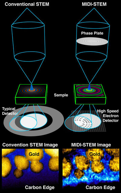
In MIDI-STEM (right), developed at Berkeley Lab, an electron beam travels through a ringed „phase plate,” producing a high-resolution image (bottom right) that provides details about a sample containing a heavy element (gold) and light element (carbon). Details about the carbon are missing in an image (bottom left) of the sample using a conventional electron imaging technique (ADF-STEM). (Image: Colin Ophus/Berkeley Lab)
The newly demonstrated technique, dubbed MIDI-STEM, for matched illumination and detector interferometry STEM, combines STEM with an optical device called a phase plate that modifies the alternating peak-to-trough, wave-like properties (called the phase) of the electron beam.
This phase plate modifies the electron beam in a way that allows subtle changes in a material to be measured, even revealing materials that would be invisible in traditional STEM imaging.
Another electron-based method, which researchers use to determine the detailed structure of delicate, frozen biological samples, is called cryo-electron microscopy, or cryo-EM. While single-particle cryo-EM is a powerful tool–it was named as science journal Nature’s 2015 Method of the Year –it typically requires taking an average over many identical samples to be effective. Cryo-EM is generally not useful for studying samples with a mixture of heavy elements (for example, most types of metals) and light elements like oxygen and carbon.
„The MIDI-STEM method provides hope for seeing structures with a mixture of heavy and light elements, even when they are bunched closely together,” said Colin Ophus, a project scientist at Berkeley Lab’s Molecular Foundry and lead author of a study, published Feb. 29 in Nature Communications („Efficient linear phase contrast in scanning transmission electron microscopy with matched illumination and detector interferometry”), that details this method.
If you take a heavy-element nanoparticle and add molecules to give it a specific function, conventional techniques don’t provide an easy, clear way to see the areas where the nanoparticle and added molecules meet.
„How are they aligned? How are they oriented?” Ophus asked. „There are so many questions about these systems, and because there wasn’t a way to see them, we couldn’t directly answer them.”
While traditional STEM is effective for „hard” samples that can stand up to intense electron beams, and cryo-EM can image biological samples, „We can do both at once” with the MIDI-STEM technique, said Peter Ercius, a Berkeley Lab staff scientist at the Molecular Foundry and co-author of the study.
The phase plate in the MIDI-STEM technique allows a direct measure of the phase of electrons that are weakly scattered as they interact with light elements in the sample. These measurements are then used to construct so-called phase-contrast images of the elements. Without this phase information, the high-resolution images of these elements would not be possible.
In this study, the researchers combined phase plate technology with one of the world’s highest resolution STEMs, at Berkeley Lab’s Molecular Foundry, and a high-speed electron detector.
They produced images of samples of crystalline gold nanoparticles, which measured several nanometers across, and the super-thin film of amorphous carbon that the particles sat on. They also performed computer simulations that validated what they saw in the experiment.
The phase plate technology was developed as part of a Berkeley Lab Laboratory Directed Research and Development grant in collaboration with Ben McMorran at University of Oregon.
The MIDI-STEM technique could prove particularly useful for directly viewing nanoscale objects with a mixture of heavy and light materials, such as some battery and energy-harvesting materials, that are otherwise difficult to view together at atomic resolution.
It also might be useful in revealing new details about important two-dimensional proteins, called S-layer proteins, that could serve as foundations for engineered nanostructures but are challenging to study in atomic detail using other techniques.
In the future, a faster, more sensitive electron detector could allow researchers to study even more delicate samples at improved resolution by exposing them to fewer electrons per image.
„If you can lower the electron dose you can tilt beam-sensitive samples into many orientations and reconstruct the sample in 3-D, like a medical CT scan. There are also data issues that need to be addressed,” Ercius said, as faster detectors will generate huge amounts of data. Another goal is to make the technique more „plug-and-play,” so it is broadly accessible to other scientists.
Source: Lawrence Berkeley National Laboratory

Read more: New form of electron-beam imaging can see elements that are ‘invisible’ to common methods

Nanoparticule pe nanosteps

au dezvoltat un material care menține stabilitatea A unui catalizator „dispersat^ și de constând dintr-un singur atom și de modalitatea de a produce boabe mici de platină prin exploatarea proprietăților substratului
Platina este unul dintre metalele costisitoare utilizate ca catalizatori în noile tehnologii folosite pentru procesele chimice industriale, sursele de energie regenerabilă, controlul poluării și multe alte scopuri. În special, se utilizează pentru celulele de combustie, dispozitive care transformă energia chimică direct în energie electrică, fără ardere. Cercetările au arătat că cea mai mare eficiență este obținută atunci când catalizatorul este disponibil sub formă de nanoparticule (mai mici de 10-9 m). Pur și simplu, cu cât este mai mare dispersia materialului și cu cât dimensiunea particulelor este mai mică, cu atât mai mult este disponibilă pentru cataliză. Din nefericire, legile termodinamicii determină particulele să se „lipsească” unul de celălalt și să formeze clustere mai mari, motiv pentru care materialul devine mai puțin eficient în timp. Deci, ce se poate face pentru a menține dispersia maximă a „nanopulberii”

Posted: Feb 29, 2016

Nanoparticles on nanosteps

(Nanowerk News) New technologies are starved for efficient and inexpensive catalysts. The best materials are made up of nanoparticles, whose properties are the result of their small size. The single catalyst particles have, however, an ugly tendency to cluster into larger particles, thereby reducing their effectiveness. A group of scientists from the International School of Advanced Studies in Trieste and the DEMOCRITOS centre of the Istituto Officina dei Materiali of the Italian National Research Council (IOM-CNR), with the collaboration of other institutions, have developed a material that maintains the stability of a “dispersed” catalyst, thus maximising the efficiency of the process and decreasing costs and wastage.

The study has just been published in Nature Communications („Creating single-atom Pt-ceria catalysts by surface step decoration”).
 Nanoparticles
Nanoparticles adhering to steps.
Platinum is one of the costly metals used as catalysts in new technologies employed for industrial chemical processes, renewable energy sources, pollution control and many other purposes. In particular, it is used for fuel cells, devices that turn chemical energy directly into electrical energy, without combustion. Research has shown that the greatest efficiency is achieved when the catalyst is available in the form of nanoparticles (smaller than 10-9 m). Simply put, the greater the dispersion of the material and the smaller the size of the particles, the more is it available for catalysis. Unfortunately, the laws of thermodynamics cause the particles to “stick” to one another and form larger clusters, which is why the material becomes less effective over time. So what can be done to maintain maximal dispersion of the “nanopowder”?
A group of SISSA/CNR IOM scientists (with the collaboration of the Univerzita Karlova in Prague) has studied a way to produce tiny platinum grains consisting of one atom only and to keep them dispersed in a stable manner, by exploiting the properties of the substrate on which they rest.
“Theoretical work demonstrated that irregularities in the surface known as steps and observed in experiments conducted at the Trieste Synchrotron tend to attract and separate the nanoparticles, causing them to remain literally attached in the form of single atoms”, explains Stefano Fabris, CNR-IOM/SISSA research fellow.
“The particles adhering to the steps were no longer visible even using an atomic resolution microscope” explains Nguyen-Dung Tran, a SISSA PhD student. “However, their presence was detected by spectroscopy, so they were indeed there, but they were no longer visible or free to move around”. “Our computer simulations solved this dilemma, showing that the particles on the steps are reduced to single atoms” adds Matteo Farnesi Camellone (CNR-IOM), another author of the study.
“If the surface is engineered to contain a large number of these defects, then the force that binds the particles to the substrate effectively offsets the aggregation force”, explains Fabris. The theoretical work, led by Fabris, allowed the researchers to develop a “system model” on the computer able predict the behaviour of the material. The model’s predictions were confirmed by the experimental measurements. Materials like this can be used for fuel cell electrodes, with far lower costs than the current ones.
“Reducing the amount of platinum used in fuel cell electrodes is a priority, not only to contain costs but also to ensure environmental sustainability, as also indicated by the recent European directives” concludes Fabris. The European project ChipCAT, which funded this research, aims precisely to achieve this goal.
Source: SISSA

Read more: Nanoparticles on nanosteps

Dispozitive electronice extensibile, care au o lungime cvadruple

ar putea fi folosit pentru senzori concepuți pentru a monitoriza anumite funcții biologice.Ideale pentru pielea artificială pe proteze sau mașini robotizateÎnlătură termen: îmbrăcăminte conectată și senzori pe corp îmbrăcăminte conectată și senzori pe corp

Posted: Feb 29, 2016

Stretchable electronics that quadruple in length (w/video)

(Nanowerk News) EPFL researchers have developed conductive tracks that can be bent and stretched up to four times their original length. They could be used in artificial skin, connected clothing and on-body sensors.

stretchable electronics
Conductive tracks are usually hard printed on a board. But those recently developed at EPFL are altogether different: they are almost as flexible as rubber and can be stretched up to four times their original length and in all directions. And they can be stretched a million times without cracking or interrupting their conductivity. The invention is described in an article published today in the journal Advanced Materials („Intrinsically Stretchable Biphasic (Solid–Liquid) Thin Metal Films”).
Both solid and flexible, this new metallic and partially liquid film offers a wide range of possible applications. It could be used to make circuits that can be twisted and stretched – ideal for artificial skin on prosthetics or robotic machines. It could also be integrated into fabric and used in connected clothing. And because it follows the shape and movements of the human body, it could be used for sensors designed to monitor particular biological functions.
“We can come up with all sorts of uses, in forms that are complex, moving or that change over time,” said Hadrien Michaud, a PhD student at the Laboratory for Soft Bioelectronic Interfaces (LSBI) and one of the study authors.
Extensive research has gone into developing an elastic electronic circuit. It is a real challenge, as the components traditionally used to make circuits are rigid. Applying liquid metal to a thin film in polymer supports with elastic properties naturally seems like a promising approach.
Thin and reliable
Owing to the high surface tension of some of these liquid metals, experiments conducted so far have only produced relatively thick structures. “Using the deposition and structuring methods that we developed, it’s possible to make tracks that are very narrow – several hundredths of a nanometer thick – and very reliable,” said Stéphanie Lacour, holder of the Bertarelli Foundation Chair in Neuroprosthetic Technology and who runs the lab.
Apart from their unique fabrication technique, the researchers’ secret lies in the choice of ingredients, an alloy of gold and gallium.
“Not only does gallium possess good electrical properties, but it also has a low melting point, around 30o,” said Arthur Hirsch, a PhD student at LSBI and co-author of the study. “So it melts in your hand, and, thanks to the process known as supercooling, it remains liquid at room temperature, even lower.” The layer of gold ensures the gallium remains homogeneous, preventing it from separating into droplets when it comes into contact with the polymer, which would ruin its conductivity.
Source: By Sarah Perrin, École polytechnique fédérale de Lausanne (EPFL)

Read more: Stretchable electronics that quadruple in length (w/video)