Stivuirea pe grafen(Stacking on the graphene)

Cercetătorii din Japonia au găsit o modalitate de a forma două materiale, fiecare realizat din trei straturi de grafen. Ghepena fiecărui material este stivuită diferit și are proprietăți electrice unice. Munca lor are implicații pentru dezvoltarea unor noi dispozitive electronice, cum ar fi senzorii foto care convertesc lumina în energie electrică.

Posted: Feb 09, 2018

Stacking on the graphene

(Nanowerk News) Researchers in Japan have found a way to form two materials, each made of three layers of graphene. Each material’s graphene is stacked differently and has unique electrical properties. Their work has implications for the development of novel electronic devices, such as photo sensors that convert light into electrical energy.

In 2004, two scientists realized they had isolated a single layer of carbon atoms on a scotch tape used to clean a graphite crystal. Since then, graphene has captured the imagination of researchers due to its fascinating properties: it is 200 times stronger than steel, is very flexible, and it is an excellent conductor of electricity.
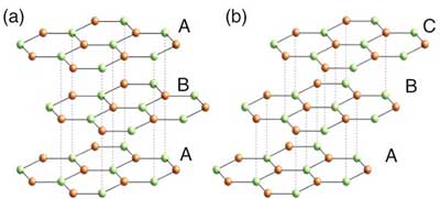
Graphene’s carbon atoms are arranged into hexagons, forming a honeycomb-like lattice. Placing one layer of graphene on top of another leads to the formation of bilayer graphene. The layers can be arranged in one of two positions: the centres of the carbon hexagons of each layer can be organized immediately above one another, called AA-stacking, or they can be displaced forwards so that a hexagon centre in one layer is above a carbon atom below it, called AB-stacking. AB-stacking of two layers of graphene leads to the formation of a material with semiconducting properties by applying an external electric field.
The schematic crystal structures of (a) ABA- and (b) ABC- stacked three layer graphene
The schematic crystal structures of (a) ABA- and (b) ABC- stacked three layer graphene. (Image: Katsuaki Sugawara)
Deliberately stacking three layers of graphene has proven difficult. But doing so could help researchers study how the physical properties of tri-layered materials change based on how the layers are stacked. This could lead to the development of novel electrical devices.
Researchers at Japan’s Tohoku University and Nagoya University have now fabricated two different types of trilayer graphene with different electrical properties.
They heated silicon carbide using one of two methods. In one experiment, silicon carbide was heated to 1,510°C under pressurized argon. In another, it was heated to 1,300°C in a high vacuum. Both materials were then sprayed with hydrogen gas in which the bonds were broken to form single hydrogen atoms. Two types of trilayer graphene then formed. The silicon carbide heated under pressurized argon formed into ABA-stacked graphene, in which the hexagons of the top and bottom layers were exactly aligned while the middle layer was slightly displaced. The silicon carbide heated in a vacuum developed into ABC-stacked graphene, in which each layer was slightly displaced in front of the one below it.
The researchers then examined the physical properties of each material and found that their electrons behaved differently.
The ABA graphene was an excellent electrical conductor, similar to monolayer grapheme. The ABC grapheme, on the other hand, acts more like AB graphene in that it had semi-conductor properties.
„The present success in selective fabrication of ABA and ABC trilayer graphene would widen the feasibility of graphene-based nano-electronic devices with variable layer numbers and stacking sequences,” conclude the researchers in their study published in the journal NPG Asia Materials(„Selective fabrication of free-standing ABA and ABC trilayer graphene with/without Dirac-cone energy bands”).
Source: Tohoku University

Metasuprafețele permit o performanță îmbunătățită a obiectivelor optice(Metasurfaces enable improved optical lens performance)

Obiectivele lentile apochromatice – cele care focalizează în mod corespunzător cele trei culori roșu, albastru și verde – care au o curbură mai mică și sunt mai subțiri și mai ușoare ar putea îmbunătăți camerele telefonului mobil și permit fabricarea de telefoane celulare mai subțiri. De asemenea, acestea ar putea face camere mai ușoare, mai bune pentru corp, camere pentru cască, zone de lunetist, dispozitive de imagistică termică și vehicule aeriene fără pilot sau dronuri. În esență, orice lucru care folosește lentile pentru imagine poate fi simplificat și mai ușor.

Posted: Feb 09, 2018

Metasurfaces enable improved optical lens performance

(Nanowerk News) Producing the perfect color images we need and love often requires multiple, heavy lenses so that each color focuses in exactly the same plane. Now Penn State engineers have developed a new theory that solves the problem using a single thin lens comprised of gradient index materials and metasurface layers to properly direct the light.

„If we want high performance optical systems, then we have to overcome material dispersion,” said Sawyer D. Campbell, assistant research professor in electrical engineering. „If we don’t, we get smeary colors, which significantly degrades image quality.”
Single apochromatic lenses – ones that properly focus the three colors red, blue and green – that have less curvature and are thinner and lighter could improve cell phone cameras and allow manufacture of thinner cell phones. They also could make lighter, better body cameras, helmet cameras, sniper scopes, thermal imaging devices and unmanned aerial vehicles or drones. In essence, anything that uses lenses to image could be made simpler and lighter.
„Usually there are several lenses, but that increases the weight,” said Jogender Nagar, graduate student in electrical engineering. „Our aim is to improve SWaP – reduce size and weight while increasing performance.”
The researchers thought to combine two technologies: that of gradient-index (GRIN) lens, and metasurfaces – ultra-thin optical layers with sub-wavelength features that manipulate the wavefront in a desired manner. The researchers report the results of their work in the current issue of Optica („Multi-element, multi-frequency lens transformations enabled by optical wavefront matching”).
focussing light through lenses
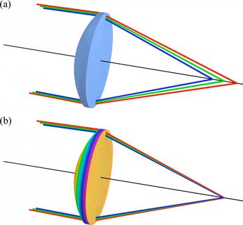
Traditional glass lenses (a) focus different colors to different points resulting in color separation and image blurring. In contrast, newly developed metasurface-augmented gradient-index lenses (b) correct for color separation by focusing blue, green, and red light to the same point. (Image: Jogender Nagar, Penn State)
„Our system uses one lens,” said Nagar. „We use the curvature of the lens, the distribution of materials in the lens, and a metasurface – a pattern placed on the surface – to make the lens thinner, lighter, but still focus properly.”
Most lenses use curvature to control the focal point, but three separate conventional lenses are needed to focus the three separate colors to one focal point and produce a high quality image. By spatially varying the material composition inside the lens, one GRIN lens can perfectly focus two colors. Then, by adding a metasurface to the GRIN lens, one layered lens can perfectly focus all three colors and do the work of three conventional lenses.
„The gradient in the lens can be axial – varying along the direction of light propagation, or optical axis; or radial – varying outwardly from the optical axis,” said Douglas H. Werner, John L. and Genevieve H. McCain Chair Professor in electrical engineering. „Or it could be more complex.”
The researchers developed a theoretical model and simulation framework for creating these lenses.
„We had to use some advanced tools that were specially developed in the lab,” said Werner. „Tools for modeling, simulation and optimization that we created for solving such a challenging design problem.”
The theoretical model specifies the proper surface curvature and gradient in the GRIN lens and the proper patterning for the metasurface to satisfy the requirements of perfect focusing of all three colors. The model optimizes both the lens and the metasurface to work together.
„The theory is very general and covers a wide range of conditions,” said Werner. „Fabrication will be the challenge initially. We hope development of the theory will steer the fabrication, making it possible to produce such lenses at a low cost and high volume.”
Source: Penn State

Filme adezive antimicrobiene inovatoare pentru reducerea riscului de infecție în spitale(Innovative antimicrobial adhesive films to reduce infection risk in hospitals)

Grupul de Cercetare al Universității din Alicante în analiza polimerilor și nanomaterialelor, împreună cu personalul din industrie și cercetare din Italia, … este implicat în proiectul FLEXPOL de a face un film adeziv antimicrobian care reduce riscul de infecție în spitale

Innovative

Printare, camuflaj colorat cu polimeri(Printable, colorful camouflage with polymers)

că au dezvoltat polimeri care pot imita mai bine abilitățile naturii de a schimba culoarea decât polimerii existenți. Se spune că materialele ar putea permite decorarea inteligentă, textilele de camuflaj și măsurile de combatere a contrafacerii îmbunătățite.

Posted: Feb 07, 2018

Printable, colorful camouflage with polymers

(Nanowerk News) In nature, colors can serve as a form of communication, but they can also hide animals and plants, camouflaging them from sight. Researchers now report in ACS Applied Materials & Interfaces („Full Color Camouflage in a Printable Photonic Blue-Colored Polymer”) that they have developed polymers that can better mimic nature’s color-changing abilities than existing polymers. They say the materials could enable smart decorations, camouflage textiles and improved anti-counterfeiting measures.

Printable, Colorful Camouflage with Polymers
Newly developed polymer can better mimic nature’s color-changing abilities. (Image: American Chemical Society)
Most of the colors that people are familiar with, such as hues on a piece of paper, are made with pigments. But another type, called structural color, exists, in which the color is produced by periodically arranged microscopic structures that interfere with visible light.
For example, peacock tail feathers are actually brown, but microscopic structures present in the feathers make them look blue and green to the naked eye. Scientists have used cholesteric liquid-crystalline (CLC) polymers to mimic the structural coloration found in nature because they can easily be made into responsive materials. But so far, researchers have only produced them in a limited range of colors. So Albertus P. H. J. Schenning and Monali Moirangthem wanted to make CLC polymers with the full visible spectrum of colors.
The team used inkjet printing technology and a calcium nitrate solution to print an image on a CLC polymer they developed. Printing successive layers changed the degree of swelling of the CLC polymer, changing the color. One layer resulted in an orange color, a second layer changed it to green, and a third layer made it blue.
As an example, the researchers used the method to draw a blue flower with green leaves on a reddish-orange background. After the ink dried, the image was no longer visible–the entire surface appeared blue. However, sprinkling water or breathing on it caused the full color image to re-appear.
Source: American Chemical Society

Super lemnul ar putea înlocui oțelul(Super wood could replace steel)

au gasit o modalitate de a face lemnul de peste 10 ori mai puternic si mai dur decat inainte, creand o substanta naturala mai puternica decat multe aliaje de titan.
„Acest nou mod de a trata lemnul îl face de 12 ori mai puternic decât lemnul natural și de 10 ori mai dur”.Acest lucru ar putea fi un concurent pentru oțel sau chiar aliaje de titan, este atât de puternic și durabil. Este de asemenea comparabil cu fibra de carbon, dar mult mai puțin costisitor”

Posted: Feb 07, 2018

Super wood could replace steel

(Nanowerk News) Engineers at the University of Maryland, College Park (UMD) have found a way to make wood more than 10 times times stronger and tougher than before, creating a natural substance that is stronger than many titanium alloys.

„This new way to treat wood makes it 12 times stronger than natural wood and 10 times tougher,” said Liangbing Hu of UMD’s A. James Clark School of Engineering and the leader of the team that did the research, to be published on February 8, 2018 in the journal Nature(„Processing bulk natural wood into a high-performance structural material”).
Liangbing Hu and Teng Li, University of Maryland
Liangbing Hu, left, and Teng Li, right, are engineers at the University of Maryland, College Park who have found a way to make wood more than 10 times stronger and tougher than before. (Image: University of Maryland)
„This could be a competitor to steel or even titanium alloys, it is so strong and durable. It’s also comparable to carbon fiber, but much less expensive.” Hu is an associate professor of materials science and engineering and a member of the Maryland Energy Innovation Institute.
„It is both strong and tough, which is a combination not usually found in nature,” said Teng Li, the co-leader of the team and Samuel P. Langley Associate Professor of mechanical engineering at UMD’s Clark School. His team measured the dense wood’s mechanical properties. „It is as strong as steel, but six times lighter. It takes 10 times more energy to fracture than natural wood. It can even be bent and molded at the beginning of the process.”
The team also tested the new wood material and natural wood by shooting bullet-like projectiles at it. The projectile blew straight through the natural wood. The fully treated wood stopped the projectile partway through.
„Soft woods like pine or balsa, which grow fast and are more environmentally friendly, could replace slower-growing but denser woods like teak in furniture or buildings,” Hu said.
„The paper provides a highly promising route to the design of lightweight, high performance structural materials, with tremendous potential for a broad range of applications where high strength, large toughness and superior ballistic resistance are desired, ” said Huajian Gao, a professor at Brown University who was not involved in the study. „It is particularly exciting to note that the method is versatile for various species of wood and fairly easy to implement.”
„This kind of wood could be used in cars, airplanes, buildings – any application where steel is used,” Hu said.
„The two-step process reported in this paper achieves exceptionally high strength, much beyond what [is] reported in the literature,” said Zhigang Suo, a professor of mechanics and materials at Harvard University, also not involved with the study. „Given the abundance of wood, as well as other cellulose-rich plants, this paper inspires imagination.”
„The most outstanding observation, in my view, is the existence of a limiting concentration of lignin, the glue between wood cells, to maximize the mechanical performance of the densified wood. Too little or too much removal lower the strength compared to a maximum value achieved at intermediate or partial lignin removal. This reveals the subtle balance between hydrogen bonding and the adhesion imparted by such polyphenolic compound. Moreover, of outstanding interest, is the fact that that wood densification leads to both, increased strength and toughness, two properties that usually offset each other,” said Orlando J. Rojas, a professor at Aalto University in Finland.
Hu’s research has explored the capacities of wood’s natural nanotechnology. They previously made a range of emerging technologies out of nanocellulose related materials: (1) super clear paper for replacing plastic; (2) photonic paper for improving solar cell efficiency by 30%; (3) a battery and a supercapacitor out of wood; (4) a battery from a leaf; (5) transparent wood for energy efficient buildings; (6) solar water desalination for drinking and specifically filtering out toxic dyes. These wood-based emerging technologies are being commercialized through a UMD spinoff company, Inventwood LLC.
Source: American Chemical Society

Șeful ex-spion susține că oficialii palestinieni au lucrat cu CIA pentru a opri adversarii(Ex-spy chief claims palestinian officials worked with CIA to wiretap opponents)

Anonimul documentului a declarat că a decis să renunțe la slujbă și să dezvăluie informațiile despre interceptari după ce președintele american a schimbat politica Washingtonului asupra capitalei Israelului, recunoscând oficial Ierusalimul drept capitala statului evreiesc

Ex-spy

Progrese în fabricarea diamantelor nanocristaline pentru studierea materialelor în condiții extreme(Advances in fabricating nanocrystalline diamonds to study materials under extreme conditions)

Diamantele nanocristaline arata ca un mic nubbin de material cultivat pe partea superioara a suprafetei cutelui plat dintr-un diamant de bijuterie de oa treia carate. Pentru a construi nubina, diamantul bijuteriei este acoperit cu o peliculă subțire de tungsten care are un cerc de 15 până la 20 de micrometri gravat în centru. Diamantul nanocristalina incepe sa creasca ca si boabe de diamante mici in acel cerc deasupra suprafetei diamantelor bijuterie. Granulele se formează prin depunerea de vapori din plasmă, obținută prin încălzirea gazelor de metan, hidrogen și azot

Posted: Feb 06, 2018

Advances in fabricating nanocrystalline diamonds to study materials under extreme conditions

(Nanowerk News) Using a nanocrystalline diamond built by plasma vapor deposition, Yogesh Vohra, Ph.D., has already produced a pressure nearly two times greater than that found at the center of the Earth.

Now he reports, in a study published in Scientific Reports („Rapid Growth of Nanocrystalline Diamond on Single Crystal Diamond for Studies on Materials under Extreme Conditions”), that the manufacturing process of these novel, nanocrystalline-diamond micro-anvils has proved to be “remarkably consistent” and demonstrates “a high level of reproducibility in fabrication.”
Single-crystal gem diamond sits on microscope under laser light
Single-crystal gem diamond sits on microscope under laser light. (Image: University of Alabama at Birmingham)
These results are encouraging for continued research to study materials under extreme conditions of pressure and temperature, says Vohra, a professor and university scholar of physics in the UAB College of Arts and Sciences at the University of Alabama at Birmingham.
The nanocrystalline diamond looks like a tiny nubbin of material grown on top of the flat culet surface of a one-third-carat gem diamond. To construct the nubbin, the gem diamond is coated with a tungsten thin film that has a 15- to 20-micrometer circle etched out at the center. The nanocrystalline diamond begins to grow as tiny diamond grains in that circle on top of the gem diamond surface. The grains form through vapor deposition from plasma made by heating methane, hydrogen and nitrogen gases
Plasma is a hot, ionized gaseous substance that is the fourth state of matter after liquids, solids and gasses. Grains of nanocrystalline diamond are typically between 5 and 100 nanometers in size.
Vohra and UAB colleagues looked at early-stage nucleation morphologies of the nanocrystals at one, three and 15 minutes after start of synthesis. They found that nucleation of nanocrystalline diamonds begins rapidly, and without need of pre-growth surface seeding with tiny specks of diamond. In contrast, such a seeding is required for diamond growth on some other surfaces.
After only one minute of growth, electron microscope images showed substantial nucleation sites on the surface of the single-crystal gem diamond anvil. At three minutes, only small areas of the gem surface lacked nanocrystalline diamond coverage, and by 15 minutes, there was complete and uniform coverage by nanocrystalline grains that begin to clump together over the entire growth region.
Growth slowed between three and six hours, and the nanocrystalline diamond tended to coalesce into a hemi-spherical structure. Vohra says this geometry has been observed consistently over every two-stage growth experiment the UAB researchers have performed. In addition, there seems to be a geometrical limit to the total dimensions of growth.
nanocrystalline diamond
This nubbin on the flat surface of a gem diamond (top) is a nanocrystalline diamond, half the width of an average human hair. Higher magnification (bottom) shows the granular structure of the nanocrystalline diamond. (Image: University of Alabama at Birmingham)
The nanocrystalline nubbin greatly enhances the pressures achievable with diamond micro-anvils. Single-crystal gem diamonds with a culet size of 300 microns, without the nanocrystalline nubbin, can generate only 75 gigapascals of pressure. When the nanocrystalline diamond is added, the micro-anvils can generate as much as 500 gigapascals of pressure. The UAB researchers hope to reach a pressure of 1,000 gigapascals, or one terapascal, of pressure with their nanocrystalline diamond micro-anvils. That is close to the pressure at the center of the planet Saturn.
This immense pressure can potentially create as yet unknown new materials and are also utilized to study phase changes and compression behavior of materials. In the natural world, such immense forces deep underground can turn carbon into diamonds, or volcanic ash into slate.
The UAB team also examined nanocrystalline diamond micro-anvils that showed detachment during the compression and decompression in a diamond-anvil cell device. Using electron force microscopy, scanning electron microscopy and Raman spectroscopy, the researchers found that the detachment failure occurred in the bulk of the single-crystal gem diamond anvil below the culet surface, not at the interface between the gem diamond and the nanocrystalline diamond nubbin.
This indicated that the interfacial adhesive strength between the gem diamond and the nanocrystalline diamond nubbin appears to be substantial, and that the interface can survive ultrahigh shear stresses.
Vohra says UAB researchers will continue studies to manipulate grain size and the adhesive strength at the interface to optimize nanocrystalline diamond micro-anvils for high-pressure research.
Besides Vohra, authors of the paper “Rapid growth of nanocrystalline diamond on single crystal diamond for studies on materials under extreme conditions” are Samuel L. Moore, Gopi K. Samudrala and Shane A. Catledge, UAB Department of Physics.
Source: University of Alabama at Birmingham