
Metoda nouă utilizează nanoparticule pentru a identifica rapid agenții chimici de război (New method uses nanoparticules to quickly identify chemical warfare agents)
detectare agenti chimici de lupta
detectare agenti chimici de lupta
fabricarea de nanocarburi de calitate superioara cu umplere completa
pistoale,amortizoare de zgomot, mitraliere produse de DAA
Ceea ce face acest material unic este faptul că superconductivitatea sa poate fi pornită și oprită de la distanță, foarte asemănătoare cu comutarea curentului electric într-un tranzistor pe un microcip. Utilizând acest efect la scară nanometrică, cercetătorii au creat circuite superconductoare într-un mod complet nou, ceea ce este imposibil de realizat în alte superconductoare cunoscute
| Posted: Jul 12, 2016 | |
Nano-switches for superconductivity(Nanowerk News) What makes this material unique is that its superconductivity can be turned on and off remotely, very much like the switching of electrical current in a transistor on a microchip. Utilizing this effect at the nanoscale, the researchers created superconducting circuits in a completely new way, which is impossible to achieve in other commonly known superconductors. Their work has been published in Nature Nanotechnology („Quantum interference in an interfacial superconductor”). |
|
 |
|
| Scientists at TU Delft, together with colleagues from the Tübingen University, have successfully created nano-electronic circuits using a recently discovered two-dimensional superconductor. | |
| Creating a superconductor from insulators | |
| To make the devices, researchers first create a ring composed of two insulators, lanthanum aluminate (LAO) and strontium titanate (STO). This is done through a combination of nanofabrication and precise atom by atom deposition of layers of LAO on STO. Finally, metallic gates are put on two small sections of this ring. When these structures are cooled down to low temperatures a ring-shaped sheet of superconductor appears at the boundary between the insulators. | |
| The reason for this unexpected emergence of superconductivity is still a mystery. Since its discovery in 2007, groups throughout the world have developed techniques to better understand why this superconductor appears and what its properties are. The devices created at TU Delft provide a new route to access crucial microscopic information about this superconductor, which has thus far been out of reach. | |
| Doorways for superconductivity | |
| The metal gates, as the name suggests, are like nanoscale doorways for superconductivity. When no voltage is applied to the gates this door is open and the superconducting ring is undisturbed. On the other hand, when large voltages are applied, the superconductivity just below the gates is turned off (the door closes completely) and two halves of the ring become disconnected from each other. | |
| “But something very special happens when these doors are only partially closed”, says Srijit Goswami of the Kavli Institute of Nanoscience, Delft. „In this configuration, the resistance of the device begins to oscillate between zero and some high value, when small magnetic fields are applied. So, it appears as if the entire structure goes back and forth between a superconducting state (zero resistance) and a normal metal (high resistance).” | |
| This effect arises due to quantum effects in the superconductor, which are in principle very similar to what happens when two waves superpose to produce an interference pattern. Hence such devices are called Superconducting QUantum Intereference Devices (SQUIDs). | |
| SQUIDs are used routinely in many applications, such as medical MRI machines, which require the detection of tiny magnetic signals. There are also efforts to use them in future quantum information processing circuits. Even the most advanced technologies for creating SQUIDs today do not allow one to tune the superconducting properties via electrical gates. | |
| Group leader Andrea Caviglia comments on this new discovery: “Using the strategy developed at TU Delft, it may become possible to create more complex superconducting circuits, where the functionality of the device is fully controlled via gate voltages”. | |
| Whether such devices will eventually become technologically relevant is still an open question. However, they will certainly play an important role in answering fundamental questions about superconductivity at the nanoscale. |
| Source: TU Delft |
Gelurile de mătase au fost, de asemenea, capabile să reziste la o varietate de medii (cum ar fi modificări ale pH-ului lichidului înconjurător sau salinității) fără a modifica dimensiunea sau forma lor. Pe de altă parte, rigiditatea gelului ar putea fi manipulată pentru a se potrivi cu proprietățile țesutului țintă (mai greu pentru cartilaje, dar moale pentru piele sau creier, de exemplu). Gelurile au fost de asemenea clare, permițând o analiză mai ușoară.
| Posted: Jul 12, 2016 | |
Silk-based tissue chip provides promise for drug testing and implantable devices(Nanowerk News) Researchers have created a new type of tissue chip that can better represent human tissues compared with current chips, and can be more widely used for drug testing. By engineering the chips as a silk gel, the researchers circumvented many of the problems with existing devices. The new chip also has the potential to someday be an implantable treatment itself. |
|
| Tissue chips are collections of cells that mimic both the anatomy and physiology of a tissue or organ, making it possible to test treatments in the lab more accurately than using cells grown in a single layer in a dish. To engineer a tissue outside the body, the cells need a three-dimensional structure on which to grow. Such scaffolds are often made of polydimethylsiloxane (PDMS), a silicon-based polymer, and contain microfluidic chambers, representing blood vessels or respiratory tracts, running through them. | |
 |
|
| The enzyme alkaline phosphatase is injected into the silk chip and remains biologically active (yellow) as it diffuses into the silk hydrogel after five minutes (left) and 30 minutes (right). (Source: Elsevier) (click on image to enlarge) | |
| These microfluidic systems have various advantages. Some systems are great for developing and testing treatments in the lab; some allow living cells to be embedded within them, while others can replicate a variety of tissue types (bone and bone marrow, say). Other systems have qualities that may allow them to be implanted in the body as part of the treatment itself; one such quality is the ability to eventually degrade away when no longer needed. But, none of the current biomaterials can do all of the above. PDMS is particularly problematic because it is non-degradable, and it sucks up lipids, such as fat molecules or steroid hormones. Many potential medications are lipid based, so PDMS absorbs them before their effects can be measured, making it difficult to test drugs. Additionally, an implant made of PDMS would absorb the body’s lipids, and since lipids are vital to the body’s function, a PDMS microchip can’t be implanted in humans. | |
| To create a system that addresses all of these needs, researchers turned to silk, a naturally derived protein with unique properties that have several benefits: provide different levels of stiffness to match the target tissue; afford long-term stability in a variety of conditions yet still fully degrade over time; and offer transparency so researchers can observe biological processes like enzymatic activity. | |
| “We know that silk is biocompatible so you can use it even inside the body, and it can be programmed to dissolve over time safely,” said Rosemarie Hunziker, Ph.D., program director for Tissue Engineering at NIBIB. “So this might even be an improved design that enables us to build little micro-tissues and make them implantable.” The silk-based system was described online on March 31, 2016 in the journal Biomaterials („Bio-functionalized silk hydrogel microfluidic systems”). | |
| Researchers from the Department of Biomedical Engineering at Tufts University in Medford, Massachusetts developed the microfluidic device by mixing silk into a gel solution and casting it into a mold. This created a rectangular block of silk hydrogel with a three-dimensional network of channels running through it. Mechanical valves were also added to control flow through the channels; the flow could be switched on or off based on the air pressure within one of the chambers. | |
 |
|
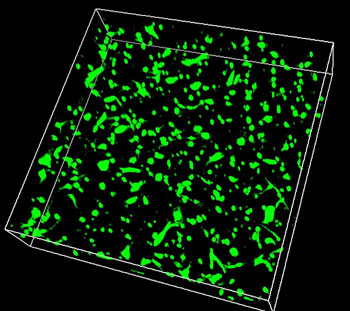
| 3D image of skin cells successfully growing in the biocompatible silk hydrogel. (Image: Siwei Zhao) | |
| In living tissues and organs, interactions with other cells, proteins, and enzymes occur both within the tissue and on the surface of the channels. Modeling this involves embedding living cells and active enzymes within the gel while it’s made. However, the harsh conditions required to create PDMS kill and deactivate cells and enzymes. Because a silk hydrogel can be made at ambient temperatures and under relatively gentle conditions, it can include cells and enzymes within the gel and thus better replicate living tissue. | |
| Silk gels were also able to withstand a variety of environments (such as changes to the surrounding fluid’s pH or salinity) without altering their size or shape. On the other hand, the stiffness of the gel could be manipulated to match the properties of the target tissue (harder for cartilage, but soft for skin or brain, for example). The gels were also clear, allowing for easier analysis. | |
| While testing potential drugs is the likely first application of the silk system, David Kaplan, Ph.D., Stern Family Professor of Engineering at Tufts University and senior author of the paper, is also excited about the possibility of someday growing tissues on chips that can be put into the body. “Silk takes you to the next level because it can be implanted and fully resorbed in vivo,” said Kaplan. | |
| And for researchers looking for a system that can be tailored to a specific need—whether it’s mechanical pumps, cell signaling, or imaging of cellular processes within the chip—this is it, said Kaplan. “Silk is pretty unique in the ability to integrate everything into one material system,” he said. “Now we can optimize systems in vitro (in cell culture) and directly translate that in vivo (within an animal) to look at tissue regeneration. I don’t know of any other system with the versatility that can do all that.” | |
| Kaplan is known for using silk to solve biomedical engineering problems; he’s used it to make models of brain tissue and bone marrow, as part of surgical implants to heal broken bones, and as a method for keeping antibodies and vaccines stable at room temperature. “It’s pretty rare when we hit a roadblock that we can’t overcome with silk as the base material,” said Kaplan. “It’s a fairly universal material. I’m hopeful we’ve moved it out of the textile world and into the biomaterials and medical world.” | |
| Indeed, compared to other polymers being tested, silk is well studied. “We already know a lot about how it reacts inside the body,” said Hunziker. In terms of developing silk-based tissue implants, “It’s like starting a relay race on the last lap instead of from the beginning.” |
| Source: National Institute of Biomedical Imaging and Bioengineering | |
| Subscribe to a free copy of one of our daily Nanowerk Newsletter Email Digests with a compilation of all of the day’s news. |
Graphene, un material minunat bidimensional compus dintr-un singur strat de atomi de carbon legat într-un model hexagonal de sârmă de pui, a atras un interes intens pentru capacitatea sa fenomenală de a conduce electricitatea. Acum, cercetătorii de la Universitatea Illinois din Chicago au folosit bacterii în formă de tijă – aliniate precis într-un câmp electric, apoi sub presiune sub o foaie de grafen – pentru a introduce valuri nanoscale în material, determinând conducerea electronilor diferit în direcții perpendiculare.
Materialul rezultat, un fel de nano-corupru de grafen, poate fi aplicat unui cip de silicon și poate adăuga potențialul aproape nelimitat al lui Grafen în domeniul electronicii și nanotehnologiei. Constatarea este raportată în jurnalul ACS Nano ( „Riduri de tip grafenă anizotrofică, orientată și anizotropică electric pe bacterii” ).Alături de nanotuburi de carbon, grafen și fullerene, acesta este un allotrop carbon nou – un nanotub de jumătate de carbon legat de grafen”, a spus el. „Structura este diferită, iar proprietățile electronice fundamentale sunt noi.”
| Posted: Jul 11, 2016 | |
Germs add ripples to make ‘groovy’ graphene(Nanowerk News) Graphene, a two-dimensional wonder-material composed of a single layer of carbon atoms linked in a hexagonal chicken-wire pattern, has attracted intense interest for its phenomenal ability to conduct electricity. Now University of Illinois at Chicago researchers have used rod-shaped bacteria – precisely aligned in an electric field, then vacuum-shrunk under a graphene sheet – to introduce nanoscale ripples in the material, causing it to conduct electrons differently in perpendicular directions. |
|
| The resulting material, sort of a graphene nano-corduroy, can be applied to a silicon chip and may add to graphene’s almost limitless potential in electronics and nanotechnology. The finding is reported in the journal ACS Nano („Confined, Oriented and Electrically Anisotropic Graphene Wrinkles on Bacteria”). | |
 |
|
| This is an atomic force microscopy image of a graphene sheet draped over a Bacillus bacterium (left). The bacterium is about 1 micron or 1/25,000 of an inch wide. After applying vacuum and heat treatment, regular wrinkles form in the graphene (right, at twice the magnification). (Image: Vikas Berry, University of Illinois at Chicago) | |
| „The current across the graphene wrinkles is less than the current along them,” says Vikas Berry, associate professor and interim head of chemical engineering at UIC, who led the research. | |
| The key to formation of these wrinkles, he said, is graphene’s extreme flexibility at the nanometer scale, which allows formation of carbon nanotubes. | |
| „The wrinkle opens a ‘V’ in the electron cloud around each carbon atom,” Berry said, creating a dipole moment, which can open an electronic band gap that flat graphene does not have. | |
| Other researchers have created wrinkles in graphene by stretching the sheet and letting it snap back. But such wrinkles are not confined in microscale and cannot be directed towards a location on a micro-device, Berry said. | |
| He and his colleagues came up with a unique way to introduce circumscribed, guided, and regular graphene ripples using bacillus bacteria, by using the graphene itself as a check-valve to alter the volume of the cells. | |
| The researchers placed the bacteria in an electric field, causing them to line up like strings of hot dogs in repeating rows. Then they applied a sheet of graphene over the top. | |
| „Under vacuum, the graphene lifts, and lets water out,” Berry said. But under pressure, graphene sits back down on the substrate and prevents water from re-entering the bacteria, he said. | |
| „It’s a nanoscopic valve that actuates unidirectional fluid flow in a microorganism,” Berry said. „Futuristically, this valve operation could be applied to microfluidic devices where we want flow in one direction but not the other.” | |
| After the bacteria have been vacuum-shrunk, the graphene reconforms, but with wrinkles. After heat treatment, the resulting permanent ripples atop the bacteria are all aligned longitudinally, with a height of 7 to 10 nanometers, and a wavelength of about 32 nm. | |
| The wrinkles were observed by field emission scanning electron microscopy, which must be done under high vacuum, and by atomic force microscopy at atmospheric pressure. | |
| „The [ripple] wavelength is proportional to the thickness of the material, and graphene is the thinnest material in the world,” Berry said. „We envision that with graphene one could make the smallest wavelength wrinkles in the world – about 2 nanometers.” | |
| The next goal, he said, will be to create processes to further refine the ripples and vary their amplitude, wavelength and longitudinal length. | |
| To measure the effect of the ripples’ orientation on the carrier transport, graduate student Shikai Deng, the lead author of the paper, fabricated a plus-shaped device with bacteria aligned parallel to one pair of electrodes and perpendicular to another pair. He found the rippled graphene’s conduction barrier was greater in the transverse direction than in the longitudinal direction. | |
| The introduction of oriented ripples to graphene represents an entirely new material, Berry said. | |
| „Along with carbon nanotubes, graphene and fullerene, this is a new carbon allotrope – a half carbon nanotube linked to graphene,” he said. „The structure is different, and the fundamental electronic properties are new.” |
| Source: University of Illinois at Chicago |
Read more: Germs add ripples to make ‘groovy’ graphene
Echipele de răspuns bine instruite funcționează în medii dinamice și provocatoare, în medii urbane, rurale sau în sălbăticie;Robot multi-propunere;acceptă de asemenea un volum util opțional pentru afișarea imaginilor prin satelit a locației robotului și a căii de parcurs, completată cu coordonatele de distanță și GPS
cel mai bun tricou ARB-15 / M4 / M4A1 cu carabină / pușcă cu șurub scurt (SBR) Bolt Carrier Group
bomba robot;pentru a implementa un robot ca o armă a fost repetată, dar nu a fost prezentată niciodată șerifului;
Noul detector funcționează la o suta de grade deasupra temperaturii zero absolute. Perturbațiile termice la temperaturi atât de scăzute sunt atât de slabe încât echipa de cercetare ar putea detecta pachete energetice de numai un singur zeptojoule. Aceasta este energia necesară pentru ridicarea unei celule roșii din sânge cu un singur nanometru.
Cea de-a doua dezvoltare-cheie se referă la amplificarea semnalului rezultat din micile pachete de energie. În acest scop, oamenii de știință au folosit ceva numit feedback pozitiv. Aceasta înseamnă că există o sursă externă de energie care amplifică schimbările de temperatură care decurg din fotonii absorbiți.
| Posted: Jul 08, 2016 | |
New record in microwave detection(Nanowerk News) Aalto University scientists have broken the world record by fourteen fold in the energy resolution of thermal photodetection. |
|
| The record was made using a partially superconducting microwave detector. The discovery may lead to ultrasensitive cameras and accessories for the emerging quantum computer. | |
 |
|
| Figure 1: Artistic image of a hybrid superconductor-metal microwave detector. (Image: Ella Maru Sudio) The first of the two key enabling developments is the new detector design consisting of tiny pieces of superconducting aluminum and a golden nanowire. This design guarantees both efficient absorption of incoming photons and very sensitive readout. The whole detector is smaller than a single human blood cell. | |
| “For us size matters. The smaller the better. With smaller detectors, we get more signal and cheaper price in mass production”, says Mikko Möttönen, the leader of the record-breaking Quantum Computing and Devices research group. | |
| The new detector works at a hundredth of a degree above absolute zero temperature. Thermal disturbances at such low temperatures are so weak that the research team could detect energy packets of only a single zeptojoule. That is the energy needed to lift a red blood cell by just a single nanometer. | |
| The second key development concerns the amplification of the signal arising from the tiny the energy packets. To this end, the scientists used something called positive feedback. This means that there is an external energy source that amplifies the temperature change arising from the absorbed photons. | |
 |
|
| Figure 2: Scanning-electron microscope image of the microwave detector. The nanowire is colored yellow and the other parts are superconducting aluminum. Photons arrive from the left and get absorbed at the long part of the nanowire. This leads to an elevated temperature and weakening of superconductivity at the short parts of the nanowire which consequently work as a sensitive thermometer. (Image: Joonas Govenius) | |
| From discovery to products | |
| Microwaves are currently used in mobile phone communications and satellite televisions, thanks to their ability to pass through walls. More sensitive microwave detectors may lead to great improvements of the present communication systems and measurement techniques. | |
| The European Research Council (ERC) has just awarded Möttönen a prestigious Proof of Concept Grant to develop the detector towards commercial applications. This was the third personal ERC grant awarded to Möttönen. | |
| Besides communication systems the new detector could be used as a measurement device in the emerging superconducting quantum computer. | |
| “Existing superconducting technology can produce single microwave photons. However, detection of such traveling photons efficiently is a major outstanding challenge. Our results provide a leap towards solving this problem using thermal detection,” says Joonas Govenius who is the first author of the work (Physical Review Letters, „Detection of zeptojoule microwave pulses using electrothermal feedback in proximity-induced Josephson junctions”). | |
| New Physics | |
| A microwave detector may also be useful for thermodynamics of small systems, a new research area Möttönen has studied in collaboration with his Aalto colleague Professor Jukka Pekola. | |
| Now Pekola and his group want to go to the quantum regime but they first need a detector capable of measuring the energy released by the quantum systems. This means that the detector should be able to accurately measure single microwave photons. | |
| “Quantum thermodynamics may give yet another boost to technology since it deals with individual energy levels or particles, and is in this sense more precise than classical thermodynamics”, says Möttönen. | |
| “There are also other groups developing single-photon microwave detectors such as that of Pekola. This is great since we can learn from each other and this way come up with even better products for future end users”, concludes Möttönen. |
| Source: Aalto University | |
Read more: New record in microwave detection
detectare amenintari chimice