Un viitor colorat luminat de fizica mistificatoare a semiconductorilor cu vopsea(

Unele materiale romantice care sună prea bine pentru a fi adevărate se dovedesc a fi adevărate și bune. O clasă emergentă de semiconductori, care ar putea lumina viitorul nostru cu culori nuanțate provenite din lasere, lămpi și chiar geamuri, ar putea fi ultimul exemplu.
Aceste materiale sunt foarte radiante, ușor de procesat din soluție și eficiente din punct de vedere energetic.Biexcitonii se ridică energic pentru a absorbi energia de intrare. Apoi se contractă energic și pompează lumina. Acest lucru ar funcționa nu numai la lasere, ci și la LED-uri sau alte suprafețe care utilizează materialul optoelectronic.

Posted: Mar 19, 2018

A future colorfully lit by mystifying physics of paint-on semiconductors

(Nanowerk News) Some novel materials that sound too good to be true turn out to be true and good. An emergent class of semiconductors, which could affordably light up our future with nuanced colors emanating from lasers, lamps, and even window glass, could be the latest example.

These materials are very radiant, easy to process from solution, and energy-efficient. The nagging question of whether hybrid organic-inorganic perovskites (HOIPs) could really work just received a very affirmative answer in a new international study led by physical chemists at the Georgia Institute of Technology.
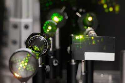
Laser light in the visible range in a lab set-up
Laser light in the visible range is processed for use in the testing of quantum properties in materials in Carlos Silva’s lab at Georgia Tech. (Image: Allison Carter, Georgia Tech)
The researchers observed in an HOIP a “richness” of semiconducting physics created by what could be described as electrons dancing on chemical underpinnings that wobble like a funhouse floor in an earthquake. That bucks conventional wisdom because established semiconductors rely upon rigidly stable chemical foundations, that is to say, quieter molecular frameworks, to produce the desired quantum properties.
“We don’t know yet how it works to have these stable quantum properties in this intense molecular motion,” said first author Felix Thouin, a graduate research assistant at Georgia Tech. “It defies physics models we have to try to explain it. It’s like we need some new physics.”

Quantum properties surprise

Their gyrating jumbles have made HOIPs challenging to examine, but the team of researchers from a total of five research institutes in four countries succeeded in measuring a prototypical HOIP and found its quantum properties on par with those of established, molecularly rigid semiconductors, many of which are graphene-based.
“The properties were at least as good as in those materials and may be even better,” said Carlos Silva, a professor in Georgia Tech’s School of Chemistry and Biochemistry. Not all semiconductors also absorb and emit light well, but HOIPs do, making them optoelectronic and thus potentially useful in lasers, LEDs, other lighting applications, and also in photovoltaics.
The lack of molecular-level rigidity in HOIPs also plays into them being more flexibly produced and applied.
Silva co-led the study with physicist Ajay Ram Srimath Kandada. Their team published the results of their study on two-dimensional HOIPs in the journal Physical Review Materials („Stable biexcitons in two-dimensional metal-halide perovskites with strong dynamic lattice disorder”). Their research was funded by EU Horizon 2020, the Natural Sciences and Engineering Research Council of Canada, the Fond Québécois pour la Recherche, the Research Council of Canada, and the National Research Foundation of Singapore.

The ‘solution solution’

Commonly, semiconducting properties arise from static crystalline lattices of neatly interconnected atoms. In silicon, for example, which is used in most commercial solar cells, they are interconnected silicon atoms. The same principle applies to graphene-like semiconductors.
“These lattices are structurally not very complex,” Silva said. “They’re only one atom thin, and they have strict two-dimensional properties, so they’re much more rigid.”
“You forcefully limit these systems to two dimensions,” said Srimath Kandada, who is a Marie Curie International Fellow at Georgia Tech and the Italian Institute of Technology. “The atoms are arranged in infinitely expansive, flat sheets, and then these very interesting and desirable optoelectronic properties emerge.”
These proven materials impress. So, why pursue HOIPs, except to explore their baffling physics? Because they may be more practical in important ways.
“One of the compelling advantages is that they’re all made using low-temperature processing from solutions,” Silva said. “It takes much less energy to make them.”
By contrast, graphene-based materials are produced at high temperatures in small amounts that can be tedious to work with. “With this stuff (HOIPs), you can make big batches in solution and coat a whole window with it if you want to,” Silva said.

Funhouse in an earthquake

For all an HOIP’s wobbling, it’s also a very ordered lattice with its own kind of rigidity, though less limiting than in the customary two-dimensional materials.
“It’s not just a single layer,” Srimath Kandada said. “There is a very specific perovskite-like geometry.” Perovskite refers to the shape of an HOIPs crystal lattice, which is a layered scaffolding.
“The lattice self-assembles,” Srimath Kandada said, “and it does so in a three-dimensional stack made of layers of two-dimensional sheets. But HOIPs still preserve those desirable 2D quantum properties.”
Those sheets are held together by interspersed layers of another molecular structure that is a bit like a sheet of rubber bands. That makes the scaffolding wiggle like a funhouse floor.
“At room temperature, the molecules wiggle all over the place. That disrupts the lattice, which is where the electrons live. It’s really intense,” Silva said. “But surprisingly, the quantum properties are still really stable.”
Having quantum properties work at room temperature without requiring ultra-cooling is important for practical use as a semiconductor.
Going back to what HOIP stands for – hybrid organic-inorganic perovskites – this is how the experimental material fit into the HOIP chemical class: It was a hybrid of inorganic layers of a lead iodide (the rigid part) separated by organic layers (the rubber band-like parts) of phenylethylammonium (chemical formula (PEA)2PbI4).
The lead in this prototypical material could be swapped out for a metal safer for humans to handle before the development of an applicable material.

Electron choreography

HOIPs are great semiconductors because their electrons do an acrobatic square dance.
Usually, electrons live in an orbit around the nucleus of an atom or are shared by atoms in a chemical bond. But HOIP chemical lattices, like all semiconductors, are configured to share electrons more broadly.
Energy levels in a system can free the electrons to run around and participate in things like the flow of electricity and heat. The orbits, which are then empty, are called electron holes, and they want the electrons back.
“The hole is thought of as a positive charge, and of course, the electron has a negative charge,” Silva said. “So, hole and electron attract each other.”
The electrons and holes race around each other like dance partners pairing up to what physicists call an “exciton.” Excitons act and look a lot like particles themselves, though they’re not really particles.

Hopping biexciton light

In semiconductors, millions of excitons are correlated, or choreographed, with each other, which makes for desirable properties, when an energy source like electricity or laser light is applied. Additionally, excitons can pair up to form biexcitons, boosting the semiconductor’s energetic properties.
“In this material, we found that the biexciton binding energies were high,” Silva said. “That’s why we want to put this into lasers because the energy you input ends up to 80 or 90 percent as biexcitons.”
Biexcitons bump up energetically to absorb input energy. Then they contract energetically and pump out light. That would work not only in lasers but also in LEDs or other surfaces using the optoelectronic material.
“You can adjust the chemistry (of HOIPs) to control the width between biexciton states, and that controls the wavelength of the light given off,” Silva said. “And the adjustment can be very fine to give you any wavelength of light.”
That translates into any color of light the heart desires.
Source: By Ben Brumfield, Georgia Institute of Technology

Explozie lumina asupra misterului domului supraconductor(Shedding light on the mystery of the superconducting dome)

au indus supraconductivitatea într-un monostrat de disulfură de tungsten. Folosind un câmp electric în creștere, au fost capabili să arate cum se transformă materialul dintr-un izolator într-un superconductor și apoi din nou într-un izolator „reintrant”. Această descoperire ar putea deschide calea pentru proiectarea rațională a dispozitivelor superconductoare 2D care funcționează la temperaturi relativ ridicate.

Posted: Mar 19, 2018

Shedding light on the mystery of the superconducting dome

(Nanowerk News) University of Groningen physicists, and colleagues from Nijmegen and Hong Kong, have induced superconductivity in a monolayer of tungsten disulfide. By using an increasing electric field, they were able to show how the material turns from an insulator into a superconductor and then back into a ‘re-entrant’ insulator again. Their results show the typical ‘dome-shaped’ superconducting phase, and finally provide an explanation for this phenomenon.

The results were published in Proceedings of the National Academy of Sciences („Full superconducting dome of strong Ising protection in gated monolayer WS2„).
The scientists, led by University of Groningen associate professor Justin Ye, used an electric field to induce superconductivity in a monolayer of the semiconductor tungsten disulfide (WS2). In the initial state with very few carriers, the WS2 behaves as an insulator. ‘Basically, the electric field adds carriers to this normal band insulator, which increases the conductivity’, explains Ye. At low temperatures, this initiates a superconducting state.

Temperature

In the superconducting phase, the temperature at which superconductivity occurs rises as the electric field increases before dropping again. This kind of dome-shaped curve has been observed in many superconductors over several decades. It is one of the hallmarks of high temperature superconductors, many mysteries of which remain to be explained. A similar dome was recently also observed in several superconductors that were induced or controlled by field effect. What Ye and his colleagues observed was that, as the electric field increases even further, the system goes from superconductor back to insulator again.
‘This full range for the phase diagram, from insulator to superconductor and then to re-entry insulator, had never before been observed this clearly’, says Ye. ‘We managed it, because we worked with a truly 2D material and used ionic liquid to create an electric field that is much stronger than what is usually applied.’ Normally, as more carriers are added to a bulk or quasi-2D system, the electric field is eventually blocked. Ye: ‘But in a WS2 monolayer, our stronger field can still pass through, which is why we were able to observe the entire range and eventually reach the insulating phase.’

Counterintuitive

This allowed them to draw conclusions on why the different phases appear. ‘What we suggest is that the charge carriers in the material eventually become localized by the high electric field. Thus, they can no longer move through the material and it becomes an insulator.’ This is very counterintuitive, Ye adds: ‘People normally believe that higher gating means more carriers, hence more metallic behaviour.’ This discovery could pave the way for the rational design of 2D superconducting devices that function at relatively high temperatures. ‘Understanding is the first step to controlling the properties of materials for devices’, concludes Ye.
Source: University of Groningen

Un nou tip de biți cuantic în două dimensiuni(A new kind of quantum bits in two dimensions)

Două materiale noi, fiecare compus dintr-un singur strat atomic și vârful unui microscop de scanare – acestea sunt ingredientele pentru a crea un nou tip de așa numitul „punct cuantic”. Aceste nanostructuri extrem de mici permit controlul delicat al electronilor individuali prin reglarea fină a nivelului lor de energie direct. Astfel de dispozitive sunt esențiale pentru tehnologiile cuantice moderne.

Posted: Mar 19, 2018

A new kind of quantum bits in two dimensions

(Nanowerk News) Two novel materials, each composed of a single atomic layer and the tip of a scanning tunneling microscope – these are the ingredients to create a novel kind of a so-called „quantum dot”. These extremely small nanostructures allow delicate control of individual electrons by fine-tuning their energy levels directly. Such devices are key for modern quantum technologies.

The theoretical simulations for the new technology were performed in the team of Prof. Florian Libisch and Prof. Joachim Burgdörfer at TU Wien. The experiment involved the group of Prof. Markus Morgenstern at RWTH Aachen and the team around Nobel-prize laureates Andre Geim and Kostya Novoselov from Manchester who prepared the samples. The results have now been published in Nature Nanotechnology („Large tunable valley splitting in edge-free graphene quantum dots on boron nitride”).
text
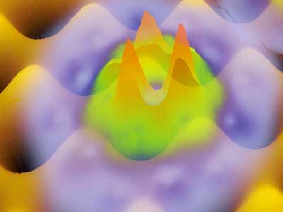
New kinds of quantum bits: Tiny nanostructures allow delicate control of individual electrons. (Image: TU Vienna)

Tuning electron energies

„For many applications in the field of quantum technologies one requires a quantum system were electrons occupy two states – similar to a classical switch – on or off, with the difference that quantum physics also allows for arbitrary superpositions of the on and off states” explains Florian Libisch from the Institute for Theoretical Physics at TU Wien.
A key property of such systems is the energy difference between those two quantum states: „Efficiently manipulating the information stored in the quantum state of the electrons requires perfect control of the system parameters. An ideal system allows for continuous tuning the energy difference from zero to a large value” says Libisch.
For systems found in nature – for example atoms – this is usually difficult to realize. The energies of atomic states, and hence their differences, are fixed. Tuning energies becomes possible in synthetic nanostructures engineered towards confining electrons. Such structures are often referred to as quantum dots or „artificial atoms”.

Two ultra-thin materials: graphene and hexagonal boron nitride

The international research team of TU Wien, RWTH Aachen and the University of Manchester now succeeded in developing a new type of quantum dots which allow for much more accurately and widely tunable energy levels of confined electrons than before. This progress was made possible by combining two very special materials: graphene, a conductive single atomic layer of carbon atoms, and hexagonal boron nitride, also a single layer of material quite similar to graphene except that it is insulating.
Exactly like graphene boron nitride also forms a honeycomb lattice. „The honeycombs in graphene and hexagonal boron nitride are, however, not exactly of equal size” explains Florian Libisch. „If you carefully put a single layer of graphene on top of hexagonal boron nitride, the layers cannot perfectly match. This slight mismatch creates a superstructure over distances of several nanometers, which results in an extremely regular wave-like spatial oscillation of the graphene layer out of the perfect plane.”
As the extensive simulations at TU Wien show, exactly these oscillations in graphene on hexagonal boron nitride form the ideal scaffold to control electron energies. The potential landscape created by the regular superstructure allows for accurately placing the quantum dot, or even moving it continuously and thus smoothly changing its properties. Depending on the exact position of the tip of the scanning tunneling microscope, the energy levels of the electronic states inside the quantum dot change. „A shift by a few nanometers allows for changing the energy difference of two neighboring energy levels from minus five to plus ten millielectronvolts with high accuracy – a tuning range about fifty times larger than previously possible”, explains Florian Libisch.

Towards „Valleytronics”

As a next step, the tip of the scanning tunneling microscope could be replaced by a series of nanoelectronic gates. This would allow for exploiting the quantum dot states of graphene on hexagonal boron nitride for scalable quantum technologies such as „valleytronics”.
„This emerging new field is quickly becoming a center of attention”, comments Florian Libisch. „There are multiple potential technological applications of these atomically thin materials – that is also why the TU Wien has also very recently established a special doctoral college focused on two-dimensional materials.”
Source: Vienna University of Technology

Forțele viitoare să utilizeze inelul compact pentru detectarea amenințărilor chimice(Future Forces to Use Compact Ring for Chemical Threat Detection )

Cererea de senzori compacți, ușori și portabili, care au capacitatea de a se conecta la smartphone-uri și laptopuri sau computere, este în creștere

Future Forces

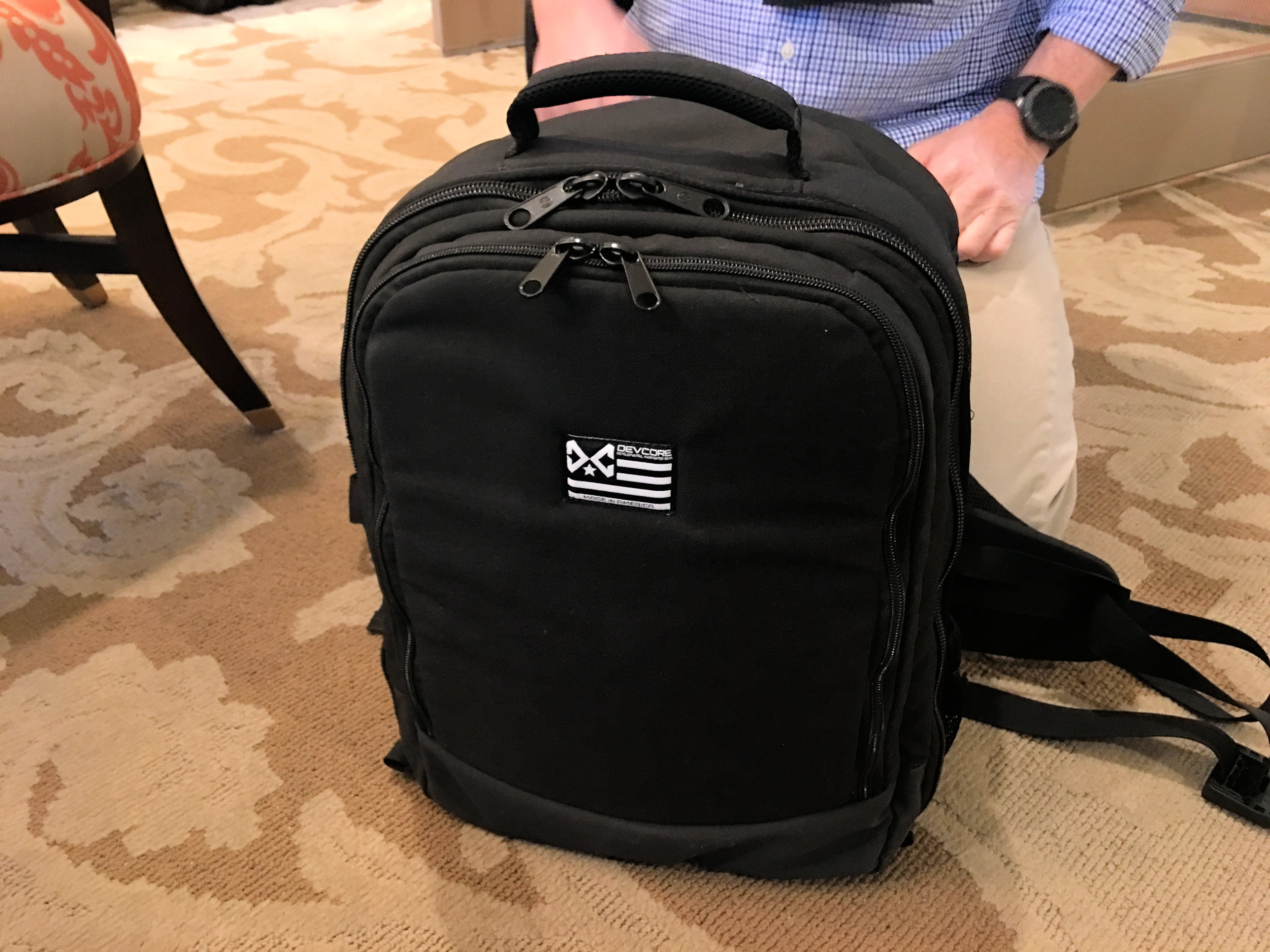
Rucsac:tactical Body Armor și pistolul pe țintă în câteva secunde!Aparatul Devcore Deploy On Attack (DOA) Plate de rucsac Carrier Pack Prototype: Instant Anti-Rifle Combat / Tactical Body Armor și pistolul pe țintă în câteva secunde!(Devcore Deploy On Attack (DOA) Backpack Plate Carrier Pack Prototype: Instant Anti-Rifle Combat/Tactical Body Armor, and Gun on Target in Seconds!)

A doua caracteristică cea mai mare în afara desfășurării armurii ar fi capacitatea de a avea un pistol fixat pe același purtător de placă frontală care merge de la ascunderea totală la arma pe țintă în mai puțin de 2,5 secunde. Se rupe până la 1,5 secunde pentru a desface transportatorul de plăci și o secundă pentru a avea pistolul pe piept pe țintă. Am dezvoltat o cutie de lacrimă care nu numai că ține pistolul sigur în timpul desfășurării plăcii frontale, dar are de asemenea o caracteristică deschisă la rupere, care vă permite să ajungeți la pistol în jumătate de secundă.

Devcore Deploy On Attack (DOA) Backpack Plate Carrier Pack Prototype: Instant Anti-Rifle Combat/Tactical Body Armor, and Gun on Target in Seconds! (Video!)

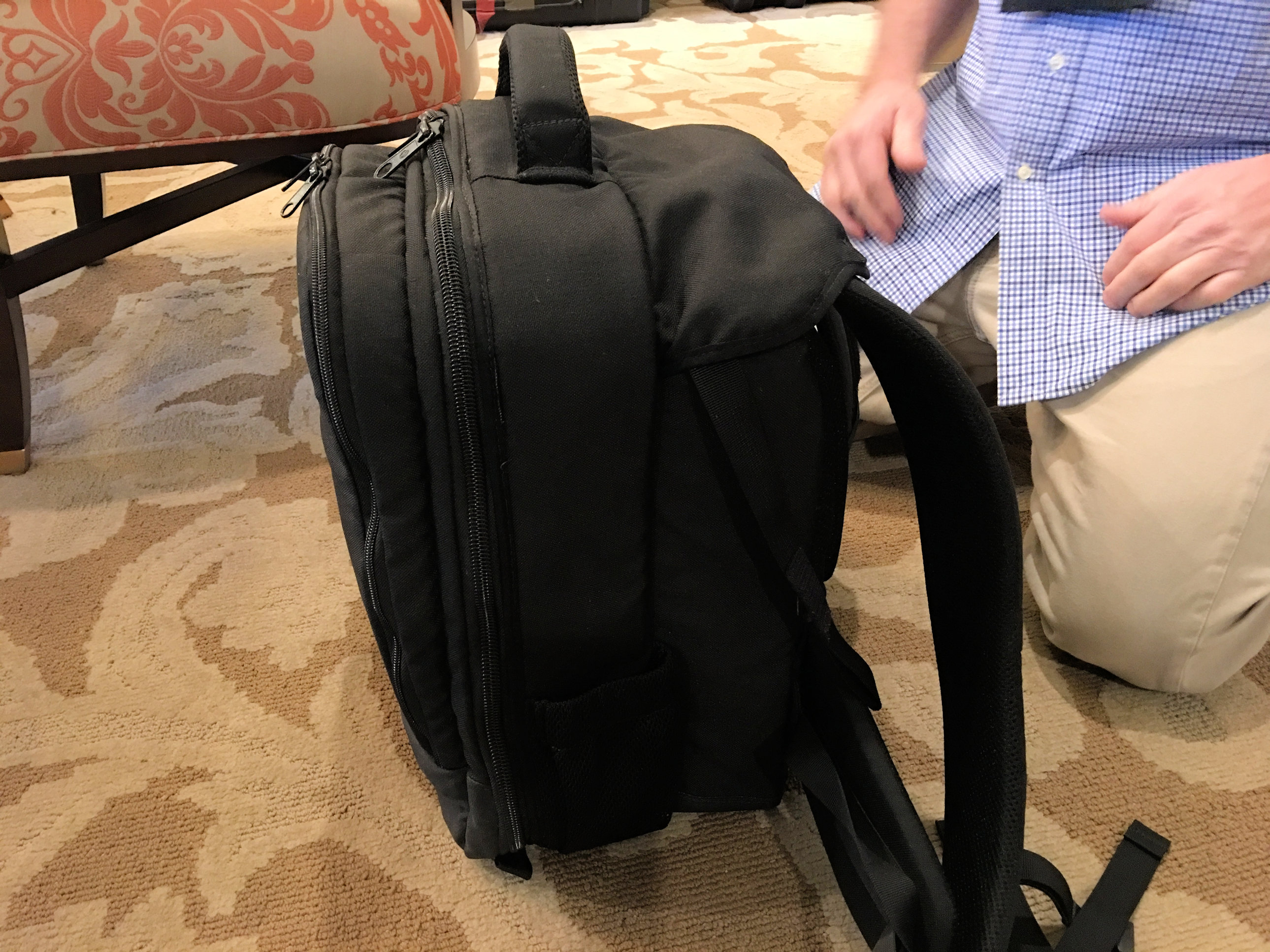
DefenseReview (DR) recently got to see an extremely cool new (patented) plate carrier pack prototype designed and developed by a brand new tactical-gear startup company called Devcore at SHOT Show 2018, and it really blew us away. It’s called the Deploy On Attack (DOA) Backpack, and as you can see in DR’s short video below, it deploys in seconds (WITHOUT having to open the pack!), turning the pack into instant anti-rifle body armor. Oh, and it also allows you to quickly draw a concealed pistol from the Velcro-sealed front plate/chest compartment (via a pull-tab, we believe) as soon as you’ve deployed it, and be on target in under 2.5 seconds. It’s pretty badass. And, it’s a game-changer for lo-pro/lo-vis (low-profile/low-visibility military special operations forces (SOF) missions.

Devcore’s Brian Miller just sent DR all the juicy details on the pack, as follows:

“Devcore DOA (Deploy On Attack) Backpack

This backpack is a deployable concealment armor system. It turns a standard looking backpack into a full front and back plates rig in under 1.5 seconds from time of action. Unlike other bags that require your to remove the backpack to set it up and put it back on, this system allows you to simply pull two straps on the backpack shoulder straps to deploy a full front plate carrier into secure position. The back plate is built into a hidden sleeve in the backpack itself. You are now fully armored up in under 1.5 seconds, going from a guy wearing nothing more than a standard looking backpack, to a fully armored personal ready to stand up to a high caliber ballistic threat.

The second biggest feature outside of the armor deployment, would be the capability to have a handgun fixed to this same front plate carrier that goes from total concealment to gun on target in less than 2.5 seconds. It breaks down to 1.5 seconds to deploy plate carrier and one second to have gun off chest on target. We developed a tear pouch that not only holds the gun secure during front plate deployment, but also has a tear open feature that allows you to get to the gun in half a second. We guarantee that no other concealed armor system on the market can go from backpack to full plate protection with gun on target in under 2.5 seconds.

One other note, your backpack itself never has to be opened during the deployment of the plate system.

The DOA system is under patent, and we’re currently developing the actual backpack portion to be able to zip on and off different compartment configurations such as a Medic bag, sub gun bag, standard backpack set-up, etc. We are very excited to get this system to market as it will be a game changer for Low-Vis LE and Military operations.”

The (prototype) Devcore DOA Backpack plate carrier pack is really an amazing design. It’s honestly one of the coolest pieces of combat/tactical gear Defense Review has ever seen. so we can’t wait to see the production version(s) of it. We should also note that the DOA pack is going to be made right here in America (USA), so it’ll be Berry Compliant, and of the highest quality of manufacture.


Company Contact Info:

Brian Miller
Devcore
Phone: 323-899-3016
Email: [email protected]

Nanoscale particule de livrare de droguri, care pot simti imprejurimile lor(Nanoscale drug delivery particles that can sense their surroundings)

Noile nanoparticule dezvoltate de Zibiao Li de la Institutul de Materiale de Cercetare și Inginerie A * STAR și colaboratorii săi, reprezintă un upgrade semnificativ față de generațiile anterioare de nanoparticule de eliberare a medicamentelor pe bază de polimeri. Exemplele timpurii constau în mod obișnuit din lanțuri simple de polimeri cu un cap polar, hidrofil și o coadă nepolară, hidrofobă. În apă, aceste lanțuri se agregă în mod natural în sfere, cu cozile lor hidrofobe toate îndreptate spre interior pentru a forma un nucleu nepolar. Miezul a format un loc bun pentru ca moleculele de droguri să se încadreze. În sânge, cu toate acestea, aceste agregate tind să fie rupte.

Posted: Mar 16, 2018

Nanoscale drug delivery particles that can sense their surroundings

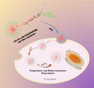
(Nanowerk News) A*STAR researchers have developed nanoscale drug delivery particles that can sense their surroundings, and release their payload only after entering a cell, a discovery that could make many existing medicines more effective (Polymer Chemistry, „“Y”-shape armed amphiphilic star-like copolymers: design, synthesis and dual-responsive unimolecular micelle formation for controlled drug delivery”).

The new nanoparticles, developed by Zibiao Li from the A*STAR Institute of Materials Research and Engineering and his collaborators, are a significant upgrade from previous generations of polymer-based drug delivery nanoparticles. Early examples typically consisted of simple polymer chains with a polar, hydrophilic head and a non-polar, hydrophobic tail. In water, these chains naturally aggregate into spheres, with their hydrophobic tails all pointing inward to form a non-polar core. The core formed a good site for drug molecules to nestle. In the bloodstream, however, these aggregates tend to be torn apart.
The change in temperature and chemical environment inside the cell triggers the nanoparticle to release its drug payload
The change in temperature and chemical environment inside the cell triggers the nanoparticle to release its drug payload. (© RSC)
Li and his colleagues used the latest polymer synthesis techniques to create single-molecule nanoparticles. Rather than a self-assembled aggregate of separate polymers, the team synthesized a more robust structure in which the polymer chains were strongly covalently bonded to a central core. The synthesis began with beta-cyclodextrin, a circular sugar molecule with 21 hydroxyl groups on its surface. The hydroxyl groups formed the chemical anchors from which the team constructed the nanoparticle’s multiple long, Y-shaped, multifunctional polymer arms.
“The greatest challenge in making the [nanoparticle] was to integrate different synthetic methodologies into one macromolecular design,” says Li. At one of the ends of each Y-shaped branch, the team attached a temperature-sensitive polymer called PNIPAM. At room temperature the PNIPAM polymer extends outward, but collapses once body temperature, 37 degrees Celsius, is reached, allowing the nanoparticle’s drug molecule cargo to escape.
Mid-way along each polymer arm, the team installed a sulfur-sulfur bond. When the particles enter a cell, they meet high levels of glutathione, a molecule that cleaves sulfur-sulfur bonds. Thus the nanoparticle’s outer polymer coat is snipped off, and the drug is released even faster.
When the team tested this effect with an anti-cancer drug called doxorubicin, the dual-action effect was clear. “The change from room temperature to body temperature, and the effect of glutathione, showed synergistic and fast release of the drug,” Li says. At lower temperatures, or in the absence of glutathione, drug release was significantly slower, he says.
“The next plan is to integrate new functionality, for precision release of the drug for targeted cancer therapy,” says Li. One end of each Y-shaped branch could be functionalized with a molecule that sticks selectively to cancer cells, delivering the drug precisely where it is needed.
Source: A*STAR

Ultra-alb nanocoating modelate pe scale scaun(Ultra-white nanocoating modelled on beetle scales)

Materialul – de 20 de ori mai alb decât hârtia – este fabricat din celuloză netoxică și atinge o alunecare atât de strălucitoare, imitând structura cântarelor ultra-subțiri ale anumitor tipuri de gândaci.Ca și cântarele de gândac, membranele de celuloză sunt extrem de subțiri: doar câteva milimi de un metru gros, deși cercetătorii spun că membranele chiar mai subțiri ar putea fi produse prin optimizarea în continuare a procesului lor de fabricare. Membranele împrăștie lumina de 20 până la 30 de ori mai eficient decât hârtia și ar putea fi utilizate pentru a produce materiale de lumină durabile și biologice compatibile de generație viitoare de ultimă generație.

Posted: Mar 15, 2018

Ultra-white nanocoating modelled on beetle scales

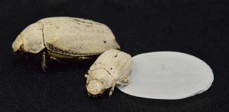
(Nanowerk News) The material – which is 20 times whiter than paper – is made from non-toxic cellulose and achieves such bright whiteness by mimicking the structure of the ultra-thin scales of certain types of beetle. The results are reported in the journal Advanced Materials („Anomalous-Diffusion-Assisted Brightness in White Cellulose Nanofibril Membranes”).

Bright colours are usually produced using pigments, which absorb certain wavelengths of light and reflect others, which our eyes then perceive as colour.
To appear as white, however, all wavelengths of light need to be reflected with the same efficiency. Most commercially-available white products – such as sun creams, cosmetics and paints – incorporate highly refractive particles (usually titanium dioxide or zinc oxide) to reflect light efficiently. These materials, while considered safe, are not fully sustainable or biocompatible.
Cyphochilus beetle with cellulose-based coating
Cyphochilus beetle with cellulose-based coating. (Image: Olimpia Onelli)
In nature, the Cyphochilus beetle, which is native to Southeast Asia, produces its ultra-white colouring not through pigments, but by exploiting the geometry of a dense network of chitin – a molecule which is also found in the shells of molluscs, the exoskeletons of insects and the cell walls of fungi. Chitin has a structure which scatters light extremely efficiently – resulting in ultra-white coatings which are very thin and light.
“White is a very special type of structural colour,” said paper co-author Olimpia Onelli, from Cambridge’s Department of Chemistry. “Other types of structural colour – for example butterfly wings or opals – have a specific pattern in their structure which results in vibrant colour, but to produce white, the structure needs to be as random as possible.”
The Cambridge team, working with researchers from Aalto University in Finland, mimicked the structure of chitin using cellulose, which is non-toxic, abundant, strong and bio-compatible. Using tiny strands of cellulose, or cellulose nanofibrils, they were able to achieve the same ultra-white effect in a flexible membrane.
By using a combination of nanofibrils of varying diameters, the researchers were able to tune the opacity, and therefore the whiteness, of the end material. The membranes made from the thinnest fibres were more transparent, while adding medium and thick fibres resulted in a more opaque membrane. In this way, the researchers were able to fine-tune the geometry of the nanofibrils so that they reflected the most light.
“These cellulose-based materials have a structure that’s almost like spaghetti, which is how they are able to scatter light so well,” said senior author Dr Silvia Vignolini, also from Cambridge’s Department of Chemistry. “We need to get the mix just right: we don’t want it to be too uniform, and we don’t want it to collapse.”
Like the beetle scales, the cellulose membranes are extremely thin: just a few millionths of a metre thick, although the researchers say that even thinner membranes could be produced by further optimising their fabrication process. The membranes scatter light 20 to 30 times more efficiently than paper and could be used to produce next-generation efficient bright sustainable and biocompatible white materials.
Source: University of Cambridge

Noul lichid de centrifugare cuantic previzionat de Premiul Nobel pentru prima data(New quantum spin liquid predicted by Nobel Laureate prepared for the first time)

Supraconductoarele de temperatură ridicată sunt oxizi de cupru în care ionii de cupru formează o latură pătrată, astfel încât momentele magnetice adiacente se confruntă în direcții opuse. Când această structură este deranjată de modificarea stării de oxidare a cuprului, materialul devine supraconductor. În noile cercetări publicate acum, interacțiunile magnetice ale acestei structuri pătrate au fost modificate cu ioni cu o structură electronică d10 și d0, care a transformat materialul într-un lichid cu spin quantum

Posted: Mar 15, 2018

New quantum spin liquid predicted by Nobel Laureate prepared for the first time

(Nanowerk News) In 1987 Paul W. Anderson, a Nobel Prize winner in Physics, proposed that high-temperature superconductivity, or loss of electrical resistance, is related to an exotic quantum state now known as quantum spin liquid. Magnetic materials are made up of very tiny magnets, which can be as small as individual electrons. The strength and direction of these are described by the magnetic moment.

In quantum spin liquids, magnetic moments behave like a liquid and do not freeze or order even at absolute zero. These quantum states are being studied as promising materials for new, so-called topological quantum computers, in which operations are based on particle-like excited states found in quantum spin liquids.
In addition to large computational power, a topological quantum computer is characterised by high fault tolerance, which makes it possible to increase the size of the computer.
However, only a few quantum spin liquids suitable for topological quantum computers have been identified so far.
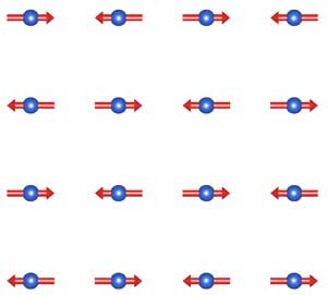
magnetically ordered square lattice of copper ions
The magnetically ordered square lattice of copper ions. Tailoring the structure caused the formation of quantum spin liquid. Modifying the structure in a different way results in high-temperature superconductivity. (Image: Otto Mustonen)

A method of tailoring the magnetism of materials developed at Aalto enabled the preparation of a new quantum spin liquid

Now, for the first time ever, researchers from Aalto University, Brazilian Center for Research in Physics (CBPF), Technical University of Braunschweig and Nagoya University have produced the superconductor-like quantum spin liquid predicted by Anderson.
This is an important step towards understanding superconductors and quantum materials. The preparation of a quantum spin liquid was made possible by a new way of tailoring the properties of magnetic materials that was developed by chemists at Aalto University. The results of the research have been published in Nature Communications („Spin-liquid-like state in a spin-1/2 square-lattice antiferromagnet perovskite induced by d10–d0 cation mixing”).
High-temperature superconductors are copper oxides in which the copper ions form a square lattice so that the adjacent magnetic moments face in opposite directions. When this structure is disturbed by changing the oxidation state of copper, the material becomes superconducting. In the new research now published, the magnetic interactions of this square structure were modified with ions with a d10 and d0 electronic structure, which turned the material into a quantum spin liquid.
“In the future, this new d10/d0 method can be utilised in many other magnetic materials, including various quantum materials”, envisions Doctoral Candidate Otto Mustonen from Aalto University.

Seamless cooperation

Empirical detection of quantum spin liquids is difficult and requires extensive research infrastructure.
muon spin spectrometer
The muon spin spectrometer used in the study at the Paul Scherrer Institute. The sample being studied is placed in the cryostat located in the middle, and a muon beam is aimed at it from the back left direction. (Image: Otto Mustonen)
“We used muon spin spectroscopy in the this study. This method is based on the interaction of very short-lived, electron-like elementary particles, known as muons, with the material being studied. The method can detect very weak magnetic fields in quantum materials”, says Professor F. Jochen Litterst from the Technical University of Braunschweig. The measurements were performed at the Paul Scherrer Institute in Switzerland.
“In addition to top-class equipment, the research requires seamless cooperation between chemists and physicists”, emphasises Professor Maarit Karppinen. “We’re going to need the same international multidisciplinary approach in the future so that this research on quantum spin liquids can lead us to the experimental realization of the topological quantum computer.”
Source: Aalto University

Suprafețe rapide(Speedy surfaces)

Utilizarea potențială a suprafețelor care sunt super-lichide-respingătoare, de la textile de protecție și autocurățare, ochelari și ferestre pentru dispozitive medicale și membrane de schimb gazos. Aplicațiile de acoperiri rezistentă la lichide depind nu numai de proprietățile lor de umectare, ci și de transparența, robustețea și costul și viteza de fabricație. Pe lângă faptul că este superperceptiv împotriva lichidelor, această nouă acoperire prezintă o transparență ridicată și rezistă la impactul asupra uleiurilor și picăturilor de apă cu viteză mare.Deoarece timpul de expunere al substratului la flacără este extrem de scurt, pot fi acoperite chiar materiale foarte inflamabile cum ar fi hârtia și lemnul.

Posted: Mar 15, 2018

Speedy surfaces

(Nanowerk News) Researchers from the Max Planck Institute for Polymer Research in Mainz, Germany, and the Tampere University of Technology, Finland, have found a new way of applying a structured coating for liquid repellency (Advanced Materials, „Ultrafast Processing of Hierarchical Nanotexture for a Transparent Superamphiphobic Coating with Extremely Low Roll-Off Angle and High Impalement Pressure”).

By using liquid flame spray, the method is extremely fast. Not only water but also oil drops do not adhere to these surfaces but remain spherical and bounce or roll off easily.
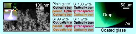
Coating by liquid flame spray
FLTR: Coating by liquid flame spray; surface SEM ; letters on paper below liquid repellent coating; confocal microscopy image of water drop resting on coating on glass. (© Wiley)
Potential applications of surfaces that are super liquid-repellent range from protective and self-cleaning textiles, goggles and windows for medical devices and gas exchange membranes. Applications of liquid-repellent coatings depend not only on their wetting properties, but also on their transparency, robustness, and fabrication cost and speed. Besides of being super-repellent against liquids, this new coating shows high transparency and withstands impacting high-velocity oil and water drops.
These extraordinary properties are based on a specific structure of the coating composed of nanometer-sized silicon dioxide–titanium dioxide particles. The method can be scaled up to coat large surface areas. Liquid flame spray is already used in industry to color glass and produce optical fibers. As the exposure time of the substrate to the flame is extremely short, even highly flammable materials like paper and wood can be coated.
The researchers have combined this fast and scalable processing method with the extraordinary liquid-repellent properties. They also discussed the criteria the coating needs to fulfill to achieve the superior liquid repellency. They described in detail how they managed to tune the coating morphology to meet these criteria. Their strategy can be widely applied to produce coatings composed of different materials because liquid flame spray can be used to synthesize a broad range of oxides, metal nanoparticles, and their mixtures.
Source: Max Planck Institute for Polymer Research