Superacidul este un medicament bun pentru semiconductorii subțiri(Superacids are good medicine for super thin semiconductors)

Tratarea semiconductorului 2-D cu un superacid vindecă defectele structurale și îmbunătățește performanța electronică a materialului. au implementat un tratament superacid pentru defectele de vindecare în filmele subțiri MoS 2 . Aceștia au arătat că acest tratament chimic simplu este compatibil cu fabricarea dispozitivelor electronice ( Applied Physics Letters , „Proprietățile materialelor și ale dispozitivelor disulfurului de molibden monolayer tratat cu superacid” )

Posted: Apr 10, 2018

Superacids are good medicine for super thin semiconductors

(Nanowerk News) Designing wearable sensors or other devices demands robust, flexible electronics. Extremely thin films, just one atom thick, such as molybdenum disulfide (MoS2), hold promise. Large-area synthesis of these materials is required for their commercialization. But today’s thin films are plagued by structural defects. These defects degrade device performance.

Scientists at New York University and the Center for Functional Nanomaterials have implemented a superacid treatment for healing defects in thin MoS2 films. They showed that this straightforward chemical treatment is compatible with electronic device fabrication (Applied Physics Letters, „Material and device properties of superacid-treated monolayer molybdenum disulfide”). Also, the process boosts device performance by reducing the density of defects in the material.
2-D molybdenum disulfide semiconductor
(Top) Illustration shows a 2-D molybdenum disulfide (MoS2) semiconductor with structural defects such as missing surface atoms. (Bottom) Treating the 2-D semiconductor with a superacid heals structural defects and improves the electronic performance of the material. (Image: Brookhaven National Laboratory)
Wearable computers are an emerging trend. To capitalize on this trend, industry needs mechanically flexible devices. Thin films can enable power-efficient and high-speed devices. This work is a vital step toward realizing wearable devices.
The atomically thin nature of layered 2-D semiconductors gives rise to a gamut of unique physical properties, which often do not exist in traditional bulk semiconductors such as silicon. These physical properties can enable a new family of devices, from sensors to logic switches, that have superior performance compared with their conventional counterparts.
Producing defect-free 2-D materials on a large scale underpins the translation of basic scientific studies into real products. However, synthetic 2-D materials are plagued with large numbers of defects that suppress many of their useful properties.
In the ongoing quest to achieve large defect-free 2-D semiconductors, scientists at New York University have shown that a superacid treatment boosts the performance of devices made from monolayer 2-D MoS2. In collaboration with scientists at the Center for Functional Nanomaterials, they used an advanced material characterization technique, called Nano-Auger, to study the structure of 2-D MoS2 on the atomic scale. They discovered that the superacid treatment is mostly effective in healing defects in the regions of MoS2 that have missing sulfur atoms.
These findings are important steps toward realizing high-performance devices from synthetic 2-D semiconductors.
Source: U.S. Department of Energy, Office of Science

Știința tubulară îmbunătățește celulele solare polimerice(Tubular science improves polymer solar cells)

Centrul pentru Materiale Nanoscale și echipa de la Universitatea Stony Brook au demonstrat că adăugarea unei componente treilea polimer la amestecul binar de materiale organice cu celule solare duce la o nanostructură coloană autostopică asamblată. Acest lucru a îmbunătățit mobilitatea încărcării și performanța fotovoltaică în dispozitivele cu grosimi de strat mai mari de 300 nanometri – mai mult de trei ori mai groase decât cele tipice.

Posted: Apr 10, 2018

Tubular science improves polymer solar cells

(Nanowerk News) A popular polymer-based solar cell could produce more energy if the electronic charges can move efficiently through the cell’s components. A novel three-component mixture allows conductive solar cell materials to self-align into columns (Nanoscale, „A new strategy to engineer polymer bulk heterojunction solar cells with thick active layers via self-assembly of tertiary columnar phase”).

The alignment improves the efficiency. This, in turn, allows the solar cells to be fabricated more than three times thicker without degrading the high performance. The greater depth makes the process more compatible with conventional industrial coating processes.
Illustration of a three-component blend polymer-based solar cell
Illustration of a three-component blend polymer-based solar cell: (1) polymer plates (pink), (2) fullerene (a.k.a. buckyballs, grey spheres) active components, and (3) a columnar polymer (dark grey columns) that promotes self-assembly of efficient, columnar charge collection pathways (green arrows). (Image: Center for Functional Nanomaterials at Brookhaven National Laboratory)
Reliable manufacturing. High performance. The internal architectures formed by this new blend of three components has potential to make these materials more amenable to reliable manufacturing. The devices can be made at greater thicknesses. These depths are better suited for conventional industrial coating processes but still allow the cell to maintain its high performance.
Low-cost, large-area scalability by solution processing is an important advantage of organic polymer solar cells. Typical organic solar cells, however, require active layer thicknesses of less than 100 nanometers (about 0.000004 inches) for optimal performance, due to the limitations of polymer semiconductor charge carrier mobility. This presents a significant challenge for solution-based manufacturing—large-area coating technologies (for example, roll-to-roll or slot-die coatings) are unable to provide reliable films at such thin dimensions.
The Center for Nanoscale Materials and Stony Brook University team demonstrated that adding a third polymer component to the binary blend of organic solar cell materials leads to a self-assembled columnar nanostructure. This enhanced the charge mobility and photovoltaic performance in devices with layer thicknesses of more than 300 nanometers—more than three times thicker than typical.
Detailed experimental studies and simulations reveal that interfacial tension between the polymeric components is crucial for obtaining the self-assembled columnar nanoarchitecture that provides efficient charge extraction pathways.
Practically, this ternary blend organic solar cell architecture has potential to enable reliable large-area manufacturing because the devices can be made thicker for conventional industrial coating processes.
Source: U.S. Department of Energy, Office of Science

Aliajul nanostructurat cu oxigen(Nanostructured alloying with oxygen)

pentru a produce materiale nanostructurate cu compoziții personalizate și fără efortul de precasting. Acestea permit producerea de noi materiale nanocristaline metalice prin aliaje mecanice ale elementelor nemiscibile. Contaminarea cu oxizi în timpul procesării acestor pulberi încă împiedică această metodă să fie aplicată în industrie în mod cuprinzător.

Posted: Apr 09, 2018

Nanostructured alloying with oxygen

(Nanowerk News) Severe plastic deformation and powder processing techniques are used to produce nanostructured materials with tailor-made compositions and without the effort of precasting. They allow the production of novel metallic nanocrystalline materials by mechanically alloying immiscible elements. Oxide contamination during the processing of these powders still hinders this method to be applied in industry comprehensively.

Meanwhile it is also known that oxygen could be used beneficially to influence morphology, mechanical properties and thermal stability of nanostructured alloys. Up to now this possibility is still not used as it is unclear how oxide behaves during annealing.
Scientists from the Max-Planck-Institut für Eisenforschung (MPIE), the Austrian Erich Schmid Institute of Material Science, the Universities Leoben and Graz (Austria) and the Chinese Hubei University analysed in-situ copper-iron alloys during annealing to find out when and how oxide is formed and how it can be used to strengthen nanocrystalline materials. They published their latest findings in Nature Communications („In situ atomic-scale observation of oxidation and decomposition processes in nanocrystalline alloys”).
Dr. Jazmin Duarte
Dr. Jazmin Duarte did atom probe tomography measurements to characterize the sample and see the oxide distribution. (Image: Max-Planck-Institut für Eisenforschung)
“By combining different experimental methods and density-functional theory calculations, we studied the thermal behaviour of oxygen in nanocrystalline copper-iron alloys which were fabricated under severe deformation and high pressure. During the heating process but still at very low temperatures, oxidation starts, leading to the formation of nanosized copper and iron oxides inside grains. Later in the heating process the metastable copper-iron solid solution decomposes into iron- and copper-rich phases,” explains Dr. Jazmin Duarte, senior researcher in the department “Structure and Nano-/Micromechanics of Materials”.
The copper and iron oxides and iron precipitates grow with annealing temperature, till they reach approximately 10 nanometres. Both oxide distributions are almost identical, which means that oxygen diffuses to one specific area during heating, simultaneously triggering the nucleation processes of oxides.
“For the first time a direct observation of oxide formation in single-phase copper-iron alloys was possible. We also did several comparison studies and ex situ analyses to make sure that neither the electron beam of the transmission electron microscope nor the sample size have an influence on the oxidation and precipitation processes. This new insights give us the possibility of manipulating mechanical properties by including oxygen into nanocrystalline alloys. Oxygen which was formerly seen as contamination to be avoided, can now be used as an ingredient to form advanced, nanostructured alloys,” explains Prof. Gerhard Dehm, director at the MPIE.
The scientists are now further studying the mechanisms by which oxygen can be introduced into the alloys and how the microstructure and consequently the mechanical behaviour are affected by an increased content of dissolved oxygen. Such tailor-made microstructures could be then used to engineer oxide strengthened nanocrystalline materials for specific applications.
Source: Max-Planck-Institut für Eisenforschung

Aurul modifică fotoluminescența punctelor cuantice de siliciu(Gold changes the photoluminescence of silicon quantum dots)

Biosenzorii bazați pe puncte cuantice de siliciu pot fi utilizați ca un instrument de diagnosticare precoce pentru diferite afecțiuni, în timp ce nanocristalele de siliciu prezintă un mare potențial pentru dezvoltarea dispozitivelor de emisie de lumină bazate pe siliciu și producerea celulelor solare foarte eficiente.

Posted: Apr 09, 2018

Gold changes the photoluminescence of silicon quantum dots

(Nanowerk News) A group of scientists from Russia and Sweden have demonstrated that applying gold stripes to a sample with silicon quantum dots modifies the dots’ properties. Their results of the study were published in Scientific Reports („Plasmon induced modification of silicon nanocrystals photoluminescence in presence of gold nanostripes”).

applying gold stripes to a sample with silicon quantum dots modifies the dots’ properties
(Image: Sergey Dyakov, Nikolay Gippius) (click on image to enlarge)
Silicon quantum dots have a wealth of potential applications in cell biology and medicine thanks to their selective cell penetration capability and luminescence. Biosensors based on silicon quantum dots can be used as an early diagnosis tool for various diseases, while silicon nanocrystals hold great potential for developing silicon-based light-emitting devices and producing highly efficient solar cells.
Scientists from the theoretical nanophotonics team led by Skoltech Professor Nikolay Gippius jointly with researchers from Moscow State University and the Royal Institute of Technology (KTH) in Stockholm demonstrated, first theoretically and then experimentally, that gold nanostripes are capable of changing the extinction and photoluminescence spectra of silicon nanocrystals. They established that the nanostripe width also affects the optical properties of the quantum dots.
The researchers’ findings are of particular value for practical applications of silicon nanocrystals, as they provide scientists with a novel tool for controlling the quantum dots’ properties.
Interestingly, the use of silicon quantum dots in photocells would significantly reduce technical losses in the solar power industry and help to avoid using arsenic, lead and other toxicants in solar cells production.
“Derived from the interaction between a sample of silicon quantum dots and gold nanostripes is a quasiparticle called the ‘waveguide plasmon polariton.’ This leads to a change in the optical properties of silicon nanocrystals. If we wish to use them in solar batteries or light emitters, we should have a metal electrode and know how to control the extinction and emission spectra.
Gold nanostripes are a solution to both issues,” said Sergey Dyakov, the main author of the study and a Skoltech researcher.
Source: Skolkovo Institute of Science and Technology

Celuloza fotonica iridescenta, imitand culoarea structurala a insectelor, cu aplicatii optice(Iridescent photonic cellulose, mimicking the structural color of insects, with optical applications)

creează pentru prima dată cristale fotonice și structuri plasmonice a unui derivat de celuloză prin nanostructurarea sa cu tehnica de litografie moale. Prin nanostructarea periodică a filmului de celuloză, acesta nu mai este transparent și începe să reflecte culori intense, în funcție de modelul cu care a fost turnat.

Posted: Apr 09, 2018

Iridescent photonic cellulose, mimicking the structural color of insects, with optical applications

(Nanowerk News) The bright colors of some butterflies, beetles or birds are not due to the presence of pigments that selectively absorb light, but due to the so-called structural coloration. Structural coloration occurs on surfaces with a nanostructure with dimensions similar to those of the wavelength of the incident light (typically below the micron). These ordered nanostructures are known as photonic crystals. There is a great interest in providing cellulose, the most abundant polymer in earth, biocompatible and biogradable, with these structures, which can offer new optical and electric functionalities.

The study published today in Nature Photonics („Hydroxypropyl cellulose photonic architectures by soft nanoimprinting lithography”), led by Dr. Agustín Mihi of the Institute of Materials Science of Barcelona (ICMAB-CSIC), creates for the first time photonic crystals and plasmonic structures of a cellulose derivative through its nanostructuring with the soft lithography technique. By periodically nanostructuring the cellulose film, it is no longer transparent and begins to reflect intense colors, depending on the pattern with which it has been molded.
The colors obtained do not depend on pigments but on nanostructures that interact differently with the incident light, therefore presenting different colors
The colors obtained do not depend on pigments but on nanostructures that interact differently with the incident light, therefore presenting different colors. (Image: ICMAB)
With this new, fully scalable and low cost technique, alternative to the traditional self-assembly of cellulose nanocrystals, a high quality and reproducible nanostructure is created on this polymer in a very short time, and achieving a wide range of iridescent colors, only depending on the size and morphology of the created structures.
These photonic crystals can be nanoimprinted on different substrates to provide photonic properties on surfaces that do not present this property, such as paper, demonstrating the potential of this technology as photonic ink, for applications in anti-counterfeiting technology, packaging, decorative paper, labels or sensors, among others.
When these structures are covered with a thin metal layer, they acquire plasmonic properties while maintaining their flexibility, achieving brighter colors. Furthermore, depending on the type of cellulose derivative used, its degree of biodegradability and solubility in water can be tuned. These plasmonic structures can be used as disposable sensors for Raman emission or to increase the light emitted by a dye.
Photonic crystals and plasmonic architectures are used in optics for their ability to manipulate light. In this work, these interesting optical properties are obtained in a biocompatible and biodegradable material, which can open up new fields of application. The study has been funded by the European Research Council (ERC Sarting Grant) through the the ENLIGHTMENT project, and by the Severo Ochoa project of the ICMAB.

Source: ICMAB

Cercetările solide determină fizicienii să propună o nouă stare de materie(Solid research leads physicists to propose new state of matter)

propunerea unui nou tip de materie care este atât superfluid cât și quasicrystal.Un supersolid este un lichid care curge fără frecare ale cărui atomi sunt de asemenea aranjate într-un mod periodic, la fel cum sunt într-un solid de cristal”, a spus el. „Aceste două stări, care se exclud reciproc în viața noastră de zi cu zi, pot exista în același timp în același material fizic în lumea cuantică”.

Posted: Apr 09, 2018

Solid research leads physicists to propose new state of matter

(Nanowerk News) The term „superfluid quasicrystal” sounds like something a comic-book villain might use to carry out his dastardly plans.

In reality, it’s a new form of matter proposed by theoretical physicists at The University of Texas at Dallas in a recent study published in the journal Physical Review Letters („Superfluid-Quasicrystal in a Bose-Einstein Condensate”). Their study also describes a „recipe” for making the exotic materials in the lab.
From left: The research team includes doctoral student Junpeng Hou; Dr. Kuei Sun, senior lecturer; Dr. Chuanwei Zhang, professor of physics; and Dr. Haiping Hu, a postdoctoral research associate
From left: The research team includes doctoral student Junpeng Hou; Dr. Kuei Sun, senior lecturer; Dr. Chuanwei Zhang, professor of physics; and Dr. Haiping Hu, a postdoctoral research associate.
Most people are familiar with the three fundamental states of matter: solid, liquid and gas. There are actually several more, including plasma, which is found inside the sun and other stars, and Bose-Einstein condensates, which are very dense and exist only at the most extreme cold temperatures.
A superfluid is an exotic state of matter with unusual properties. It has zero viscosity, which means it can flow across a surface and not slow down – or lose any energy – due to friction with the surface. Superfluids, such as liquid helium, must be cooled to extremely low temperatures for such properties to emerge.
„If your morning coffee was a superfluid, and you stirred it with a spoon, you could remove the spoon and the coffee would never stop moving,” said Dr. Chuanwei Zhang, professor of physics in the School of Natural Sciences and Mathematics and corresponding author of the study. „Regular fluids will eventually stop due to friction with the cup.”

Both a Superfluid and a Quasicrystal

About 50 years ago, researchers proposed a new type of matter that combined the properties of a superfluid with those of a solid crystal. Dubbed a supersolid, it’s only been in the past couple of years that scientists have been able to produce that unusual material in the lab.
„In physics, we have a very strict definition of what a fluid is and what a solid is,” Zhang said. „Liquid water cannot behave as a solid, and vice versa. They can be mixed together, for example in a glass of ice water, but they are still separate forms of matter.”
In the world of quantum physics, which describes how matter behaves at the level of atoms and individual particles, this is not always true, Zhang said.
„A supersolid is a fluid flowing without friction whose atoms are also arranged in a periodic way, just as they are in a crystal solid,” he said. „These two states, which are mutually exclusive in our everyday life, can exist at the same time in the same physical material in the quantum world.”
In their new study, Zhang and his colleagues suggest the next logical step – proposing a new type of matter that is both a superfluid and a quasicrystal.
A crystal, like table salt, has atoms that are arranged in a highly ordered, periodic pattern that is unchanged when you rotate or repeat it, Zhang said. A checkerboard can be thought of as a two-dimensional crystal. Quasicrystals, on the other hand, are materials whose atoms are ordered and have structure like in a crystal, but their arrangement is not periodic – it does not repeat.
„We asked the question, can you have a new quantum matter state that is both a quasicrystal and a superfluid?” Zhang said.
The answer is yes, at least from physical principles, Zhang said.
The material Zhang and his colleagues propose should flow without friction while also exhibiting a nonperiodic, quasicrystal structure.
„This is a theory at the moment, but in this paper we suggest an experimental setup similar to the experiment that produced the first supersolids,” Zhang said. „The good news is, we shouldn’t have to invent any new technology to actually make this material. It basically involves shooting lasers at a Bose-Einstein condensate.”
Junpeng Hou, the lead author of the study and a physics PhD student at UT Dallas, said producing the material might still be challenging.
„It can take several years for new supersolids to become experimentally realized,” Hou said. „But I believe our system would not take that long, maybe one or two years.”
Source: University of Texas at Dallas

Un nou mod de a substitui materialele atomice(A new way to atomically thin materials)

Materialele bidimensionale, formate din straturi extrem de subți, cu grosime de câteva atomi, au proprietăți unice care sunt complet diferite de versiunile normale tridimensionale. Un exemplu proeminent al acestui lucru este grafenul, care este format din straturi unice de atomi de carbon. În 2011, a fost sintetizată o nouă clasă de materiale bidimensionale la Universitatea Drexel din Philadelphia (Pennsylvania, SUA).
Cunoscute ca MXenes, materialele sunt fabricate din carburi metalice de tranziție și nitruri, unde M reprezintă un metal de tranziție, cum ar fi titan, vanadiu sau molibden, X poate fi carbon și / sau azot și sunt disponibile multe compoziții (circa 30 au fost deja demonstrate experimental și se așteaptă zeci de alte). Un astfel de MXene este carbură de titan, Ti 3 C 2 .

Posted: Apr 09, 2018

A new way to atomically thin materials

(Nanowerk News) Metallic conductivity and hydrophilicity of MXenes have established them as electrodes in rechargeable batteries and supercapacitors, as well as other applications, including photothermal cancer therapy, electromagnetic shielding, water purification and gas sensing.

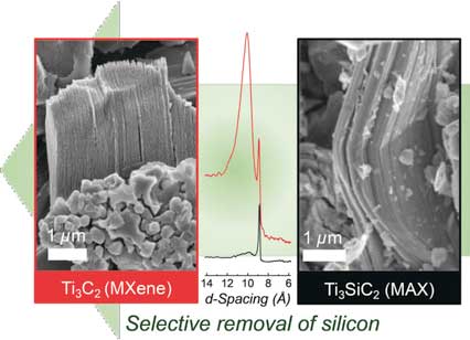
In the journal Angewandte Chemie („Selective Etching of Silicon from Ti3SiC2 (MAX) To Obtain 2D Titanium Carbide (MXene)”), researchers have now introduced a new production method. Instead of using conventional, yet more expensive, titanium aluminum carbide, they selectively etch silicon out of titanium silicon carbide, a cheaper and more common precursor, to synthesize titanium carbide.
Silicon secedes: titanium carbide flakes obtained by selective etching of titanium silicon carbide
A new way to atomically thin materials – Silicon secedes: titanium carbide flakes obtained by selective etching of titanium silicon carbide. (© Wiley-VCH)
Two-dimensional materials, consisting of extremely thin layers that are a few atoms thick, have unique properties that are completely different than the normal three-dimensional versions. A prominent example of this is graphene, which is made of single layers of carbon atoms. In 2011, a new class of two-dimensional materials was synthesized at Drexel University in Philadelphia (Pennsylvania, USA).
Known as MXenes, the materials are made of transition metal carbides and nitrides, where the M stands for a transition metal, such as titanium, vanadium, or molybdenum, X can be carbon and/or nitrogen, and many compositions are available (about 30 have already been experimentally demonstrated and dozens more are expected). One such MXene is titanium carbide, Ti3C2.
Obtaining the desired MXene usually involves a roundabout process: Layered carbides and nitrides, known as MAX phases, are selectively etched with hydrofluoric acid to remove the layers of the “A” element, which is a group 13 or 14 element such as aluminum, silicon, or germanium. In this way, titanium carbide can be obtained by etching the aluminum out of titanium aluminum carbide (Ti3AlC2). However, this starting material is expensive, and the production is complex.
In contrast, the silicon analog, titanium silicon carbide (Ti3SiC2), is commercially available and less expensive. Ti3SiC2 was the first MAX phase Drexel researchers tried to selectively etch in 2011, but synthesis failed using hydrofluoric acid alone because the silicon atoms are strongly bound to the adjacent transition metal atoms.
A team led by Yury Gogotsi at Drexel University has now developed a successful variation of this process. By adding an oxidizing agent, the researchers could weaken the silicon bonds and oxidize silicon. Using mixtures of hydrofluoric acid and an oxidizing agent like nitric acid, hydrogen peroxide, or potassium permanganate, the team produced titanium carbide MXene by selectively removing silicon out of Ti3SiC2.
The etching process leaves behind stacks of titanium carbide, which can be delaminated to make flakes, which are approximately 1 nanometer in thickness. The researchers used this method to make flexible, electrically conducting titanium carbide films on a relatively large scale.
This new method could make the production of MXenes easier, and open pathways to the production of new MXenes and related two-dimensional materials from silicon-containing precursors, expanding the family of 2D nanosheets available to scientists and engineers.
Source: Wiley

Convertirea energiei solare de înaltă eficiență este permisă de un material compozit nou(High efficiency solar power conversion allowed by a novel composite material)

Materialul compozit conduce la o eficiență a conversiei de putere de până la 4,2%, valoare care este o valoare record pentru această clasă de materiale.n urma unui concept original al dispozitivului, domnul Joyprokash Chakrabartty, cercetătorii au dezvoltat acest nou material compozit subțire, care combină două faze cristaline diferite, care conțin elemente atomice bismut, mangan și oxigen.

Posted: Apr 09, 2018

High efficiency solar power conversion allowed by a novel composite material

(Nanowerk News) A composite thin film made of two different inorganic oxide materials significantly improves the performance of solar cells, as recently demonstrated by a joint team of researchers led by Professor Federico Rosei at the Institut national de la recherche scientifique (INRS), and Dr. Riad Nechache from École de technologie supérieure (ÉTS), both in the Montreal Area (Canada).

Following an original device concept, Mr. Joyprokash Chakrabartty, the researchers have developed this new composite thin film material which combines two different crystal phases comprising the atomic elements bismuth, manganese, and oxygen.
The combination of phases with two different compositions optimizes this material’s ability to absorb solar radiation and transform it into electricity. The results are highly promising for the development of future solar technologies, and also potentially useful in other optoelectronic devices.
The results of this research are discussed in an article published in Nature Photonics („Improved photovoltaic performance from inorganic perovskite oxide thin films with mixed crystal phases”) by researchers and lead author Mr. Joyprokash Chakrabartty.
The key discovery consists in the observation that the composite thin film—barely 110 nanometres thick—absorbs a broader portion of the solar spectrum compared to the wavelengths absorbed in the thin films made of the two individual materials. The interfaces between the two different phases within the composite film play a crucial role in converting more sunlight into electricity. This is a surprising, novel phenomenon in the field of inorganic perovskite oxide-based solar cells.
The composite material leads to a power conversion efficiency of up to 4.2%, which is a record value for this class of materials.
Source: INRS

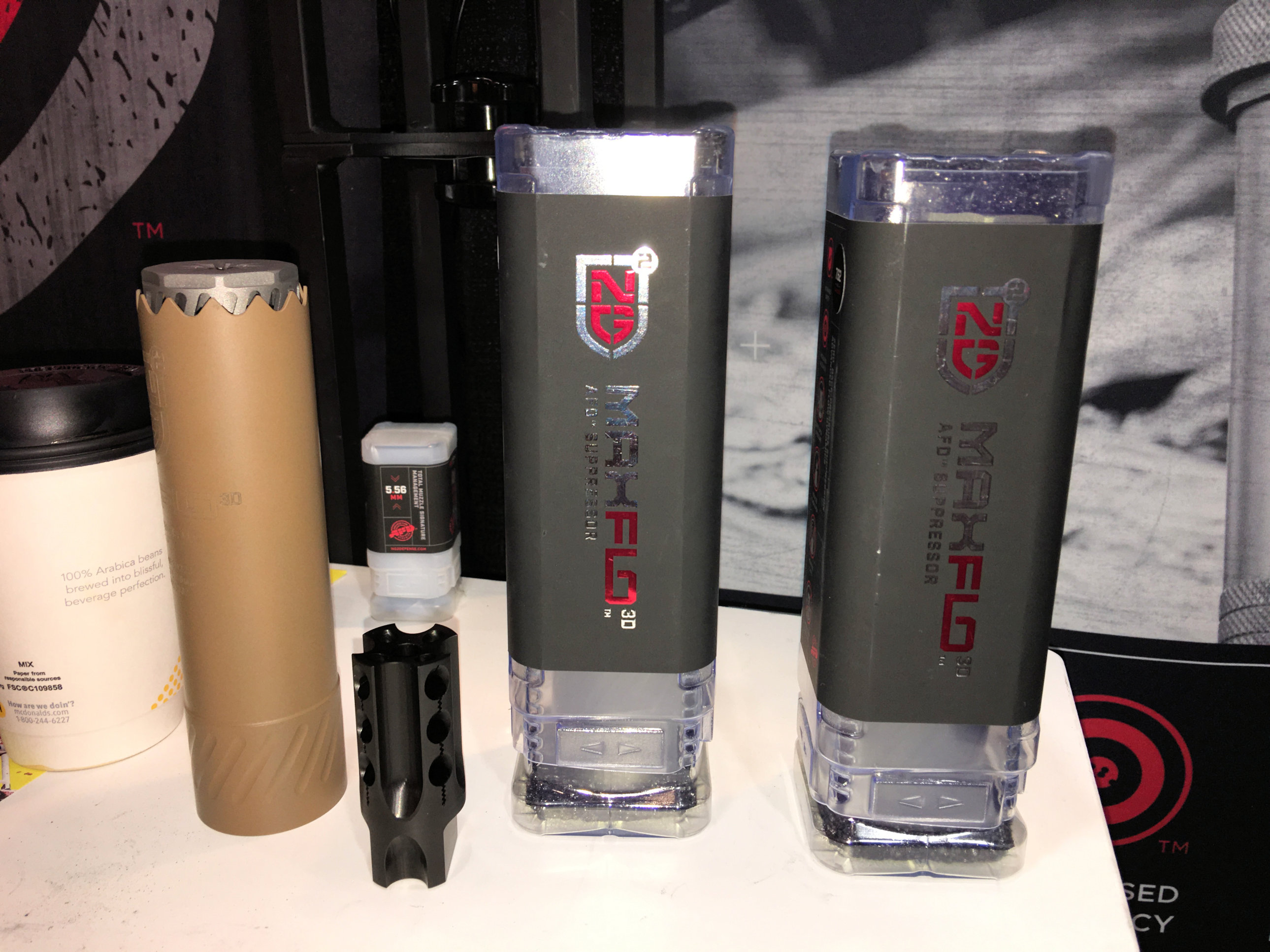
NG2 Defense MAXFLO 3D AFD Supresor de zero-supresiune cu randament maxim: Auto Pop it on and go!(NG2 Defense MAXFLO 3D AFD Full-Auto-Rated Zero-Back-Pressure Suppressor: Just Pop it on and Go)

dar principalele puncte sunt că NG2 are cutii cu presiune zero, cu capacitate maximă, care pot fi aruncate rapid pe pușca, carabina sau SBR (pușca cu șuruburi scurte) și apoi s-au retras din nou.

DR nu este, de fapt, străin de supresoare cu presiune zero. Am acoperit suporterii OSS pentru o vreme, chiar și atunci când erau cunoscuți sub numele de Bravo 18. Ultimele cutii Helix QD OSS arată foarte bine, dar din nou, la fel și cutii NG2. Cine sunt superior? DR nu știe încă. Ar trebui să vedem cum se efectuează amândurora în testarea militară în condiții de luptă nefavorabile la numărătoare rotundă atât în ​​focul complet cât și semiautomat.

NG2 Defense MAXFLO 3D AFD Full-Auto-Rated Zero-Back-Pressure Suppressor: Just Pop it on and Go! (Video!)

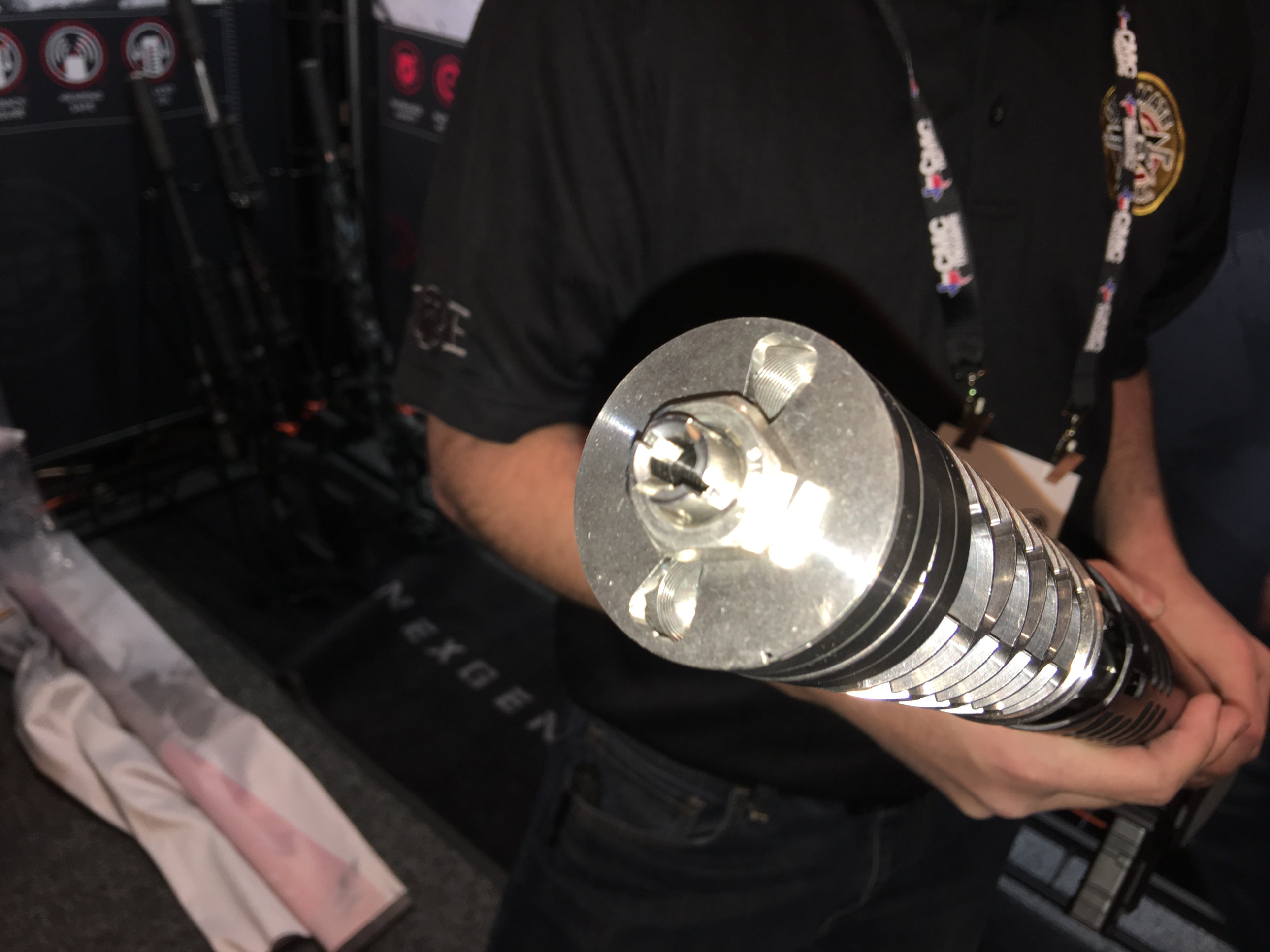
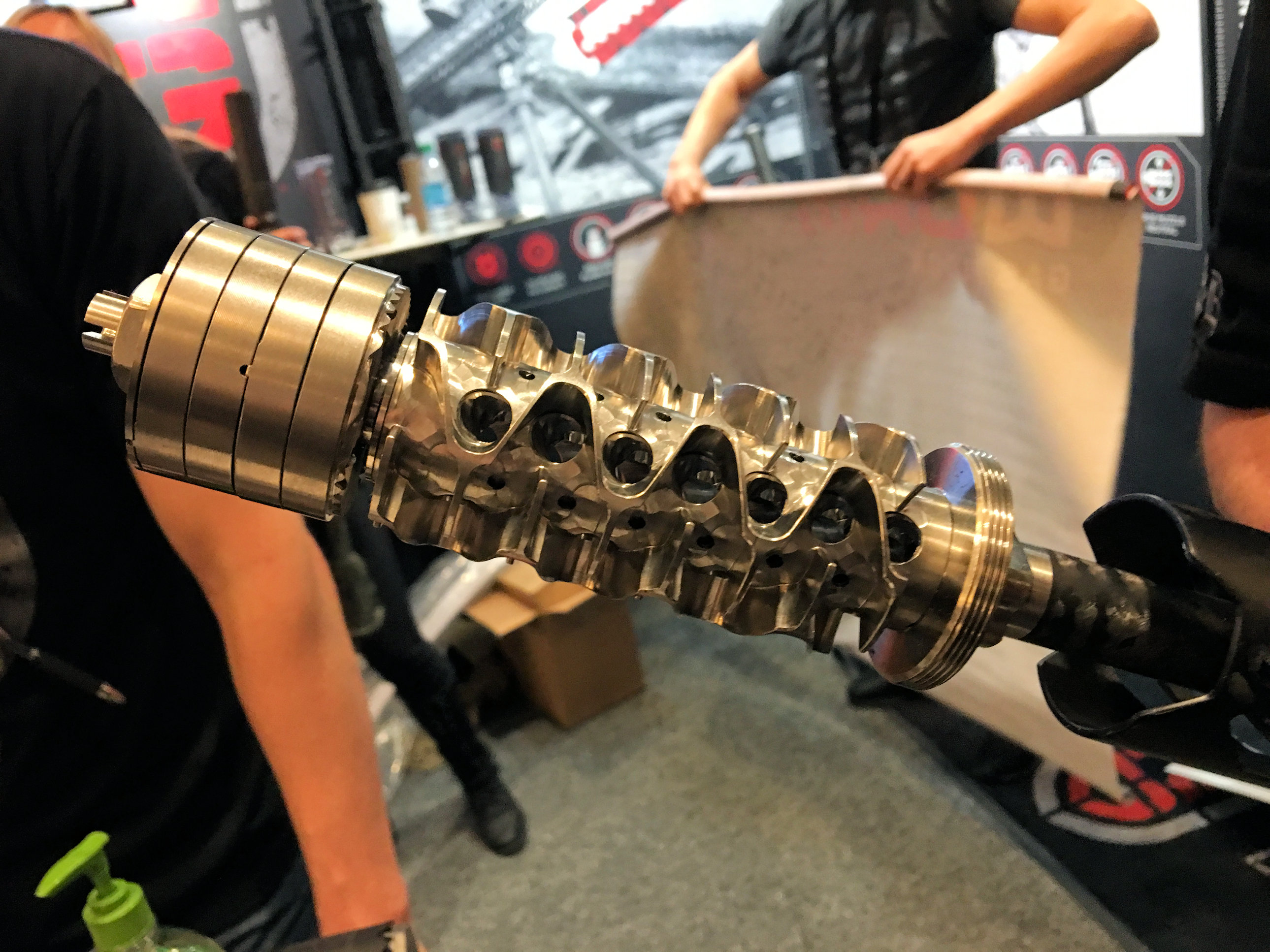
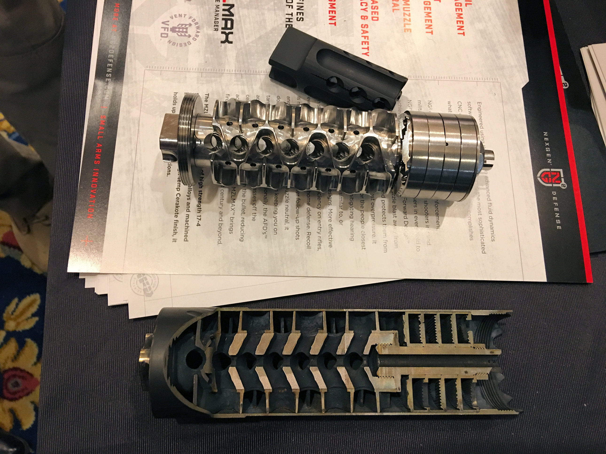
As DefenseReview (DR) alluded to in our previous piece on the Joe Firearms AJAK Enhanced Combat/Tactical AK’s, there’s a new zero-back-pressure-suppressor game in town called NexGen2 Defense, or NG2 Defense for short, and they’re creating a lot of interest and excitement with their NG2 MAXFLO 3D AFD (Advanced Flow Dynamics rifle cans (silencers/sound suppressors) in both 5.56MM NATO (5.56x45mm NATO)/.223 Rem. and 7.62mm NATO (7.62x51mm NATO)/.308 Win., and DR got chance to see how the technology works at SHOT Show 2018. As you can see in DR’s video below, company founder/designer/inventor Ernie Bray was kind enough to show us a cutaway version of one of his suppressors, and explain its tech to us in considerable depth–but the main points are that NG2 has full-auto-rated zero-back-pressure cans that can be quickly popped onto your rifle, carbine or SBR (Short Barreled Rifle), and then popped right back off again. Pretty cool.

DR’s actually no stranger to zero-back-pressure suppressors. We’ve been covering OSS Suppressors for awhile, even back when they were known as Bravo 18. The latest Helix QD OSS cans look pretty great, but then again, so do the NG2 cans. Who’s are superior? DR doesn’t know yet. We’d have to see how both perform in military testing in adverse combat-type conditions at high-round-count in both full-auto and semi-auto fire. In the meantime, Defense Review will just let Mr. Bray take our readers through the NG2 MAXFLO 3D AFD Suppression tech and capabilities in our video below.


Company Contact Info:

NexGen2 Defense (NG2) Headquarters
218 West 12650 South
Draper, Utah 84020
Phone: 801.692.7091
Email: [email protected]
Website: https://www.ng2defense.com

NG2 Dealer Contact Info:

Phone: 801.692.7094
Email: [email protected]

Sentinel wrap: Un plasture transparent pentru detectarea pericolelor alimentare periculoase(Sentinel wrap: A transparent patch to detect dangerous food threats)

Un plasture transparent pentru detectarea pericolelor alimentare periculoase. dezvolta un plasture de testare transparent, tipărit cu molecule inofensive, care pot semnala contaminarea așa cum se întâmplă. Plasturele poate fi încorporat direct în ambalajul alimentar, unde poate monitoriza conținutul agenților patogeni nocivi precum E. coli și Salmonella.

Posted: Apr 06, 2018

Sentinel wrap: A transparent patch to detect dangerous food threats

(Nanowerk News) Is that meat still good? Are you sure? McMaster researchers have developed a test to bring certainty to the delicate but critical question of whether meat and other foods are safe to eat or need to be thrown out.

Mechanical and chemical engineers at McMaster, working closely with biochemists from across campus, have collaborated to develop a transparent test patch, printed with harmless molecules, that can signal contamination as it happens. The patch can be incorporated directly into food packaging, where it can monitor the contents for harmful pathogens such as E. coli and Salmonella.
Real-Time Monitoring of Food Contamination by Printing DNAzyme Probes on Food Packaging
The team has a transparent, durable, and flexible sensing surface that generates a fluorescence signal in the presence of a specific target bacterium. (© ACS)
The new technology, described in the research journal ACS Nano („Sentinel Wraps: Real-Time Monitoring of Food Contamination by Printing DNAzyme Probes on Food Packaging”), has the potential to replace the traditional „best before” date on food and drinks alike with a definitive indication that it’s time to chuck that roast or pour out that milk.
„In the future, if you go to a store and you want to be sure the meat you’re buying is safe at any point before you use it, you’ll have a much more reliable way than the expiration date,” says lead author Hanie Yousefi, a graduate student and research assistant in McMaster’s Faculty of Engineering.
If a pathogen is present in the food or drink inside the package, it would trigger a signal in the packaging that could be read by a smartphone or other simple device. The test itself does not affect the contents of the package.
According to the World Health Organization, foodborne pathogens result in approximately 600 million illnesses and 420,000 deaths per year. About 30 per cent of those cases involve children five years old and younger.
The researchers are naming the new material „Sentinel Wrap” in tribute to the McMaster-based Sentinel Bioactive Paper Network, an interdisciplinary research network that worked on paper-based detection systems. That network’s research ultimately gave rise to the new food-testing technology.
Chemical engineer Carlos Filipe and mechanical-biomedical engineer Tohid Didar, collaborated closely on the new detection project.
The signaling technology for the food test was developed in the McMaster labs of biochemist Yingfu Li.
„He created the key, and we have built a lock and a door to go with it,” says Filipe, who is Chair of McMaster’s Department of Chemical Engineering.
Mass producing such a patch would be fairly cheap and simple, the researchers say, as the DNA molecules that detect food pathogens can be printed onto the test material.
„A food manufacturer could easily incorporate this into its production process,” says Didar, an assistant professor of mechanical engineering and member of the McMaster Institute for Infectious Disease Research.
Getting the invention to market would need a commercial partner and regulatory approvals, the researchers say. They point out that the same technology could also be used in other applications, such as bandages to indicate if wounds are infected, or for wrapping surgical instruments to assure they are sterile.
Source: McMaster University

Lumina „relaxează” cristalul pentru a crește eficiența celulelor solare(Light ‘relaxes’ crystal to boost solar cell efficiency)

a constatat ca este cazul unui compus perovskitat ca un material eficient pentru a colecta lumina soarelui si a-l transforma in energie.Sa descoperit o iluminare constantă pentru a relaxa zăbrelele unui material asemănător perovskitei, făcând-o mai eficientă în colectarea luminii solare și transformarea acesteia în energie. Materialul stabil a fost testat pentru utilizarea celulelor solare de către oamenii de știință de la Universitatea Rice și Laboratorul Național Los Alamos.

Posted: Apr 05, 2018

Light ‘relaxes’ crystal to boost solar cell efficiency

(Nanowerk News) Some materials are like people. Let them relax in the sun for a little while and they perform a lot better.

A collaboration led by Rice University and Los Alamos National Laboratory found that to be the case with a perovskite compound touted as an efficient material to collect sunlight and convert it into energy (Science, „Light-induced lattice expansion leads to high-efficiency perovskite solar cells”).
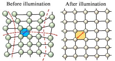
The researchers led by Aditya Mohite, a staff scientist at Los Alamos who will soon become a professor at Rice; Wanyi Nie, also a staff scientist at Los Alamos, and lead author and Rice graduate student Hsinhan (Dave) Tsai discovered that constant illumination relaxes strain in perovskite’s crystal lattice, allowing it to uniformly expand in all directions.
Constant illumination was found to relax the lattice of a perovskite-like material
Constant illumination was found to relax the lattice of a perovskite-like material, making it more efficient at collecting sunlight and converting it to energy. The stable material was tested for solar cell use by scientists at Rice University and Los Alamos National Laboratory. (Credit: Light to Energy Team/Los Alamos National Laboratory)
Expansion aligns the material’s crystal planes and cures defects in the bulk. That in turn reduces energetic barriers at the contacts, making it easier for electrons to move through the system and deliver energy to devices.
This not only improves the power conversion efficiency of the solar cell, but also does not compromise its photostability, with negligible degradation over more than 1,500 hours of operation under continuous one-sun illumination of 100 milliwatts per cubic centimeter.
The research, which appears this week in Science, represents a significant step toward stable perovskite-based solar cells for next generation solar-to-electricity and solar-to-fuel technologies, according to the researchers.
“Hybrid perovskite crystal structures have a general formula of AMX3, where A is a cation, M is a divalent metal and X is a halide,” Mohite said. “It’s a polar semiconductor with a direct band gap similar to that of gallium arsenide.
“This endows perovskites with an absorption coefficient that is nearly an order of magnitude larger than gallium arsenide (a common semiconductor in solar cells) across the entire solar spectrum,” he said. “This implies that a 300-nanometer thick film of perovskites is sufficient to absorb all the incident sunlight. By contrast, silicon is an indirect band gap material that requires 1,000 times more material to absorb the same amount of sunlight.”
Mohite said researchers have long sought efficient hybrid perovskites that are stable in sunlight and under ambient environmental conditions.
“Through this work, we demonstrated significant progress in achieving both of these objectives,” he said. “Our triple-cation-based perovskite in a cubic lattice shows excellent temperature stability at more than 100 degrees Celsius (212 degrees Fahrenheit).”
The researchers modeled and made more than 30 semiconducting, iodide-based thin films with perovskite-like structures: Crystalline cubes with atoms arranged in regular rows and columns. They measured their ability to transmit current and found that when soaked with light, the energetic barrier between the perovskite and the electrodes largely vanished as the bonds between atoms relaxed.
They were surprised to see that the barrier remained quenched for 30 minutes after the light was turned off. Because the films were kept at a constant temperature during the experiments, the researchers were also able to eliminate heat as a possible cause of the lattice expansion.
Measurements showed the “champion” hybrid perovskite device increased its power conversion efficiency from 18.5 percent to 20.5 percent. On average, all the cells had a raised efficiency above 19 percent. Mohite said perovskites used in the study were 7 percent away from the maximum possible efficiency for a single-junction solar cell.
He said the cells’ efficiency was nearly double that of all other solution-processed photovoltaic technologies and 5 percent lower than that of commercial silicon-based photovoltaics. They retained 85 percent of their peak efficiency after 800 hours of continuous operation at the maximum power point, and their current density showed no photo-induced degradation over the entire 1,500 hours.
“This work will accelerate the scientific understanding required to achieve perovskite solar cells that are stable,” Mohite said. “It also opens new directions for discovering phases and emergent behaviors that arise from the dynamical structural nature, or softness, of the perovskite lattice.”
The lead researchers indicated the study goes beyond photovoltaics as it connects, for the first time, light-triggered structural dynamics with fundamental electronic transport processes. They anticipate it will lead to technologies that exploit light, force or other external triggers to tailor the properties of perovskite-based materials.
Source: Rice University