Lasere integrate pe diferite suprafețe (Integrated lasers on different surfaces)

Legarea a fost apoi finalizată la temperaturi relativ scăzute de aproximativ 220 grade Celsius, permițând stratului ultrasonic de oxid de siliciu să efectueze căldură între straturi, reducând potențialul de deteriorare a materialelor, întărind legătura și evitând nevoia de produse chimice periculoase, cum ar fi Piranha soluție și acid fluorhidric, utilizat în legătură directă.
Lucrarea demonstrează un laser versatil pe chip care poate fi integrat pe orice platformă materială și ar putea conduce la noi aplicații pentru dispozitive fotonice, cum ar fi tehnologiile detectorului pe cip și modulatorul pe cip.
„Abordarea la intervale de joasă temperatură este mai simplă și mult mai sigură decât legătura directă și înseamnă că producătorii de laser nu sunt restricționați prin alegerea substratului”, spune Ng.

Posted: Sep 08, 2017

Integrated lasers on different surfaces

(Nanowerk News) Fabricating hybrid semiconductor lasers on materials other than the commonly used silicon-on-insulator (SOI) substrates has proved challenging. Now, A*STAR researchers have developed an innovative technique that can integrate the lasers on to a range of different materials (IEEE Journal of Selected Topics in Quantum Electronics, „Generic heterogeneously integrated III–V lasers-on-chip with metal-coated etched-mirror”).

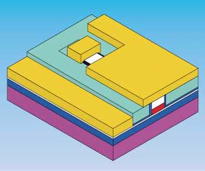
Schematic of a hybrid laser
Schematic of the hybrid laser. (Image: A*STAR Data Storage Institute)
Hybrid lasers combine the light-emitting properties of group III-V semiconductors like gallium arsenide and indium phosphide, with conventional silicon technologies, offering inexpensive photonic and microelectronic devices for application in optical telecommunication systems.
Their range of applications, however, is limited by the poor light-emitting characteristics of the silicon-on-insulator (SOI) wafers mostly used as substrates in the fabrication process. This spurred Doris Keh-Ting Ng and colleagues from the A*STAR Data Storage Institute to develop an innovative technique for bonding III-V lasers on to other substrates, be it silicon, quartz, or metal alloys.
By using an ultrathin layer of silicon oxide to bond the lasers to a silicon substrate, the researchers developed a simpler, safer and more flexible technique than direct bonding, which relies on chemical bonding between the surfaces.
“The challenge is to produce a smooth, extremely thin layer of silicon oxide on the surface of the substrate,” explains Ng. “By growing the film on the silicon substrate, but not on the III-V substrate, we greatly reduced the complexity of the process and improved the strength of the bond between the two materials.”
After first cleaning the surfaces with an organic solvent, the researchers exposed the surface to an oxygen plasma to increase its adhesive properties. They then initiated the bonding process at ambient temperature by bringing the two substrates slowly together, to reduce the air trapped between them, ensuring a much stronger bond.
The bonding was then completed at relatively low temperatures of around 220 degrees Celsius, allowing the ultrathin layer of silicon oxide to conduct heat between the layers, reducing potential damage to the materials, strengthening the bond and avoiding the need for hazardous chemicals, such as Piranha solution and hydrofluoric acid, used in direct bonding.
The work demonstrates a versatile on-chip laser that can be integrated on to any material platform and could lead to new applications for photonic devices, such as detector-on-chip and modulator-on-chip technologies.
“The low temperature interlayer approach is simpler and much safer than direct bonding, and means that laser manufacturers are not restricted by the choice of substrate,” says Ng.
Source: A*STAR

Read more: Integrated lasers on different surfaces

Cum pot fi direcționate bolile folosind nanotehnologia – și de ce este dificil( How diseases can be targeted using nanotechnology – and why it’s difficult)

anticorpul corect. Un antigen este legat de un anticorp. (Imagine: © ACS, Autor furnizat)
Aceste tipuri de nanoparticule pot funcționa bine în laborator, dar atunci când sunt utilizate în medii biologice mai complexe (cum ar fi în sânge, mai degrabă decât în ​​soluție tampon de sare), lucrurile devin rapid mai complicate.
De exemplu, atunci când nanoparticulele sunt injectate în sânge, proteinele se adsorb pe suprafața lor și acest lucru își poate schimba comportamentul complet ( Chem. , Rev. , „Corona biomoleculelor nanoparticule: lecții învățate – provocare acceptată?” ). Acest lucru se datorează faptului că această acoperire bio schimbă proprietățile importante ale particulelor, incluzând încărcarea (pozitivă, neutră sau negativă) și mărimea.Nanomaterialele administrate la o experiență de șoarece au multe niveluri diferite de complexitate biologică. Toate acestea trebuie luate în considerare la proiectarea nanomedicinei.

Posted: Sep 08, 2017

How diseases can be targeted using nanotechnology – and why it’s difficult

(Nanowerk News) Scientists are designing materials that are a thousand times smaller than the width of a hair. Known as nanomaterials or nanoparticles, some could help treat diseases.

However, the engineering of particles for biomedical applications remains challenging, particularly when moving from the test tube to biological environments.
This is an issue we discussed in a recent paper (Advanced Healthcare Materials, „Particle Targeting in Complex Biological Media”). A nanoparticle in the lab is one thing, but a nanoparticle interacting with blood, cells and tissues is another, and the behaviour of particles can change considerably when moving from one environment to another.
“Bio-nano interactions” are what govern these changes in behaviour, and this is a research area with plenty of difficulties, but also significant rewards.
layer-by-layer assembly - Using nanotechnology to prepare nanomaterials
Using nanotechnology to prepare nanomaterials. The example here is called layer-by-layer assembly. (© 2015 AAAS and 2016 ACS, Author provided)

Using nanoparticles to target diseases

Nanoparticles could help create more effective medical treatments. The aim is to improve areas ranging from drug delivery to the detection of diseases.
One of the potential benefits of nanoparticles is the possibility of developing targeted therapies, so that drugs go exactly where they are needed in the body.
For example, many highly effective chemo-therapeutics exist today, but because they do not interact only with cancer cells but with healthy ones too, many of them have side effects such as heart and bone marrow damage. This limits their efficacy and plays a big role in why treating cancer can be so difficult.

Why is targeting so hard?

But targeted drug therapies using nanoparticles also remain limited (ACS Central Science, „Does Nanomedicine Have a Delivery Problem?”). As in many other areas, what works in the laboratory can be difficult to translate into the clinic.
One example is the use of nanoparticles as “carriers” that are loaded with a drug and then accumulate at target cells (see image below).
Nanomaterials can be used to target specific cells
Nanomaterials can be used to target specific cells in the laboratory. In this image, they target/attach to the blue cells, but not to the green cells, and only when the correct antibody is used. An antigen is what an antibody binds to. (Image: © ACS, Author provided)
These types of nanoparticles can perform well in the laboratory, but when used in more complex biological environments (such as in blood rather than in salt buffer solution) things rapidly become more complicated.
For example, when nanoparticles are injected into blood, proteins adsorb onto their surface and this can completely change their behaviour (Chem. Soc. Rev., „The nanoparticle biomolecule corona: lessons learned – challenge accepted?”). This is because this bio-coating changes important properties of the particles, including charge (positive, neutral or negative) and size.

Possible solutions

New methods are being developed to evaluate nanoparticles in better ways. This includes investigative techniques that can complement cell and animal studies.
One example is microfluidic channels that can mimic blood vessels and can be used to study nanomaterial behaviour in blood capillaries.
Another option uses 3D printed tissues and organs. In one recent example, hydrogels filled with cells were printed onto a surface using a custom-built 3D printer.
The key point is to have adjustable complexity. That is, being able to adjust these methods so that we can get relevant and valuable information out of the studies. But not so complex that it becomes difficult to understand the mechanisms involved.
This is important, because a nanoparticle administered to an animal experiences several levels of biological complexity on its journey from the bloodstream to the target area (see image below). To understand fully what is happening, we need to study them all.
Nanomaterials administered to a mouse experience many different levels of biological complexity
Nanomaterials administered to a mouse experience many different levels of biological complexity. All of these need to be considered when designing nanomedicines. (Image: © ACS, Author provided)

Nanomedicines of tomorrow

The more we learn about bio-nano science – or how materials interact with biology on the nanoscale – the easier it will be to design nanoparticles that behave like we want them to.
After years of concerted efforts, a more clear picture of the mechanisms that determine how well a nanoparticle will work is emerging and the full extent of the challenge before us is starting to become clear.
It is unlikely that a single “quick fix” will be discovered.
Instead, research that manages to successfully combine ideas from different fields and researchers (JACS, „Increasing the Impact of Materials in and beyond Bio-Nano Science”) will likely lead to the development of new and improved targeted nanoparticles.
The aim is to provide new treatments for diseases that are difficult – or even impossible – to treat today.
Source: By Mattias Björnmalm, Marie Curie Research Fellow, Imperial College London and Frank Caruso, Professor and ARC Australian Laureate Fellow, University of Melbourne

Read more: How diseases can be targeted using nanotechnology – and why it’s difficult

Oamenii de știință dezvăluie noi perspective în materiale semiconductoare 2D promițătoare(Scientists unravel new insights into promising 2D semiconductor material )

au stabilit noi descoperiri cu privire la proprietatile disulfidului de molibden bidimensional (MoS 2 ), un semiconductor larg studiat al viitorului.MoS 2 – O alternativă la grafen
MoS 2 este un material semiconductor care prezintă proprietăți electronice și optice dorite pentru dezvoltarea și îmbunătățirea tranzistorilor, fotodetectoarelor și celulelor solare.structură similară cu MoS 2 .
„MoS 2 se încadrează într-un grup de materiale cunoscute sub numele de dihalcogenidele metalice de tranziție bidimensionale (2D-TMD) care prezintă un mare interes pentru cercetare din cauza potențialelor aplicații industriale. Noile cunoștințe din studiile noastre ne vor ajuta să deblocăm posibilitățile Aplicații bazate pe 2D-TMD, cum ar fi fabricarea de tranzistoare cu efect de câmp 2D-TMD „, a declarat Asst Prof Rusydi.
Folosind rezultatele acestor studii, cercetătorii vor aplica studii similare celorlalte 2D-TMD-uri și vor explora diferite posibilități de generare de proprietăți noi și valoroase în 2D-TMD care nu există în natură.

Posted: Sep 08, 2017

Scientists unravel new insights into promising 2D semiconductor material

(Nanowerk News) Researchers from the National University of Singapore (NUS) have established new findings on the properties of two-dimensional molybdenum disulfide (MoS2), a widely studied semiconductor of the future.

In two separate studies led by Professor Andrew Wee and Assistant Professor Andrivo Rusydi from the Department of Physics at the NUS Faculty of Science, the researchers uncovered the role of oxygen in MoS2, and a novel technique to create multiple tunable, inverted optical band gaps in the material. These novel insights deepen the understanding of the intrinsic properties of MoS2 which could potentially transform its applications in the semiconductor industry.
The studies were published in prestigious scientific journals Physical Review Letters and Nature Communications respectively.

MoS2 – An alternative to graphene

MoS2 is a semiconductor-like material that exhibits desirable electronic and optical properties for the development and enhancement of transistors, photodetectors and solar cells.
Prof Wee explained, „MoS2 holds great industrial importance. With an atomically thin two-dimensional structure and the presence of a 1.8eV energy band gap, MoS2 is a semiconductor that can offer broader applications than graphene which lacks a band gap.”

Presence of oxygen alters the electronic and optical properties of MoS2

In the first study published in Physical Review Letters on 16 August 2017 („Oxygen Passivation Mediated Tunability of Trion and Excitons in MoS2„), NUS researchers conducted an in-depth analysis which revealed that the energy storage capacity or dielectric function of MoS2 can be altered using oxygen.
The team observed that MoS2 displayed a higher dielectric function when exposed to oxygen. This new knowledge shed light on how adsorption and desorption of oxygen by MoS2 can be employed to modify its electronic and optical properties to suit different applications. The study also highlights the need for adequate consideration of extrinsic factors that may affect the properties of the material in future research.
The first author of this paper is Dr Pranjal Kumar Gogoi from the Department of Physics at NUS Faculty of Science.

MoS2 can possess two tunable optical band gaps

In the second study published in Nature Communications on 7 September 2017 („Tunable inverted gap in monolayer quasi-metallic MoS2 induced by strong charge-lattice coupling”), the team of NUS researchers discovered that as opposed to conventional semiconductors which typically have only one optical band gap, electron doping of MoS2 on gold can create two unusual optical band gaps in the material. In addition, the two optical bandgaps in MoS2 are tunable via a simple, straight forward annealing process.
The research team also identified that the tunable optical band gaps are induced by strong-charge lattice coupling as a result of the electron doping.
The first author of this second paper is Dr Xinmao Yin from the Department of Physics at NUS Faculty of Science.
The research findings from the two studies lend insights to other materials that possess similar structure with MoS2.
„MoS2 falls under a group of material known as the two-dimensional transitional metal dihalcogenides (2D-TMDs) which are of great research interest because of their potential industrial applications. The new knowledge from our studies will assist us in unlocking the possibilities of 2D-TMD-based applications such as the fabrication of 2D-TMD-based field effect transistors,” said Asst Prof Rusydi.
Leveraging the findings of these studies, the researchers will apply similar studies to other 2D-TMDs and to explore different possibilities of generating new, valuable properties in 2D-TMDs that do not exist in nature.
Source: National University of Singapore

Read more: Scientists unravel new insights into promising 2D semiconductor material

Trifecta dificilă a celulelor solare (The tricky trifecta of solar cells )

Aceste filme perovskite 2-D au prezentat anterior o stabilitate promițătoare, dar eficiența fotovoltaică relativ slabă (4,73%). Oamenii de știință atribuie eficienței reduse inhibării transportului de încărcătură în afara planului prin cationi organici, care acționează ca niște straturi izolatoare de distanțare între conducerea plăcilor anorganice.
O echipă de cercetători a depășit această eficiență slabă prin sintetizarea filmelor subțiri de calitate aproape cristalină unică, în care planurile cristalografice ale componentei perovskite anorganice sunt aliniate, în mod preferențial, în afara planului, în raport cu contactele electrice, facilitând astfel transportul încărcăturii.
Fotovoltaicii bazați pe aceste pelicule perovskite 2-D prezintă o eficiență de 12,52% și, atunci când sunt încapsulate, nu se degradează în condiții de lumină solară constantă și umiditate timp de săptămâni.

Posted: Aug 30, 2017

The tricky trifecta of solar cells

(Nanowerk News) Layering thin sheets of two-dimensional (2-D) perovskite materials creates a promisingly stable solar cell. However, the cell is not as efficient as its thicker, less stable three-dimensional (3-D) counterpart.

Scientists overcame the inefficiency of 2-D perovskite solar cells without sacrificing stability. They did so by redesigning the cell so that the perovskite sheets were preferentially oriented perpendicular to the substrate, like books on a bookshelf (Science, „Extremely efficient internal exciton dissociation through edge states in layered 2D perovskites”).
Crystal structure of a three-layer Ruddlesden-Popper two-dimensional perovskite
Crystal structure of a three-layer Ruddlesden-Popper two-dimensional perovskite (top). Time-dependent (hours) power conversion efficiency (PCE) of encapsulated 2-D and 3-D perovskite planar solar cells under constant illumination (bottom). (Image: Mercouri Kanatzidis and Aditya Mohite)
These new materials may enable the “trifecta” of solar cell properties: inexpensive, stable and efficient. They are inexpensive because they are solution synthesized. They are stable on technologically relevant time scales. They are efficient with as high as 12.5 percent power conversion efficiency.
Three-dimensional (3-D) organic–inorganic perovskites have emerged as one of the most promising thin-film solar cell materials owing to a dramatic increase in their efficiencies in just a few short years, combined with their compatibility with inexpensive synthesis methods.
A major challenge, however, has been a property just as critical: environmental and photo stability under operating conditions. As one possible solution, scientists have been studying Ruddlesden-Popper phases: layered two-dimensional (2-D) counterparts to the 3-D perovskites.
These 2-D perovskite films have previously shown promising stability, but relatively poor photovoltaic efficiency (4.73 percent). The scientists attribute the low efficiency to inhibition of out-of-plane charge transport by organic cations, which act like insulating spacing layers between conducting inorganic slabs.
A research team overcame this poor efficiency by synthesizing thin films of near-single-crystalline quality, in which the crystallographic planes of the inorganic perovskite component are preferentially out-of-plane aligned with respect to the electrical contacts, thus facilitating charge transport.
Photovoltaics based on these 2-D perovskite films exhibit an efficiency of 12.52 percent and, when encapsulated, do not degrade under constant simulated solar illumination and humidity for weeks.
Source: Los Alamos National Laboratory

Read more: The tricky trifecta of solar cells

Echipa de cercetători aruncă comutatorul asupra feroelectricilor ( Research team flips the switch on ferroelectrics )

dezvoltă o nouă abordare a dispozitivelor avansate de senzor și de recoltare a energiei bazate pe controlul alinierii domeniului în materialele feroelectrice nanostructurate.Am creat filme de titanat de zirconat plumb pe diferite tipuri de substrat pentru a induce diferite tipuri de tulpini fizice, iar apoi selecționam selectiv părți din filme pentru a crea nanoroduri”, spune autorul principal Tomoaki Yamada. „Structura domeniului nanorodelor a fost aproape complet îndoită în comparație cu cea a filmului subțire

Read more:Am creat filme de titanat de zirconat plumb pe diferite tipuri de substrat pentru a induce diferite tipuri de tulpini fizice, iar apoi selecționam selectiv părți din filme pentru a crea nanoroduri”, spune autorul principal Tomoaki Yamada. „Structura domeniului nanorodelor a fost aproape complet îndoită în comparație cu cea a filmului subțire

Posted: Aug 28, 2017

Research team flips the switch on ferroelectrics

(Nanowerk News) Nagoya University-led international collaboration develops new approach to advanced sensor and energy harvesting devices based on controlling domain alignment in nanostructured ferroelectric materials.

Many next-generation electronic and electro-mechanical device technologies hinge on the development of ferroelectric materials. The unusual crystal structures of these materials have regions in their lattice, or domains, that behave like molecular switches. The alignment of a domain can be toggled by an electric field, which changes the position of atoms in the crystal and switches the polarization direction. These crystals are typically grown on supporting substrates that help to define and organize the behavior of domains. Control over the switching of domains when making crystals of ferroelectric materials is essential for any future applications.
Now an international team by Nagoya University has developed a new way of controlling the domain structure of ferroelectric materials, which could accelerate development of future electronic and electro-mechanical devices (Scientific Reports, „Charge screening strategy for domain pattern control in nanoscale ferroelectric systems”).
Charge screening in ferroelectric Pb(Zr,Ti)O3 nanorods was used to control their domain pattern
Charge screening in ferroelectric Pb(Zr,Ti)O3 nanorods was used to control their domain pattern. The c-domain fraction markedly increased with as the rod width decreased, while the a-domain formation prevailed by metallization of their sidewall. All the observed results could be explained by the depolarizing field, arising from the imperfect charge screening. This approach could be expanded to other low-dimensional nanoscale ferroelectric systems. (Image: Tomoaki Yamada)
“We grew lead zirconate titanate films on different substrate types to induce different kinds of physical strain, and then selectively etched parts of the films to create nanorods,” says lead author Tomoaki Yamada. “The domain structure of the nanorods was almost completely flipped compared with [that of] the thin film.”
Lead zirconate titanate is a common type of ferroelectric material, which switches based on the movement of trapped lead atoms between two stable positions in the crystal lattice. Parts of the film were deliberately removed to leave freestanding rods on the substrates. The team then used synchrotron X-ray radiation to probe the domain structure of individual rods.
The contact area of the rods with the substrate was greatly reduced and the domain properties were influenced more by the surrounding environment, which mixed up the domain structure. The team found that coating the rods with a metal could screen the effects of the air and they tended to recover the original domain structure, as determined by the substrate.
“There are few effective ways of manipulating the domain structure of ferroelectric materials, and this becomes more difficult when the material is nanostructured and the contact area with the substrate is small.” says collaborator Nava Setter. “We have learned that it’s possible to nanostructure these materials with control over their domains, which is an essential step towards the new functional nanoscale devices promised by these materials.”
Source: Nagoya University

Read more: Research team flips the switch on ferroelectrics

Proiectarea polimerilor cu caracteristici noi( Designing polymers with novel features)

Senzori mici facuti din anticorpi, nanosfere de proteine ​​care pot curata scurgeri toxice si geluri care ar putea fi injectate intr-o rana pentru a initia vindecarea.Se bazează pe explorarea proprietăților fizice ale unor noi tipuri de polimeri și pe folosirea acestor proprietăți pentru a proiecta materiale noi care ar putea avea multe aplicații utile.
Hibrizii de proteine-polimeri ar putea fi, de asemenea, materiale utile care să imite proprietățile nailonilor sau poliuretanelor, care sunt materiale derivate din petrol, care se găsesc în materiale plastice dure, acoperiri, izolații și multe alte produse. Acești hibrizi noi ar putea fi produsi în „biorefinerii”, utilizând surse durabile de biomasă regenerabilă și făcând un impact pozitiv asupra mediului.

Posted: Aug 28, 2017

Designing polymers with novel features

(Nanowerk News) Tiny sensors made of antibodies, protein nanospheres that can clean up toxic spills, and gels that could be injected into a wound to initiate healing are just a few of the innovations emerging from Bradley Olsen’s lab at MIT.

Bradley Olsen
Bradley Olsen
Olsen’s research is based on exploring the physical properties of new types of polymers, and taking advantage of those properties to design novel materials that could have many useful applications.

“My group is really interested in two things: designing materials to address important challenges, and understanding the fundamental science that’s necessary for materials design,” says Olsen, an associate professor who recently earned tenure in MIT’s Department of Chemical Engineering.

His lab, which includes 15 to 20 students and postdocs, pursues these approaches mainly in the field of protein-polymer chemistry, a relatively new discipline that involves incorporating proteins into polymer materials. He credits those students with many of the key discoveries that have yielded these novel materials.

“It’s a group effort,” he says. “I think the talent and wisdom of the team far exceeds anything I could do individually.”

Block by block

Growing up in Minneapolis, Olsen became interested in chemistry in high school and applied to MIT in part because he was drawn to the Undergraduate Research Opportunities Program (UROP), which allows undergraduates to conduct research in the labs of MIT faculty.
While majoring in chemical engineering, Olsen spent three years working in the lab of Karen Gleason, the Alexander and I. Michael Kasser Professor of Chemical Engineering. At the time, Gleason was developing early versions of a technique known as initiated chemical vapor deposition, which allows scientists to use gases to form thin polymer coatings on a surface.
As a graduate student at the University of California at Berkeley, Olsen began working on synthesizing a special kind of polymers known as block copolymers. These materials consist of alternating blocks of two different kinds of monomers, which are the building blocks for synthetic polymers such as plastics and rubber.
When these monomers are arranged in blocks, it gives the overall material special properties. For example, the material may contain two monomers that would normally separate into layers, the way oil and water do. If those two chemically dissimilar molecules are bound together in a block copolymer, they can’t form separate layers. Instead, block copolymers assemble themselves into special structures, such as spheres, cylinders, or sheets, that help to minimize the interactions between the two chemically different blocks. Such materials are now commonly used in many products, including elastomers, adhesives, and personal care products.
As a graduate student, Olsen studied how these kinds of polymers could be used to control the nanostructure of semiconducting polymers. Then, as a postdoc at Caltech, he worked on developing injectable hydrogels, which could potentially be used for wound healing and stopping blood flow.
While at Caltech, Olsen received an offer to return to MIT as a faculty member, which he found hard to resist. “MIT certainly has very good students and very good colleagues, and I definitely had some nostalgia for the Boston area,” he says. “It’s fun to be back here.”

Useful materials

At MIT, Olsen has continued to develop block copolymers for a wide range of applications. In one area of research, he is designing materials where one block is a polymer and the other is a protein such as an enzyme or an antibody. These materials could then be formed into extremely sensitive biosensors.
“With this high-density array of proteins, you can potentially increase sensitivity by maybe a factor of 100 or 1,000, or even more,” Olsen says.
Protein-polymer hybrids also could be useful new materials that mimic the properties of nylons or polyurethanes, which are petroleum-derived materials that are found in hard plastics, coatings, insulation, and many other products. These new hybrids could potentially be produced in “biorefineries,” using sustainable sources of renewable biomass and making a positive impact on the environment.
Another potential application for block copolymers is detoxification, using spherical “nanoreactors” whose surfaces are coated with enzymes that could break down toxic chemicals from an oil spill. Olsen has also continued working on hydrogels, including the development of wound-healing materials, in collaboration with MIT’s Institute for Soldier Nanotechnologies.
“The things we work on are selected because the type of polymer-protein chemistry has a potential competitive advantage, and we try to apply our designs in that area,” he says.
Source: By Anne Trafton, MIT

Read more: Designing polymers with novel features

Materialele intunecate nanostructurate storc combustibilul verde din lumina soarelui (Nanostructured dark materials squeeze green fuel from sunlight )

a găsit acum un traseu mai durabil pentru producția de combustibil de hidrogen , folosind, materiale haotice lumina-capcană , care imita naturale de divizare a apei fotosintetice .Un metamaterial nanostructurat cu un aranjament asemănător floarea-soarelui poate fi scufundat în apă pentru a genera gaz hidrogen cu o eficiență superbă

Posted: Aug 28, 2017

Nanostructured dark materials squeeze green fuel from sunlight

(Nanowerk News) Hydrogen gas, an important synthetic feedstock, is poised to play a key role in renewable energy technology; however, its credentials are undermined because most is currently sourced from fossil fuels, such as natural gas.

A King Abdullah University of Science and Technology (KAUST) team has now found a more sustainable route to hydrogen fuel production using chaotic, light-trapping materials that mimic natural photosynthetic water splitting (Advanced Materials, „Enhanced solar-to-hydrogen generation with broadband Epsilon-Near-Zero nanostructured photocatalysts”).
A nanostructured metamaterial with a sunflower-like arrangement
A nanostructured metamaterial with a sunflower-like arrangement can be immersed in water to generate hydrogen gas with superb efficiency. (© WILEY-VCH Verlag)
The complex enzymes inside plants are impractical to manufacture, so researchers have developed photocatalysts that employ high-energy, hot electrons to cleave water molecules into hydrogen and oxygen gas. Recently, nanostructured metals that convert solar electrons into intense, wave-like plasmon resonances have attracted interest for hydrogen production. The high-speed metal plasmons help transfer carriers to catalytic sites before they relax and reduce catalytic efficiency.
Getting metal nanoparticles to respond to the entire broadband spectrum of visible light is challenging. “Plasmonic systems have specific geometries that trap light only at characteristic frequencies,” explains Andrea Fratalocchi, who led the research. “Some approaches try to combine multiple nanostructures to soak up more colors, but these absorptions take place at different spatial locations so the sun’s energy is not harvested very efficiently.”
Fratalocchi and his team devised a new strategy using metal nanostructures known as epsilon-near-zero (ENZ) metamaterials that grow with random, fractal needles similar to a tiny pine tree. Inside the cavities formed by the protruding metal branches, the propagation of light slows to a near standstill. This enables the ENZ substance to squeeze all visible light colors to the same nanometer-scale locations.
However, optimizing the ENZ material for hydrogen generation proved a protracted process of months. Not every needle-like structure works the same way, which meant the team had to fine tune all fabrication parameters to find the correct disorder for efficient reactions. Then, choosing semiconducting titanium dioxide as a substrate to collect hot electrons required crystals with extremely high purity. Finally, the concentration and position of platinum nanoparticles used to catalytically split water molecules needed to be precisely controlled, depositions that are difficult with ENZ’s complex geometry.
The result was worth the perseverance: experiments revealed the ENZ photocatalyst used broadband light to generate hot carriers within a narrow 10-nm interfacial region for an overall 300% gain in efficiency.
“Due to the possibility of controlling their absorption, the ENZ nanostructures are ideal candidates for solar-energy harvesting,” says Fratalocchi. “We recently engineered an industrial prototype with impressive efficiency, which makes us very optimistic about the future possibilities of this technology.”
Source: King Abdullah University of Science and Technology

Read more: Nanostructured dark materials squeeze green fuel from sunlight

Celulele solare perovskite sunt monocristaline (Perovskite solar cells go single crystal )

Celulele hibride emergente organice-anorganice solare bazate pe CH perovskit 3 NH 3 PbI 3 , pe de altă parte, nu sunt ieftine numai pentru a procesa , dar și flexibilă, și astfel sunt larg urmărite ca fiind una dintre cele mai promițătoare tehnologii de ultimă generație de conversie fotovoltaice.Prin optimizarea continuă a materialelor și dispozitivelor, ei cred că celulele solare perovskite singulare cristaline vor rivaliza omologii lor policristali în viitorul apropiat.

Posted: Aug 28, 2017

Perovskite solar cells go single crystal

(Nanowerk News) Photovoltaic conversion is regarded as the ultimate solution to the mankind’s ever growing demand for energy, yet the traditional silicon-based solar cells are expensive to produce, and the production itself involves intensive energy consumption.

The emerging hybrid organic-inorganic solar cells based on perovskite CH3NH3PbI3, on the other hand, are not only inexpensive to process but also flexible, and thus are widely pursued as one of the most promising next generation photovoltaic conversion technologies.
Since its first report in 2009, the photovoltaic conversion efficiency of perovskite solar cells has increased spectacularly from 3.81% to 22.1% in just 7 years, and such unprecedented rise has fueled worldwide pursuit for its efficiency record.
Nevertheless, in the last two years, the pace in perovskite solar cell efficiency increase has slowed down considerably despite that it is still far away from the projected theoretical limit of 31%. Therefore, researchers are exploring new strategies to further enhance the perovskite solar cell performance.
The current perovskite solar cells are based on polycrystalline CH3NH3PbI3 films, and thus inevitably have many defects in grains and grain boundaries that affect the device performance.
Single crystalline CH3NH3PbI3 self-grown on FTO/TiO2 substrate
Single crystalline CH3NH3PbI3 self-grown on FTO/TiO2 substrate. (a) Schematic self-growth via temperature gradient and capillary effect; (b) cross-sectional SEM image of CH3NH3PbI3 on FTO/TiO2; (c) high resolution TEM image of single crystalline CH3NH3PbI3. (© Science China Press)
Efforts have been made to produce bulk CH3NH3PbI3 crystals that exhibit exceptional photovoltaic properties such as long diffusion length and lifetime of photo-generated charge carriers, though the integration of bulk crystal into perovskite solar cell device architecture proves rather challenging.
Now a team of Chinese and US scientists from Shenzhen Institute of Technology, Shijiazhuang Tiedao University, Peking University, Argonne National Laboratory, Institute of Metal Research, and University of Washington, led by Profs. Jiangyu Li and Jinjin Zhao, has successfully grown single crystalline film of CH3NH3PbI3 directly on electron-collecting FTO/TiO2 substrate, as shown in Fig. 1 („Single crystalline CH3NH3PbI3 self-grown on FTO/TiO2 substrate for high efficiency perovskite solar cells”).
They took advantage of temperature gradient and capillary effect during the growth process, enabling them to produce high quality single crystalline film tightly integrated on FTO/TiO2. This proves critical, as FTO/TiO2 is the most widely used electron-collecting substrate for perovskite solar cells, making the subsequent device fabrication straightforward.
Indeed, the single crystalline CH3NH3PbI3 film shows excellent photovoltaic properties. Measured directly on FTO glass substrate with poor electron extraction, the time-resolved photoluminescence shows much longer carrier lifetime in single crystalline CH3NH3PbI3 film compared to polycrystalline one, as seen in Fig. 2(a).
Photo-carrier properties and photovoltaic performance of single crystalline and polycrystalline perovskite
Photo-carrier properties and photovoltaic performance of single crystalline and polycrystalline CH3NH3PbI3. (a) time-resolved photoluminescence shows longer charge lifetime in single crystalline film and efficient charge collection at the interface with FTO/TiO2 substrate; and (b) current density-voltage curve shows a photovoltaic efficiency of 8.78 percent. (© Science China Press)
When a TiO2 electron collecting layer is added on top of FTO glass, then the charge carrier lifetime drops substantially, thanks to the efficient electron extraction at the TiO2/perovskite interface. As a result, the device exhibits photovoltaic conversion efficiency of 8.78%, the highest reported to date for a single crystalline perovskite solar cells.
The team pointed out that the system has much room for further improvement, and with continuous optimization of materials and devices, they believe that the single crystalline perovskite solar cells will rival their polycrystalline counterparts in the foreseeable future.
Source: Science China Press

Read more: Perovskite solar cells go single crystal

Fotovoltaii perovskiți își schimbă forma atunci când sunt expuși la lumină (Photosensitive perovskites change shape when exposed to light )

Un material cristalin care schimba forma ca raspuns la lumina ar putea forma inima noilor dispozitive activate de lumina. Cristale perowskite au primit o mulțime de atenție pentru eficiența lor la transformarea luminii solare în energie electrică
Materialele fotostrictive organice oferă cea mai mare schimbare a formei raportate până acum ca răspuns la lumină – un parametru cunoscut sub numele de coeficientul lor fotostrictiv

Posted: Aug 27, 2017

Photosensitive perovskites change shape when exposed to light

(Nanowerk News) A crystalline material that changes shape in response to light could form the heart of novel light-activated devices. Perovskite crystals have received a lot of attention for their efficiency at converting sunlight into electricity, but new work by scientists at King Abdullah University of Science and Technology (KAUST) shows their potential uses extend far beyond the light-harvesting layer of solar panels (Advanced Materials, „Photostriction of CH3NH3PbBr3 perovskite crystals”).

Photostriction is the property of certain materials to undergo a change in internal strain, and therefore shape, with exposure to light. Organic photostrictive materials offer the greatest shape change so far reported in response to light—a parameter known as their photostrictive coefficient—but their response is slow and unstable under ambient conditions.
KAUST electrical engineer Jr-Hau He and his colleagues have looked for photostriction in a new family of materials, the perovskites. “Perovskites are one of the hottest optical materials,” says He. His work now shows there’s more to their interesting optical properties than solar energy harvesting. The researchers tested a perovskite called MAPbBr3 and revealed it had strong and robust photostriction behavior.
To extensively test the material’s photostriction capabilities, the team developed a new method. They used Raman spectroscopy, which probes the molecular vibrations within the structure. When bathed in light, photostriction alters the internal strain in the material, which then shifts the internal pattern of vibrations. By measuring the shift in the Raman signal when the material was placed under mechanical pressure, the team could calibrate the technique and so use it to quantify the effect of photostriction.
“We demonstrated that in situ Raman spectroscopy with confocal microscopy is a powerful characterization tool for conveniently measuring intrinsic photoinduced lattice deformation,” says Tzu-Chiao Wei, a member of the team. “The same approach could be applied to measure photostriction in other materials,” he adds.
The perovskite material proved to have a significant photostriction coefficient of 1.25%. The researchers also showed that the perovskite’s photostriction was partly due to the photovoltaic effect—the phenomenon at the heart of most solar cell operation. The spontaneous generation of positive and negative charges when the perovskite is bathed in light polarizes the material, which induces a movement in the ions the material is made from.
The robust and stable photostriction of perovskite makes it useful for a range of possible devices, says Wei. “We will use this material to fabricate next-generation optoelectronic devices, including wireless remote switchable devices and other light-controlled applications,” he says.
Source: King Abdullah University of Science and Technology

Read more: Photosensitive perovskites change shape when exposed to light

Acoperirea metasuprafecțională concretă elimină interferențele și contracția ghidurilor de undă ( Conformal metasurface coating eliminates crosstalk and shrinks waveguides )

Cercetătorii au dezvoltat un material care este atât de subțire încât este aproape 2-dimensional, cu caracteristici care manipulează și sporesc proprietățile ghidului de undă.Ei au dezvoltat și testat două acoperiri conformale, unul pentru ghidarea semnalului și unul pentru a acoperi ghidul de undă. Ei au creat acoperirile prin inginerie judiciară a modelării pe suprafețe pentru a permite noi și transformative de ghidare a undelor. Acoperirile sunt aplicate pe un ghid de undă Teflon în formă de tijă, stratul de ghidare atingând teflonul și stratul de cloaking din exterior.
„În ceea ce privește aplicațiile, acestea ar include sistemele cu milimetru / terahertz / infraroșu pentru detectarea, comunicațiile și imaginile care trebuie să manipuleze polarizarea, să stoarcă semnale prin ghiduri de undă cu o secțiune transversală mai mică și / sau să necesite o distribuire densă a componentelor interconectate,

Posted: Aug 27, 2017

Conformal metasurface coating eliminates crosstalk and shrinks waveguides

(Nanowerk News) The properties of materials can behave in funny ways. Tweak one aspect to make a device smaller or less leaky, for example, and something else might change in an undesirable way, so that engineers play a game of balancing one characteristic against another. Now a team of Penn State electrical engineers have a way to simultaneously control diverse optical properties of dielectric waveguides by using a two-layer coating, each layer with a near zero thickness and weight.

„Imagine the water faucet in your home, which is an essential every-day device,” said Douglas H. Werner, John L. and Genevieve H. McCain Chair Professor of Electrical Engineering. „Without pipes to carry the water from its source to the faucet, the device is worthless. It is the same with ‘waveguides.’ They carry electromagnetic or optical signals from the source to the device – an antenna or other microwave, millimeter-wave or terahertz device. Waveguides are an essential component in any electromagnetic or optical system, but they are often overlooked because much of the focus has been on the devices themselves and not the waveguides.”
According to Zhi Hao Jiang, former postdoctoral fellow at Penn State and now a professor at Southeast University, Nanjing, China, metasurface coatings allow researchers to shrink the diameter of waveguides and control the waveguiding characteristics with unprecedented flexibility.
The researchers developed a material that is so thin it is almost 2-dimensional, with characteristics that manipulate and enhance properties of the waveguide.
text
Rod shaped waveguide with two quasi-two dimensional conformal coatings that sheild the waveguide from crosstalk and blocking and allow the waveguide to be smaller. (Image: Werner Lab, Penn State)
They developed and tested two conformal coatings, one for guiding the signal and one to cloak the waveguide. They created the coatings by judiciously engineering the patterning on the surfaces to enable new and transformative waveguide functionality. The coatings are applied to a rod-shaped, Teflon waveguide with the guiding layer touching the Teflon and the cloaking layer on the outside.
This quasi 2-dimensional conformal coating that is configured as a cloaking material can solve the crosstalk and blockage problem. Dielectric waveguides are not usually used singly, but in bundles. Unfortunately, conventional waveguides leak, allowing the signal from one waveguide to interfere with those located nearby.
The researchers also note in their paper in Nature Communications („Conformal metasurface-coated dielectric waveguides for highly confined broadband optical activity with simultaneous low-visibility and reduced crosstalk”) that „the effectiveness of the artificial coating can be well maintained for waveguide bends by properly matching the dispersion properties of the metasurface unit cells.” Although the coating can be applied to a bend in the waveguide, the waveguide cannot be bent after the coating is applied.
Improving the properties of the waveguide to carefully control polarization and other attributes allows the waveguides to be smaller, and alleviating crosstalk allows these smaller waveguides to be more closely bundled. Smaller waveguides more closely bundled could lead to increased miniaturization.
„In terms of applications these would include millimeter-wave/terahertz/infrared systems for sensing, communications, and imaging that need to manipulate polarization, squeeze signals through waveguides with a smaller cross-section, and/or require dense deployment of interconnected components,” said Jiang.
Source: By A’ndrea Elyse Messer, Penn State

Read more: Conformal metasurface coating eliminates crosstalk and shrinks waveguides