Un nou material pentru amintirile digitale ale viitorului(New material for digital memories of the future)

a dezvolta primul material cu proprietăți de conductivitate care pot fi pornite și oprite folosind polarizarea feroelectrică.Fenomenul poate fi folosit pentru memorii digitale mici și flexibile ale viitorului și pentru tipuri complet noi de celule solare.

Posted: Oct 18, 2017

New material for digital memories of the future

(Nanowerk News) Professor Martijn Kemerink of Linköping University has worked with colleagues in Spain and the Netherlands to develop the first material with conductivity properties that can be switched on and off using ferroelectric polarisation.

The phenomenon can be used for small and flexible digital memories of the future, and for completely new types of solar cells.
In an article published in the prestigious scientific journal Science Advances („Ferroelectric self-assembled molecular materials showing both rectifying and switchable conductivity”), the research group shows the phenomenon in action in three specially built molecules, and proposes a model for how it works.
material with conductivity properties that can be switched on and off using ferroelectric polarisation
The first material with conductivity properties that can be switched on and off using ferroelectric polarisation. (Image: Thor Balkhed)
“I originally had the idea many years ago, and then I just happened to meet Professor David González-Rodríguez, from the Universidad Autónoma de Madrid, who had constructed a molecule of exactly the type we were looking for,” says Martijn Kemerink.
The organic molecules that the researchers have built conduct electricity and contain dipoles. A dipole has one end with a positive charge and one with a negative charge, and changes its orientation (switches) depending on the voltage applied to it.
In a thin film of the newly developed molecules, all the dipoles can be caused to switch at exactly the same time, which means that the film changes its polarisation. The property is known as ferroelectricity. In this case, it also leads to a change in the conductivity, from low to high or vice versa. When an electrical field with the opposite polarity is applied, the dipoles again switch direction. The polarisation changes, as does the ability to conduct current.
The molecules designed according to the model developed by the LiU researchers tend to spontaneously place themselves on top of each other to form a stack or a supramolecular wire, with a diameter of just a few nanometres. These wires can subsequently be placed into a matrix in which each junction constitutes one bit of information. This will make it possible in the future to construct extremely small digital memories with very high information density. The synthesis of the new molecules is, however, still too complicated for practical use.
“We have developed a model for how the phenomenon arises in principle, and we have shown experimentally that it works for three different molecules. We now need to continue work to build molecules that can be used in practical applications,” says Professor Martijn Kemerink, from Complex Materials and Devices at Linköping University, and principal author of the article.
Source: Linköping Universitet

Noul aerogel de argint nanofire de argint este un avantaj pentru industria energetică și electronică(New ultralight silver nanowire aerogel is boon for energy and electronics industries)

Spumele metalice (sau metalele poroase) reprezintă o nouă clasă de materiale cu proprietăți unice, inclusiv o suprafață ușoară, suprafață mare, conductivitate electrică ridicată și conductivitate termică scăzută. Cercetătorii Laboratorului Național Lawrence Livermore (LLNL) au creat un nou aerogel de ultrasunete de nanoparticule de argint, care ar putea duce la avansarea celulelor de combustie, a stocării energiei, a dispozitivelor medicale și a electronicii.

Posted: Oct 06, 2017

New ultralight silver nanowire aerogel is boon for energy and electronics industries

(Nanowerk News) Metal foams (or porous metals) represent a new class of materials with unique properties including lightweight, high surface area, high electrical conductivity and low thermal conductivity. Lawrence Livermore National Laboratory (LLNL) researchers have created a new ultralight silver nanowire aerogel that could lead to advances in fuel cells, energy storage, medical devices and electronics.

It is so light that it could lay on a fragile rosebud without the flower wilting.
ultralight silver nanowire aerogel on rosebud
A new ultralight silver nanowire aerogel developed by Lawrence Livermore National Laboratory scientist is so light that it could lay on a fragile rosebud without the flower wilting. (Image: LLNL)
But conventional methods of creating these foams require demanding manufacturing conditions including high temperature, high pressure and/or strict oxygen exclusion. In some cases, they are not scalable for mass production. Using nanowires as building blocks, the fabrication of silver aerogels doesn’t have these limitations. In addition, the new silver aerogels have tunable densities, controlled pore structures, improved electrical conductivity and mechanical properties, making it attractive for practical applications.
„The high porosity and excellent mechanical/electrical properties of these silver nanowire aerogels may lead to enhanced device performance and open up new possibilities in fuel cells, energy storage, medical devices, catalysis and sensors,” said Fang Qian, lead author of the paper in the most recent online edition of Nano Letters („Ultralight Conductive Silver Nanowire Aerogels”), which also will be featured as the journal cover in the December issue.
A scanning electron microscope image of a typical silver aerogel
A scanning electron microscope image of a typical silver aerogel. (Image: LLNL)
The new method for fabricating these ultralight, conductive silver aerogels utilizes assemblies of LLNL-made silver nanowires, which can result in low-density monoliths (4.8 mg/cc) that can conform to various geometries. Silver nanowire building blocks were prepared by polyol synthesis and purified by selective precipitation. Silver aerogels were produced by freeze-casting nanowire aqueous suspensions followed by thermal sintering to weld the nanowire junctions.
„We are able to make these ultra-lightweight silver aerogels because the quality of our silver nanowires is extremely high,” said Yong Han, principal investigator of the project. „The custom feedstock synthesis capabilities we have at the Lab allow us to create such materials with demanding specifications for diverse application.”
Source: Lawrence Livermore National Laboratory

Nanomaterialul nou poate extrage combustibil hidrogen din apa de mare(New nanomaterial can extract hydrogen fuel from seawater)

nou nanomaterial hibrid care utilizează energia solară și îl folosește pentru a genera hidrogen din apa de mare mai ieftin și mai eficient decât materialele curente.
Descoperirea ar putea duce într-o zi la o nouă sursă de carburant curat, ar ușura cererea de combustibili fosili și va stimula economia din Florida, unde soarele și apa de mare sunt abundente.producerea unui combustibil chimic din energia solară este o soluție mai bună decât producerea energiei electrice din panourile solare, a spus el. Această energie electrică trebuie utilizată sau stocată în baterii care se degradează, în timp ce gazul hidrogen este ușor de depozitat și transportat.

Posted: Oct 04, 2017

New nanomaterial can extract hydrogen fuel from seawater

(Nanowerk News) It’s possible to produce hydrogen to power fuel cells by extracting the gas from seawater, but the electricity required to do it makes the process costly. UCF researcher Yang Yang has come up with a new hybrid nanomaterial that harnesses solar energy and uses it to generate hydrogen from seawater more cheaply and efficiently than current materials.

The breakthrough could someday lead to a new source of the clean-burning fuel, ease demand for fossil fuels and boost the economy of Florida, where sunshine and seawater are abundant.
Yang, an assistant professor with joint appointments in the University of Central Florida’s NanoScience Technology Center and the Department of Materials Science and Engineering, has been working on solar hydrogen splitting for nearly 10 years.
It’s done using a photocatalyst – a material that spurs a chemical reaction using energy from light. When he began his research, Yang focused on using solar energy to extract hydrogen from purified water. It’s a much more difficulty task with seawater; the photocatalysts needed aren’t durable enough to handle its biomass and corrosive salt.
hybrid nanomaterial photocatalyst that's able to generate solar energy and extract hydrogen gas from seawater
Artist’s conceptualization of the hybrid nanomaterial photocatalyst that’s able to generate solar energy and extract hydrogen gas from seawater. (Image: University of Central Florida)
As reported in the journal Energy & Environmental Science („MoS2/TiO2 Heterostructures as Nonmetal Plasmonic Photocatalysts for Highly Efficient Hydrogen Evolution”), Yang and his research team have developed a new catalyst that’s able to not only harvest a much broader spectrum of light than other materials, but also stand up to the harsh conditions found in seawater.
„We’ve opened a new window to splitting real water, not just purified water in a lab,” Yang said. „This really works well in seawater.”
Yang developed a method of fabricating a photocatalyst composed of a hybrid material. Tiny nanocavities were chemically etched onto the surface of an ultrathin film of titanium dioxide, the most common photocatalyst. Those nanocavity indentations were coated with nanoflakes of molybdenum disulfide, a two-dimensional material with the thickness of a single atom.
Typical catalysts are able to convert only a limited bandwidth of light to energy. With its new material, Yang’s team is able to significantly boost the bandwidth of light that can be harvested. By controlling the density of sulfur vacancy within the nanoflakes, they can produce energy from ultraviolet-visible to near-infrared light wavelengths, making it at least twice as efficient as current photocatalysts.
„We can absorb much more solar energy from the light than the conventional material,” Yang said. „Eventually, if it is commercialized, it would be good for Florida’s economy. We have a lot of seawater around Florida and a lot of really good sunshine.”
In many situations, producing a chemical fuel from solar energy is a better solution than producing electricity from solar panels, he said. That electricity must be used or stored in batteries, which degrade, while hydrogen gas is easily stored and transported.
Fabricating the catalyst is relatively easy and inexpensive. Yang’s team is continuing its research by focusing on the best way to scale up the fabrication, and further improve its performance so it’s possible to split hydrogen from wastewater.
Source: University of Central Florida

Progresele înregistrate în procesul de obținere a foilor de nanotuburi de carbon în masă(Progress achieved towards mass producing carbon nanotube sheets)

CNT-urile sunt foi de carbon care au fost laminate în tuburi, măsurând 100.000 de ori mai mici decât diametrul părului uman. Proprietățile lor electrice, chimice, termice și mecanice excepționale le fac un material ideal pentru nenumărate aplicații, inclusiv pentru stocarea energiei, cipuri de calculator și senzori. Potențialul revoluționar al CNT-urilor în ingineria materialelor se reflectă în creșterea prognozată a valorii de piață, care se așteaptă să ajungă la 8,7 miliarde de dolari până în 2022, potrivit analistilor de piață Markets and Markets. Buckypaper este o foaie subțire din nanotuburi de carbon agregate.

Posted: Sep 27, 2017

Progress achieved towards mass producing carbon nanotube sheets

(Nanowerk News) Researchers at the Masdar Institute have recently announced a breakthrough approach to producing carbon nanotube (CNT) sheets, known as ‘buckypaper,’ through a scalable, low-cost and simple technique. The novel fabrication method could help bring game-changing buckypaper applications a step closer towards cost-effective commercialization.

“Being able to produce buckypaper in a scalable way like this has not been demonstrated before. This new technique could boost the development of market-ready applications, including high-power lithium-ion batteries and low-cost vanadium-redox-flow batteries,” said Dr. Rahmat Susantyoko, postdoctoral researcher from the Mechanical Engineering Department.
Dr. Susantyoko was first author of a paper that describes the new technique, called Surface-Engineered Tape-Cast (SETC), which was published last month in the Journal of Materials Chemistry A („A surface-engineered tape-casting fabrication technique toward the commercialisation of freestanding carbon nanotube sheets”).
Buckypaper
Buckypaper
CNTs are sheets of carbon that have been rolled into tubes, measuring 100,000 times smaller than the diameter of human hair. Their exceptional electrical, chemical, thermal and mechanical properties make them an ideal material for countless applications, including in energy storage, computer chips, and sensors. The revolutionary potential of CNTs in materials engineering is reflected by the projected growth of its market value, which is expected to reach US$8.7 billion by 2022, according to market analysts Markets and Markets. Buckypaper is a thin sheet made of aggregated carbon nanotubes.
Despite the technical potential of buckypaper, a critical problem continues to hinder its development for CNT applications. The difficulty of converting CNTs from their original fine, dust-like powdery state, to a solid, thin film of grouped CNTs remains a key challenge.
CNTs in buckypaper form are much easier for engineers to manipulate. In their macroscopic manifestation, CNTs can be processed and developed into useful materials for a broader range of applications. While many innovative buckypaper-based applications have been developed in recent years, they failed to achieve broad commercialization because they lacked a scalable and cost-effective buckypaper fabrication process.
“Common buckypaper fabrication methods used today are membrane filtration and chemical vapor deposition. However both methods have severe limitations, with membrane filtration restricting the size of the produced buckypaper to the size of the membrane and apparatus used, and chemical vapor deposition being exceedingly expensive,” Dr. Susantyoko explained.
Addressing the need for a low-cost, scalable fabrication method, Masdar Institute’s SETC technique offers a novel solution that leverages tape-casting – a method traditionally used to coat a CNT film over a substrate – that overcomes the current technological limitations that have prevented low-cost, scalable buckypaper fabrication till now.
“Our technique utilizes tape-casting with a special type of substrate, which we engineered in the lab, that allows us to easily peel off the buckypaper from the supporting substrate, resulting in a free-standing buckypaper film,” Dr. Susantyoko said.
Identifying the ideal substrate that would allow the buckypaper to easily peel off was the biggest challenge. Through investigation, the team discovered that buckypaper sticks to smooth and randomly-patterned rough surfaces, but separates from a special kind of surface that has a rough structure composed of micro-sized pyramids.
“We realized that the surface morphology of substrate and dissimilarity in surface energy of CNT–substrate play important roles in affecting the ability to easily peel off the CNT film,” Dr. Susantyoko added. He explained that the unique morphology and high surface area created by the micro-pyramids enabled the easy separation of the CNT sheet.
To demonstrate the effectiveness of their SETC buckypaper fabrication technique, the team used it to produce a buckypaper-based cathode for a high-power lithium-ion battery. Now, the team is enhancing their SETC method to produce an even higher-powered cathode, which is intended to be used for space applications.
By providing materials scientists with a scalable, low-cost and simple method to fabricate CNT sheets, Masdar Institute researchers are helping to bring the game-changing CNT innovations being developed in labs across the world to the market.

Grafenul forjat în forme tridimensionale(Graphene forged into three-dimensional shapes)

Noul grafen 3D este stabil și are proprietăți electronice și optice care diferă de grafenul 2D normal. Grafenul optic forjat poate ajuta la fabricarea de arhitecturi 3D pentru dispozitive bazate pe grafen.

Posted: Sep 26, 2017

Graphene forged into three-dimensional shapes

(Nanowerk News) Researchers from Finland and Taiwan have discovered how graphene, a single-atom-thin layer of carbon, can be forged into three-dimensional objects by using laser light. A striking illustration was provided when the researchers fabricated a pyramid with a height of 60 nm, which is about 200 times larger than the thickness of a graphene sheet. The pyramid was so small that it would easily fit on a single strand of hair (Nano Letters, „Optical Forging of Graphene into Three-Dimensional Shapes”).

forging a graphene sheet into controlled 3D shapes
Jst as a blacksmith uses a hammer to forge a metal sheet into 3D shapes, a pulsed laser beam can forge a graphene sheet into controlled 3D shapes in the nanoscale. The forging mechanism is based on laser-induced local expansion of graphene, as confirmed by computer simulations using thin sheet elasticity theory. (Image: Academy of Finland)
Graphene is a close relative to graphite, which consists of millions of layers of graphene and can be found in common pencil tips. After graphene was first isolated in 2004, researchers have learned to routinely produce and handle it. Graphene can be used to make electronic and optoelectronic devices, such as transistors, photodetectors and sensors. In future, we will probably see an increasing number of products containing graphene.
“We call this technique optical forging, since the process resembles forging metals into 3D shapes with a hammer. In our case, a laser beam is the hammer that forges graphene into 3D shapes,” explains Professor Mika Pettersson, who led the experimental team at the Nanoscience Center of the University of Jyväskylä, Finland. “The beauty of the technique is that it’s fast and easy to use; it doesn’t require any additional chemicals or processing. Despite the simplicity of the technique, we were very surprised initially when we observed that the laser beam induced such substantial changes on graphene. It took a while to understand what was happening.”
“At first, we were flabbergasted. The experimental data simply made no sense,” says Dr Pekka Koskinen, who was responsible for the theory. “But gradually, by close interplay between experiments and computer simulations, the actuality of 3D shapes and their formation mechanism started to become clear.”
“When we first examined the irradiated graphene, we were expecting to find traces of chemical species incorporated into the graphene, but we couldn’t find any. After some more careful inspections, we concluded that it must be purely structural defects, rather than chemical doping, that are responsible for such dramatic changes on graphene,” explains Associate Professor Wei Yen Woon from Taiwan, who led the experimental group that carried out X-ray photoelectron spectroscopy at the synchrotron facility.
The novel 3D graphene is stable and it has electronic and optical properties that differ from normal 2D graphene. Optically forged graphene can help in fabricating 3D architectures for graphene-based devices.
Source: Suomen Akatemia

Noua analiză explică rolul defectelor în oxizii metalici(New analysis explains role of defects in metal oxides)

Înțelegerea acestor efecte este importantă și pentru alte aplicații, cum ar fi împărțirea moleculelor de apă pentru a produce hidrogen la interfețele solid-lichide, dispozitive electronice care se bazează pe interfațe de oxid de oxid sau alte procedee electrochimice care utilizează aceste materiale ca catalizatori, permiteți interacțiunile.
Materialele pe care echipa le-a studiat fac parte dintr-o clasa cunoscuta sub denumirea de oxizi binari alcalino-pamant, ale caror componente sunt „printre cele mai abundente clase de materiale de pe Pamant”, spune Yildiz. „[Această clasă este] ieftină, abundentă și are proprietăți reglabile”, făcându-l promițătoare pentru multe aplicații. Dar ea adaugă că abordarea teoretică pe care au luat-o vor fi aplicate în prezent mult mai larg, la multe alte tipuri de materiale oxidice și la alte tipuri de defecte în interiorul lor, pe lângă vacanțele neutre pentru oxigen.

Posted: Sep 22, 2017

New analysis explains role of defects in metal oxides

(Nanowerk News) Sometimes things that are technically defects, such as imperfections in a material’s crystal lattice, can actually produce changes in properties that open up new kinds of useful applications. New research from a team at MIT shows that such imperfections in a family of materials known as insulating metal oxides may be key to their performance for a variety of high-tech applications, such as nonvolatile memory chips and energy conversion technologies.

The findings are reported this week in the journal Physical Review Letters („Polarizing Oxygen Vacancies in Insulating Metal Oxides under a High Electric Field”), in a paper by MIT Associate Professor Bilge Yildiz, Professor and Associate Provost Krystyn Van Vliet, and former postdoc Mostafa Youssef.
the atomic lattice of a crystal of barium oxide is depicted, with atoms of oxygen and barium represented by red and gray spheres
In this diagram, the atomic lattice of a crystal of barium oxide is depicted, with atoms of oxygen and barium represented by red and gray spheres. A neutral oxygen vacancy, a place where an oxygen atom should appear in the lattice but is instead replaced by two electrons, is represented by the yellow shape, which depicts the charge density of those electrons. At left, the crystal is seen with no electric field applied, and at right, with an applied field of 21.8 megavolts per centimeter. The distortions of the lattice reveal the effects of that applied electric field. (Image: Felice Frankel)
These metal oxide materials have been investigated by many researchers, Yildiz says, and „their properties are highly governed by the number and the kind of defects that are present.” When subjected to strong driving forces, such as strong electric fields, „the behavior of such defects had not been well-understood,” she says.
Researchers do have a well-established theoretical understanding of how perfectly structured versions of these insulating metal oxides function under a variety of conditions, such as in strong electric fields, but there was no such theory to describe the materials when they contain common types of defects, according to Yildiz. Understanding these effects quantitatively is important in order to develop this promising family of materials for potential applications including new types of low-energy computer memory and processing devices, electrically based refrigeration, and electro-catalytic energy-conversion devices such as fuel cells.
The team demonstrated a theoretical framework and showed how the stability and structure of a point defect is altered under strong electric fields. They took a common defect called a neutral oxygen vacancy – a place where an oxygen atom should appear in the lattice but instead two electrons are trapped. Their results have quantified the polarization behavior of the material with this defect, in an electric field.
„The oxygen vacancies in particular are very important in electronic and electrochemical applications,” says Yildiz, who holds joint appointments in the departments of Nuclear Science and Engineering and Materials Science and Engineering.
In many of these applications, she says, there can be an internal voltage gradient created within the thin-film material, and this „electric potential” gradient causes strong electric fields. Understanding the effects of those fields is essential for the design of certain new devices.
„Most of the work in this area is experimental,” Yildiz says. „You take a thin film, you put it in an electric field, and you do measurements.” But in such experiments, the effects of the local electric potential and the electric field are convoluted, making it very hard to understand the results. „It’s impossible to resolve them from each other, so you need to have a theory” to account for the effects, she adds.
The researchers have now devised a new theoretical framework that allows them to isolate the electric field effect from the electric potential effect, and quantify both independently. This allowed them to make very specific predictions that are different from those produced by classical theory and should make it possible to validate the new model experimentally within a year, Yildiz says.
The findings should help enable the development of some important potential applications, she says. One is in a new type of computer memory device known as resistive switching memory, which provides fast switching speeds using very little energy. These memory devices rely on the presence of defects.
„The way they switch their resistance state [to record data] depends on the defect type, content, and distribution,” she says. „In order to model the device behavior, you should be able to model how the applied strong electric fields alter the defect structure, concentration, and distribution.” That’s what this new work enables: „If you know quantitatively the effects of both the potential and the field, then you can design your operating conditions to benefit from these effects.”
Understanding these effects is also important for other applications such as splitting water molecules to produce hydrogen at solid-liquid interfaces, electronic devices that rely on oxide-oxide interfaces, or other electrochemical processes using these materials as catalysts, where defects serve as the sites that enable the interactions.
The materials the team studied belong to a class known as alkaline-earth-metal binary oxides, whose constituents are „among the most abundant class of materials on Earth,” Yildiz says. „[This class is] cheap, abundant, and has tunable properties,” making it promising for many applications. But she adds that the theoretical approach they took will now be applied much more broadly, to many other kinds of oxide materials and to other kinds of defects within them besides the neutral oxygen vacancies.
Source: By David L. Chandler, MIT

Aplicarea semiconductorilor sensibili la aer în nanoelectronică(Application of air-sensitive semiconductors in nanoelectronics)

Una dintre domeniile promițătoare ale științei materialelor moderne este studiul materialelor bidimensionale (2D), adică filme subțiri constând din unul sau mai multe straturi atomice. Materialele 2D datorate supraconductivității și rezistenței lor electrice ar putea constitui o bază pentru nanoelectronica modernă. Aplicațiile optice în nanoelectronică necesită materiale avansate capabile să „genereze” mari fluxuri de electroni prin iradiere ușoară. Gallium selenidă (GaSe) este unul dintre semiconductorii 2D care poate face față acestei probleme cel mai eficient.De exemplu, poate fi aplicat în dispozitive încapsulate care sunt fabricate în vid și apoi acoperite cu un strat de protecție care elimină penetrarea aerului.

Posted: Sep 21, 2017

Application of air-sensitive semiconductors in nanoelectronics

(Nanowerk News) A research group consisting of scientists from Tomsk Polytechnic University, Germany and Venezuela proved vulnerability of a two-dimensional semiconductor gallium selenide in air. This discovery will allow manufacturing superconducting nanoelectronics based on gallium selenide, which has never been previously achieved by any research team in the world.

The study was published in Semiconductor Science and Technology („GaSe oxidation in air: from bulk to monolayers”).
Oxidation of Gallium Selenide
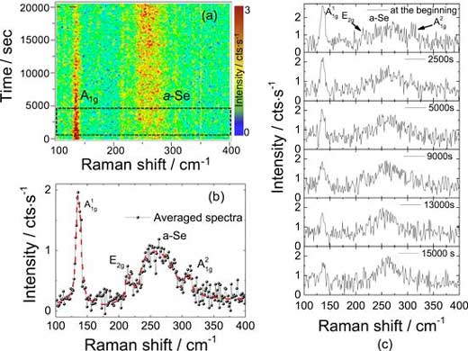
Raman spectrum of 8 L GaSe taken at two different times during time evolution map. (a) Red dashed line is drawn as the guide for the eye. The constant intensity ratio peaks indicates that oxidation stops approximately after 16 500 s. Thickness dependent Raman spectrum of GaSe for oxidation investigation. (b) Each spectrum was taken with 700 s × 3 of accumulation time. (Image: Tomsk Polytechnic University)
One of the promising areas of modern materials science is the study of two-dimensional (2D) materials, i.e. thin films consisting of one or several atomic layers. 2D materials due to their electrical superconductivity and strength could be a basis for modern nanoelectronics. Optic applications in nanoelectronics require advanced materials capable of ‘generating’ great electron fluxes upon light irradiation. Gallium selenide (GaSe) is one of the 2D semiconductors that can cope with this problem most efficiently.
‘Some research teams abroad tried to create electronic devices based on GaSe. However, despite extensive theoretical studies of this material, which were published in major scientific journals, the stability of the material in real devices remained unclear,’ says Prof. Raul Rodriguez, the Department of Lasers and Lighting Engineering.
The research team revealed the reasons behind this. They studied GaSe by means of Raman spectroscopy and x-ray photoelectron spectroscopy that allowed proving the existence of chemical bonds between gallium and oxygen. Photoluminescence in oxidized substance is absent that also proves the formation of oxides. It means that the scientists revealed that GaSe oxidizes quickly in air and loses its electrical conductivity necessary for creating nanoeletronic devices.
‘GaSe monolayers become oxidized almost immediately after being exposed to air. Further research of GASe stability in air will allow making proposals how to protect it and maintain its optoelectronic properties,’ emphasize the authors.
According to Prof. Rodriguez, for GaSe not to lose its unique properties it should be placed in a vacuum or inert environment. For example, it can be applied in encapsulated devices that are vacuum-manufactured and then covered with a protective layer eliminating air penetration.
This method can be used to produce next generation optoelectronics, detectors, light sources and solar batteries. Such devices of ultra-small sizes will have very high quantum efficiency, i.e. they will be able to generate large electron fluxes under small external exposure.
Source: Tomsk University

Strângerea memoriei: Materialele inovatoare de tip prototip sunt viitorul stocării datelor(Straining the memory: Prototype strain engineered materials are the future of data storage)

Când atomii de la interfață sunt dezordonați, materialul are o rezistență electrică ridicată, în timp ce interfața comandată are o rezistență electrică scăzută. Deoarece numai interfața comută, un subset de straturi din material poate rămâne neschimbat și cristalin. Aceasta înseamnă că interfața poate fi proiectată de straturile fără comutare – întreaga structură nu trebuie să treacă într-o stare dezordonată. Acest lucru face superlattica foarte diferită de aliajele de memorie cu schimbări de fază nestructurate, cum ar fi aliajul Ge 2 Sb 2 Te 5 .

Posted: Sep 20, 2017

Straining the memory: Prototype strain engineered materials are the future of data storage

(Nanowerk News) Researchers from the Singapore University of Technology and Design (SUTD) and Shanghai Institute of Microsystems and Information Technology have nano-engineered a superlattice data storage material. Data is recorded at the interfaces of the superlattice layers.

When the atoms at the interface are disordered, the material has a high electrical resistance while the ordered interface has a low electrical resistance. Since only the interface switches, a subset of layers within the material can remain unchanged and crystalline. This means that the interface can be engineered by the non-switching layers – the entire structure need not switch into a disordered state. This makes the superlattice very different to unstructured phase change memory alloys, such as the Ge2Sb2Te5 alloy.
 comparison of the electrical switching current and switching times for the strained superlattices interfacial phase change memory with other state-of-the-art phase change memory materials
A comparison of the electrical switching current and switching times for the strained superlattices interfacial phase change memory with other state-of-the-art phase change memory materials. (Image: Zhou et al.) (click on image to enlarge)
The authors showed in a paper published in Nano Futures („Avalanche atomic switching in strain engineered Sb2Te3–GeTe interfacial phase-change memory cells”) that fast switching in these nanostructured materials is due to avalanche atomic switching at the interface.
The first atom that switches requires a large amount of energy, but subsequent atoms require less energy. As more atoms switch, the energy required for subsequent atoms to switch is lowered. This leads to an exponential increase in the switching probability with the number of atoms switching.
Zhou et al showed that the energy for the first atom to switch can be engineered by straining the layer interfaces. The research team created prototype memory devices, which exploit this effect that outperformed state-of-the-art phase change memory devices. The switching voltage, current, and switching time are substantially reduced while the electrical resistance changes by a factor of 500. Thus these prototype devices are faster and more efficient than current competing technologies.
One of the members of the research team, Assistant Professor Robert Simpson, said: „The superlattices devices are remarkably energy efficient. We foresee this technology impacting new 3D memory architectures, such as Intel’s 3D x-point. We are now building on the success of these data storage materials by optimising similar phase change materials for switchable nano photonics applications.”
Source: Singapore University of Technology and Design

Grafenul și alte nanomateriale de carbon pot înlocui metalele rare(Graphene and other carbon nanomaterials can replace scarce metals)

Nanomaterialele de carbon constau exclusiv sau în principal din carbon și sunt materiale puternice cu o bună conductivitate. Mai multe metale rare au proprietăți similare. Metalele se găsesc, de exemplu, în cabluri, ecrane subțiri, ignifuge, protecție la coroziune și condensatoare.
Rickard Arvidsson și Björn Sandén de la Universitatea de Tehnologie din Chalmers au investigat dacă nanoparticulele de carbon, grafena, fullerenele și nanotuburile de carbon au potențialul de a înlocui 14 metale rare în principalele domenii de aplicare (vezi tabelul din imaginea atașată). Ei au găsit soluții potențiale bazate pe tehnologie pentru a înlocui metalele cu nanomateriale de carbon pentru toate aplicațiile, cu excepția aurului din bijuterii. Metalele pe care le avem cel mai aproape de a putea înlocui sunt indiu, galiu, beriliu și argint.

Posted: Sep 19, 2017

Graphene and other carbon nanomaterials can replace scarce metals

(Nanowerk News) Scarce metals are found in a wide range of everyday objects around us. They are complicated to extract, difficult to recycle and so rare that several of them have become „conflict minerals” which can promote conflicts and oppression. A survey at Chalmers University of Technology now shows that there are potential technology-based solutions that can replace many of the metals with carbon nanomaterials, such as graphene (Journal of Cleaner Production, „Carbon nanomaterials as potential substitutes for scarce metals”).

They can be found in your computer, in your mobile phone, in almost all other electronic equipment and in many of the plastics around you. Society is highly dependent on scarce metals, and this dependence has many disadvantages.
Scarce metals such as tin, silver, tungsten and indium are both rare and difficult to extract since the workable concentrations are very small. This ensures the metals are highly sought after – and their extraction is a breeding ground for conflicts, such as in the Democratic Republic of the Congo where they fund armed conflicts.
In addition, they are difficult to recycle profitably since they are often present in small quantities in various components such as electronics.
Graphene and Other Carbon Nanomaterials Can Replace Scarce Metals
Scarce metals are found in a wide range of everyday objects around us. A survey at Chalmers University of Technology now shows that there are potential technology-based solutions that can replace many of the metals with carbon nanomaterials, such as graphene. (Image: Jonas Sandwall) (click on image to enlarge)
Rickard Arvidsson and Björn Sandén, researchers in environmental systems analysis at Chalmers University of Technology, have now examined an alternative solution: substituting carbon nanomaterials for the scarce metals. These substances – the best known of which is graphene – are strong materials with good conductivity, like scarce metals.
„Now technology development has allowed us to make greater use of the common element carbon,” says Sandén. „Today there are many new carbon nanomaterials with similar properties to metals. It’s a welcome new track, and it’s important to invest in both the recycling and substitution of scarce metals from now on.”
The Chalmers researchers have studied the main applications of 14 different metals, and by reviewing patents and scientific literature have investigated the potential for replacing them by carbon nanomaterials. The results provide a unique overview of research and technology development in the field.
According to Arvidsson and Sandén the summary shows that a shift away from the use of scarce metals to carbon nanomaterials is already taking place.
„There are potential technology-based solutions for replacing 13 out of the 14 metals by carbon nanomaterials in their most common applications. The technology development is at different stages for different metals and applications, but in some cases such as indium and gallium, the results are very promising,” Arvidsson says.
„This offers hope,” says Sandén. „In the debate on resource constraints, circular economy and society’s handling of materials, the focus has long been on recycling and reuse. Substitution is a potential alternative that has not been explored to the same extent and as the resource issues become more pressing, we now have more tools to work with.”
The research findings were recently published in the Journal of Cleaner Production. Arvidsson and Sandén stress that there are significant potential benefits from reducing the use of scarce metals, and they hope to be able to strengthen the case for more research and development in the field.
„Imagine being able to replace scarce metals with carbon,” Sandén says. „Extracting the carbon from biomass would create a natural cycle.”
„Since carbon is such a common and readily available material, it would also be possible to reduce the conflicts and geopolitical problems associated with these metals,” Arvidsson says.
At the same time they point out that more research is needed in the field in order to deal with any new problems that may arise if the scarce metals are replaced.
„Carbon nanomaterials are only a relatively recent discovery, and so far knowledge is limited about their environmental impact from a life-cycle perspective. But generally there seems to be a potential for a low environmental impact,” Arvidsson says.

Facts

Carbon nanomaterials consist solely or mainly of carbon, and are strong materials with good conductivity. Several scarce metals have similar properties. The metals are found, for example, in cables, thin screens, flame-retardants, corrosion protection and capacitors.
Rickard Arvidsson and Björn Sandén at Chalmers University of Technology have investigated whether the carbon nanomaterials graphene, fullerenes and carbon nanotubes have the potential to replace 14 scarce metals in their main areas of application (see table in attached image). They found potential technology-based solutions to replace the metals with carbon nanomaterials for all applications except for gold in jewellery. The metals which we are closest to being able to substitute are indium, gallium, beryllium and silver.
Source: Chalmers University of Technology


O nouă abordare a impulsurilor ultrascurte de lumină(A new approach to ultrafast light pulses)

Deoarece reacția materialului este atât de puternic influențată de apropierea exactă a substratului metalic din apropiere, astfel de sisteme ar putea fi de asemenea folosite pentru instrumente de măsurare foarte precise. „Interacțiunea este redusă ca o funcție a mărimii decalajului, astfel încât aceasta ar putea fi acum utilizată dacă vrem să măsuram apropierea unei suprafețe”, spune Fang.
Pe măsură ce echipa își continuă studiile cu privire la aceste materiale, următorul pas este de a studia efectele pe care ar putea avea modelul suprafeței metalice, deoarece testele au utilizat până acum numai suprafețe plane.

Posted: Sep 18, 2017

A new approach to ultrafast light pulses

(Nanowerk News) Two-dimensional materials called molecular aggregates are very effective light emitters that work on a different principle than typical organic light-emitting diodes (OLEDs) or quantum dots. But their potential as components for new kinds of optoelectronic devices has been limited by their relatively slow response time. Now, researchers at MIT, the University of California at Berkeley, and Northeastern University have found a way to overcome that limitation, potentially opening up a variety of applications for these materials.

The findings are described in the journal Proceedings of the National Academy of Sciences(„Ultrafast fluorescent decay induced by metal-mediated dipole–dipole interaction in two-dimensional molecular aggregates”), in a paper by MIT associate professor of mechanical engineering Nicholas X. Fang, postdocs Qing Hu and Dafei Jin, and five others.
light strikes a molecular lattice deposited on a metal substrate
In this image, light strikes a molecular lattice deposited on a metal substrate. The molecules can quickly exchange energy with the metal below, a mechanism that leads to a much faster response time for the emission of fluorescent light from the lattice. (Image: MIT)
The key to enhancing the response time of these 2-D molecular aggregates (2DMA), Fang and his team found, is to couple that material with a thin layer of a metal such as silver. The interaction between the 2DMA and the metal that is just a few nanometers away boosts the speed of the material’s light pulses more than tenfold.
These 2DMA materials exhibit a number of unusual properties and have been used to create exotic forms of matter, known as Bose-Einstein condensates, at room temperature, while other approaches required extreme cooling. They have also been applied in technologies such as solar cells and light-harvesting organic antennas. But the new work for the first time identifies the strong influence that a very close sheet of metal can have on the way these materials emit light.
In order for these materials to be useful in devices such as photonic chips – which are like semiconductor chips but carry out their operations using light instead of electrons – „the challenge is to be able to switch them on and off quickly,” which had not been possible before, Fang says.
With the metal substrate nearby, the response time for the light emission dropped from 60 picoseconds (trillionths of a second) to just 2 picoseconds, Fang says: „This is pretty exciting, because we observed this effect even when the material is 5 to 10 nanometers away from the surface,” with a spacing layer of polymer in between. That’s enough of a separation that fabricating such paired materials in quantity should not be an overly demanding process. „This is something we think could be adapted to roll-to-roll printing,” he says.
If used for signal processing, such as sending data by light rather than radio waves, Fang says, this advance could lead to a data transmission rate of about 40 gigahertz, which is eight times faster than such devices can currently deliver. This is „a very promising step, but it’s still very early” as far as translating that into practical, manufacturable devices, he cautions.
The team studied only one of the many kinds of molecular aggregates that have been developed, so there may still be opportunities to find even better variations. „This is actually a very rich family of luminous materials,” Fang says.
Because the responsiveness of the material is so strongly influenced by the exact proximity of the nearby metal substrate, such systems could also be used for very precise measuring tools. „The interaction is reduced as a function of the gap size, so it could now be used if we want to measure the proximity of a surface,” Fang says.
As the team continues its studies of these materials, one next step is to study the effects that patterning of the metal surface might have, since the tests so far only used flat surfaces. Other questions to be addressed include determining the useful lifetimes of these materials and how they might be extended.
Fang says a first prototype of a device using this system might be produced „within a year or so.”
Source: By David L. Chandler, Massachusetts Institute of Technology

Fizicienii prezic o semi-metalicitate nemetalică( Physicists predict nonmetallic half-metallicity )

Spre deosebire de un metal obișnuit, într-un material semi-metalic, electronii cu o singură orientare în rotație – de exemplu, spin-up – participă la curentul electric. În ceea ce privește electronii spin-down, energia lor este prea mare și, prin urmare, nu pot purta curent de încărcare. Aceasta înseamnă că, atunci când curentul trece printr-o jumătate de metal, este generat și un curent polarizat în spin. Dar tronica spin-valley încearcă să manipuleze nu numai o populație de electroni spin-polarizată în actualul dar și așa-numitul index de vale.Pentru un material cu o undă de densitate pentru a deveni o jumătate de metal, este nevoie de un tratament special cunoscut sub numele de dopaj. Aceasta implică încorporarea electronilor sau a găurilor în izolator. Alexandru Rozhkov, co-autor al lucrării și cercetător la Departamentul de Probleme de Fizică și Energetică al MIPT, explică faptul că un sistem poate fi dopat prin supunerea lui la un câmp electric extern sau la modificări chimice de vrac sau de suprafață: „Pentru fiecare sistem , trebuie selectat un tip adecvat de atomi de dopaj – cum ar fi azot, fosfor sau alt element. Prin înlocuirea atomilor din sistemul gazdă cu impuritățile care dau sau acceptă electroni de conducere, este indusă o schimbare a proprietăților materialului original. ”

Posted: Sep 14, 2017

Physicists predict nonmetallic half-metallicity

(Nanowerk News) A team of researchers from the Moscow Institute of Physics and Technology (MIPT) and the Institute for Theoretical and Applied Electrodynamics (ITAE) of the Russian Academy of Sciences (RAS), in collaboration with a colleague from RIKEN (an institute for physical and chemical research in Japan), has provided theoretical proof of the existence of a new class of materials. It was suggested that such systems be referred to as ‘spin-valley half-metals.’

The paper was published in the journal Physical Review Letters („Spin-Valley Half-Metal as a Prospective Material for Spin Valleytronics”). The discovery will find use in implantable electronics, alongside devices based on graphene, nanotubes, and a number of other promising materials.
The microscopic mechanism proposed by the researchers differs significantly from the usual half-metal model based on a strong electron-electron interaction. This might give rise to a new direction in search for ‘nonmetallic’ half-metals, i.e., those that do not contain atoms of transition metals, such as nickel, manganese, and lanthanum. These would come in handy in implantable devices and systems. The authors use the term ‘spin-valley-tronics’ to refer to the possible alternative to traditional electronics.
Since the invention of the electron tube, the world has seen electronics exhaust most of its possibilities. It would be highly challenging to continue increasing the number of transistors or microprocessor clock rate. That is why researchers around the globe are exploring new possibilities. One of them is spintronics which makes use of electron spins and already has some important practical applications. Around the turn of the century, the use of giant magnetoresistance materials in magnetic field sensors (used to read data in hard disk drives) has enabled the storage of much larger amounts of data on HDDs.
Researchers all over the world are working on new spintronic devices, and half-metals are believed to have great potential. They were first predicted based on computer simulations and later proved to exist experimentally. Unlike a usual metal, in a half-metallic material, electrons of only one spin orientation — e.g., spin up — participate in the electric current. As for spin-down electrons, their energy is too high, and therefore they cannot carry charge current. This means that when the current is passed through a half-metal, a spin-polarized current is generated as well. But spin-valley-tronics seeks to manipulate not only a spin-polarized population of electrons in the current but also the so-called valley index.
electronic spin
Fig. 1. The term ‘spin’ refers to the intrinsic angular momentum of a particle. The spin of a particle has both a magnitude and a direction. In the case of the electron, the magnitude is 1/2 times Planck’s constant, and the direction is either up or down. (Image: MIPT)
The term ‘valley’ is borrowed from semiconductor physics. Mathematically, the excitation energy in a solid is expressed by E (κ, n), where κ is the momentum of the electron and n is the zone index, i.e., a discrete quantum property of the state of the electron. This function may look rather odd, and in the case of several minimums with comparable excitation energies, one can speak of the presence of multiple ‘valleys’.
With certain reserve, one could say that electrons whose states correspond to one of the valleys do not interact with electrons from another valley. Such an ensemble of electrons can carry not only spin and charge, but also a distinct value called the valley index.
electron and hole energy is plotted against momentum
In the figure, electron and hole energy is plotted against momentum. (The four black curves correspond to two projections of electron spin and two projections of hole spin.) The thick curve corresponds to electron states capable of conducting an electric current (forming a Fermi surface). Depending on the mutual orientation of the spins of electrons (blue arrows) and holes (red arrows) on the Fermi surface, the system is either an ordinary half-metal (c) or a spin-valley half-metal (d). (Image: MIPT)
The valley index can be used to transfer information with the help of valley currents – in this regard, the valley index is quite similar to spin. Research in this direction is currently being carried out by several groups, which implies that the ideas proposed in the publication are not pure abstractions. The idea of using the valley index is certainly not a new one, but what the researchers did is, they theoretically proved the existence of a novel class of materials for use in spin-valley-tronics.

So what’s new?

The half-metals available to the researchers all contain atoms of transition metals: nickel, manganese, or lanthanum, etc. The team of researchers, which included physicists from Russia and Japan, has demonstrated a theoretical mechanism for achieving half-metallicity that requires no transition metal atoms. This possibility would have a number of useful applications, including in implantable devices.
The physicists suggest that ‘nonmetallic half-metals’ be obtained from a special class of dielectric materials called charge- or spin-density wave insulators. The term charge- or spin-density wave refers to a state with periodic microscopic regions with nonzero average charge (spin) in the material. Theorists describe such systems as a quantum condensate of electron-hole pairs. For a pair of this kind to form, two valleys are required: One provides electrons, the other provides holes. It is the presence of two valleys in the original system that gives rise to spin-valley half-metallicity.
In semiconductor physics, a ‘hole’ is a quasiparticle that is considered to have a positive charge.
For a material with a density wave to become a half-metal, it requires a special treatment known as doping. This involves the incorporation of electrons or holes into the insulator. Alexander Rozhkov, a co-author of the paper and a researcher at MIPT’s Department of Problems of Physics and Energetics, explains that a system can be doped by subjecting it to an external electric field or chemical modifications of bulk or surface: ‘For each system, a suitable type of doping atoms – such as nitrogen, phosphorus, or some other element – needs to be selected. By replacing atoms of the host system with impurities donating or accepting conduction electrons, a change in the properties of the original material is induced.’
The possibility of doping materials with density waves has been discussed in the literature for a long time. Thus, among articles cited in the newly published paper are those dating back to 1970s. The systems dealt with by the researchers have been shown to have various phases, including spatially inhomogeneous (for example, states with the so-called electronic phase separation, and the phases with domain walls, often called ‘stripes’). Now, the unexpected discovery of two new phases – regular and spin-valley half-metallicity – has been made.
Source: Moscow Institute of Physics and Technology

Read more: Physicists predict nonmetallic half-metallicity