
| Posted: Sep 27, 2017 | |
Progress achieved towards mass producing carbon nanotube sheets(Nanowerk News) Researchers at the Masdar Institute have recently announced a breakthrough approach to producing carbon nanotube (CNT) sheets, known as ‘buckypaper,’ through a scalable, low-cost and simple technique. The novel fabrication method could help bring game-changing buckypaper applications a step closer towards cost-effective commercialization. |
|
| “Being able to produce buckypaper in a scalable way like this has not been demonstrated before. This new technique could boost the development of market-ready applications, including high-power lithium-ion batteries and low-cost vanadium-redox-flow batteries,” said Dr. Rahmat Susantyoko, postdoctoral researcher from the Mechanical Engineering Department. | |
| Dr. Susantyoko was first author of a paper that describes the new technique, called Surface-Engineered Tape-Cast (SETC), which was published last month in the Journal of Materials Chemistry A („A surface-engineered tape-casting fabrication technique toward the commercialisation of freestanding carbon nanotube sheets”). | |
 |
|
| Buckypaper | |
| CNTs are sheets of carbon that have been rolled into tubes, measuring 100,000 times smaller than the diameter of human hair. Their exceptional electrical, chemical, thermal and mechanical properties make them an ideal material for countless applications, including in energy storage, computer chips, and sensors. The revolutionary potential of CNTs in materials engineering is reflected by the projected growth of its market value, which is expected to reach US$8.7 billion by 2022, according to market analysts Markets and Markets. Buckypaper is a thin sheet made of aggregated carbon nanotubes. | |
| Despite the technical potential of buckypaper, a critical problem continues to hinder its development for CNT applications. The difficulty of converting CNTs from their original fine, dust-like powdery state, to a solid, thin film of grouped CNTs remains a key challenge. | |
| CNTs in buckypaper form are much easier for engineers to manipulate. In their macroscopic manifestation, CNTs can be processed and developed into useful materials for a broader range of applications. While many innovative buckypaper-based applications have been developed in recent years, they failed to achieve broad commercialization because they lacked a scalable and cost-effective buckypaper fabrication process. | |
| “Common buckypaper fabrication methods used today are membrane filtration and chemical vapor deposition. However both methods have severe limitations, with membrane filtration restricting the size of the produced buckypaper to the size of the membrane and apparatus used, and chemical vapor deposition being exceedingly expensive,” Dr. Susantyoko explained. | |
| Addressing the need for a low-cost, scalable fabrication method, Masdar Institute’s SETC technique offers a novel solution that leverages tape-casting – a method traditionally used to coat a CNT film over a substrate – that overcomes the current technological limitations that have prevented low-cost, scalable buckypaper fabrication till now. | |
| “Our technique utilizes tape-casting with a special type of substrate, which we engineered in the lab, that allows us to easily peel off the buckypaper from the supporting substrate, resulting in a free-standing buckypaper film,” Dr. Susantyoko said. | |
| Identifying the ideal substrate that would allow the buckypaper to easily peel off was the biggest challenge. Through investigation, the team discovered that buckypaper sticks to smooth and randomly-patterned rough surfaces, but separates from a special kind of surface that has a rough structure composed of micro-sized pyramids. | |
| “We realized that the surface morphology of substrate and dissimilarity in surface energy of CNT–substrate play important roles in affecting the ability to easily peel off the CNT film,” Dr. Susantyoko added. He explained that the unique morphology and high surface area created by the micro-pyramids enabled the easy separation of the CNT sheet. | |
| To demonstrate the effectiveness of their SETC buckypaper fabrication technique, the team used it to produce a buckypaper-based cathode for a high-power lithium-ion battery. Now, the team is enhancing their SETC method to produce an even higher-powered cathode, which is intended to be used for space applications. | |
| By providing materials scientists with a scalable, low-cost and simple method to fabricate CNT sheets, Masdar Institute researchers are helping to bring the game-changing CNT innovations being developed in labs across the world to the market. |
Progresele înregistrate în procesul de obținere a foilor de nanotuburi de carbon în masă(Progress achieved towards mass producing carbon nanotube sheets)
CNT-urile sunt foi de carbon care au fost laminate în tuburi, măsurând 100.000 de ori mai mici decât diametrul părului uman. Proprietățile lor electrice, chimice, termice și mecanice excepționale le fac un material ideal pentru nenumărate aplicații, inclusiv pentru stocarea energiei, cipuri de calculator și senzori. Potențialul revoluționar al CNT-urilor în ingineria materialelor se reflectă în creșterea prognozată a valorii de piață, care se așteaptă să ajungă la 8,7 miliarde de dolari până în 2022, potrivit analistilor de piață Markets and Markets. Buckypaper este o foaie subțire din nanotuburi de carbon agregate.
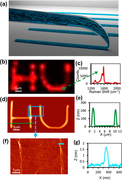 Controlled direct drawing of SWCNTs on SiO