| Source: University of Bristol |
Read more: Shape-changing metamaterial developed using Kirigami technique
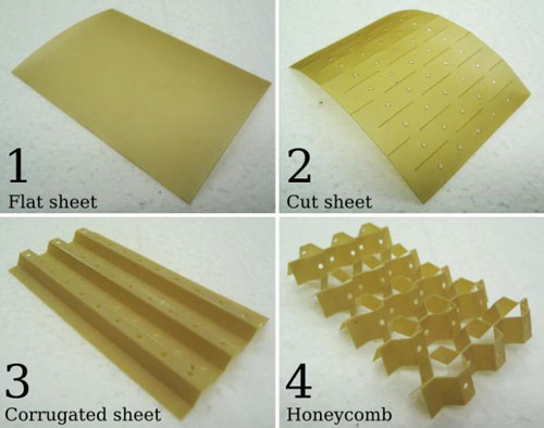
au dezvoltat un nou metamaterial care schimba forma folosind Kirigami, arta antica japoneza de taiere si pliere a hartiei pentru a obtine forme 3D.Metamaterialele sunt o clasă de materiale proiectate pentru a produce proprietăți care nu apar în mod natural. În prezent, metamaterialele sunt folosite pentru a face absorbanți artificiali și vibrații artificiali și senzori de înaltă performanță. Kirigami poate fi aplicat pentru a transforma materialele din tablă bidimensională în forme tridimensionale complexe cu o gamă mai largă de geometrii decât origami „clasice”.
| Source: University of Bristol |
Read more: Shape-changing metamaterial developed using Kirigami technique
Unul dintre cele mai fierbinți materiale noi este o clasă de substanțe solide poroase, cunoscute sub numele de cadre metalice organice sau MOF. Aceste materiale artificiale au fost introduse în anii 1990, iar cercetătorii din întreaga lume lucrează la modalități de utilizare a acestora ca bureți moleculari pentru aplicații cum ar fi stocarea hidrogenului, sechestrarea carbonului sau fotovoltaica. Acum, o descoperire surprinzătoare a oamenilor de știință din Canada și Rusia relevă faptul că MF există, de asemenea, în natură – deși sub formă de minerale rare găsite până acum numai în minele de cărbune din Siberia.
| Posted: Aug 05, 2016 | |
Metal-organic frameworks found to exist in nature(Nanowerk News) One of the hottest new materials is a class of porous solids known as metal-organic frameworks, or MOFs. These man-made materials were introduced in the 1990s, and researchers around the world are working on ways to use them as molecular sponges for applications such as hydrogen storage, carbon sequestration, or photovoltaics. Now, a surprising discovery by scientists in Canada and Russia reveals that MOFs also exist in nature – albeit in the form of rare minerals found so far only in Siberian coal mines. |
|
| The finding, published in the journal Science Advances („Minerals with metal-organic framework structures”), „completely changes the normal view of these highly popular materials as solely artificial, ‘designer’ solids,” says senior author Tomislav Friscic, an associate professor of chemistry at McGill University in Montreal. „This raises the possibility that there might be other, more abundant, MOF minerals out there.” | |
![]() |
|
| An aggregate of synthetic zhemchuzhnikovite, prepared by Igor Huskić, McGill University) | |
| The twisting path to the discovery began six years ago, when Friscic came across a mention of the minerals stepanovite and zhemchuzhnikovite in a Canadian mineralogy journal. The crystal structure of the minerals, found in Russia between the 1940s and 1960s, hadn’t been fully determined. But the Russian mineralogists who discovered them had analyzed their chemical composition and the basic parameters of their structures, using a technique known as X-ray powder diffraction. To Friscic, those parameters hinted that the minerals could be structurally similar to a type of man-made MOF. | |
| His curiosity piqued, Friscic began looking for samples of the rare minerals, reaching out to experts, museums and vendors in Russia and elsewhere. After a promising lead with a mining museum in Saint Petersburg failed to pan out, Igor Huskic, a graduate student in the Friscic research group at McGill turned his attention to synthesizing analogues of the minerals in the lab – and succeeded. But a major journal last year declined to publish the team’s work, in part because the original description of the minerals had been reported in a somewhat obscure Russian mineralogical journal. | |
| Then, the McGill chemists caught a break: with the help of a crystallographer colleague in Venezuela, they connected with two prominent Russian mineralogists: Sergey Krivovichev, a professor at Saint Petersburg State University, and Prof. Igor Pekov of Lomonosov Moscow State University. | |
| Krivovichev and Pekov were able to obtain the original samples of the two rare minerals, which had been found decades earlier in a coal mine deep beneath the Siberian permafrost. The Russian experts were also able to determine the crystal structures of the minerals. These findings confirmed the McGill researchers’ initial results from their lab synthesis. | |
![]() |
|
| Fragment of the crystal structure of the natural zhemchuzhnikovite mineral. | |
| Stepanovite and zhemchuzhnikovite have the elaborate, honeycomb-like structure of MOFs, characterized at the molecular level by large voids. The two minerals aren’t, however, representative of the hottest varieties of MOFs – those that are being developed for use in hydrogen-fueled cars or to capture waste carbon dioxide. | |
| As a result, Friscic and his collaborators are now broadening their research to determine if other, more abundant minerals have porous structures that could make them suitable for uses such as hydrogen storage or even drug delivery. | |
| In any event, the discovery of MOF structures in the two rare minerals already is „paradigm-changing” Friscic says. If scientists had been able to determine those structures in the 1960s, he notes, the development of MOF materials „might have been accelerated by 30 years.” |
| Source: McGill University |
Read more: Metal-organic frameworks found to exist in nature
Materialul este silicena, cea mai subțire formă posibilă de siliciu, compusă dintr-un strat bidimensional de cristale de siliciu.
Electronii se deplasează ultra-rapid în siliciu, reducând energia necesară pentru acționarea dispozitivelor electronice și deschizând calea pentru electronice și mai mici, flexibile, transparente și cu consum redus de energie.
| Posted: Aug 01, 2016 | |
Peeling off the silicene layers for new electronics(Nanowerk News) Much like an overcooked dinner, the next so-called wonder material for next-generation electronics has been ‘stuck to the pan’ until researchers at the UOW’s Institute for Superconducting and Electronic Materials (ISEM) came up with a breakthrough solution. |
|
| The material is silicene, the thinnest possible form of silicon, comprised of a two-dimensional layer of silicon crystals. | |
| Electrons move ultrafast in silicene, reducing the energy required to drive electronic devices and paving the way for even smaller, flexible, transparent and low-energy-cost electronics. | |
| Until now, silicene has been ‘grown’ on a metal surface, but researchers had no proven way of freeing it from the substrate to create a freestanding material that could then be incorporated into electronic devices and components. | |
| ISEM Research Fellow Dr Yi Du and his team have used oxygen to separate a single-atom thick layer of silicon from its surface, overcoming the key hurdle preventing the production of a material with potential to supercharge electronics. | |
| “We know silicene crystals prefer to firmly attach on the metallic substrate and because they are too thin to be peeled off by any mechanical tools, it’s impossible to remove them from the substrate,” Dr Du said. | |
| Researchers have experimented with the idea of using ‘chemical scissors’ to break the bond between silicene and the substrate and the breakthrough for Dr Du and his team came through using oxygen molecules as chemical scissors to cut the silicene from its substrate. | |
| The work, supported by the Australian Research Council (ARC), involves several special techniques that can be done only at ISEM with the help of its powerful tools, including a scanning tunneling microscope, which creates an ultra-high vacuum environment about a hundred times higher than the vacuum level experienced in orbit at the International Space Station. | |
| “Because the vacuum levels are so high, we can inject the oxygen molecules into the chamber and they become a ‘molecular flux’ that follows a straight pathway,” Dr Du said. | |
| “This allows us to direct these molecules precisely into the silicene layers, acting like scissors to separate the silicene.” | |
![]() |
|
| Injecting oxygen molecules precisely into the silicene layers creates ‘scissors’ that separate the silicene from the metal surface. | |
| The result is a layer of freestanding silicene – with an appearance much like a honeycomb lattice – that could be transferred to an insulating substrate to make advanced transistors. | |
| The theory for two-dimensional silicene was introduced in 1994 but it wasn’t until 2012 that scientists, including a team at UOW, successfully fabricated silicene in the lab. | |
| Silicene is emerging player in the super-materials category, alongside graphene, which is a single-atom thick layer of carbon. | |
| Graphene has been shown to be the fastest conductor of electricity yet found, faster than commonly used silicon. Graphene can’t be switched between on and off states of conductivity. | |
| This makes it unsuitable for applications such as transistors. Because silicon and carbon sit side-by-side on the periodic table, scientists were inspired to investigate if silicon’s atomic properties could be similarly revolutionary but more easily exploited because of its compatibility with existing silicon-based electronics. | |
| “This work solves the long-lasting problem of isolating this super material for further device development. It challenges the entire scientific literature on silicene since its discovery,” Dr Du said. | |
| “These findings are relevant for the future design and application of silicene-based nano-electronic and spintronic devices.” | |
| The research was published recently in the journal Science Advances („Quasi-freestanding epitaxial silicene on Ag(111) by oxygen intercalation”) and ACS Central Science („Observation of van Hove Singularities in Twisted Silicene Multilayers”) and is the result of collaboration between Australian and Chinese researchers including Professor Jijun Zhao, from the Dalian University of Technology and Dr Jiaou Wang at the Beijing Synchrotron Radiation Facility (Chinese Academy of Sciences). |
| Source: University of Wollongong |
Read more: Peeling off the silicene layers for new electronics
Absorbția solară în bandă largă a fost realizată anterior utilizând rezonatoare metal-izolator-metal (sau MIM), care constau dintr-un izolator sandwich între un fund gros și un strat superior subțire, fiecare realizat din metale precum cromul și aurul. Componentele metalice utilizate în rezonanții MIM au puncte de topire relativ scăzute – temperaturi care sunt reduse în continuare atunci când materialele sunt în straturi foarte subțiri, ca în rezonatoare, datorită unui fenomen numit depresie la punctul de topire, în care punctul de topire al unui material Scade în jos ca dimensiunile de scădere a materialului. Metalele din rezonanții standard MIM se topesc la aproximativ 500 de grade Celsius, împiedicând utilizarea lor în celulele solare.
Sunt rezistente la căldură, inclusiv șoc termic, și prezintă proprietăți fizice și chimice stabile la temperaturi ridiccate
| Posted: Aug 01, 2016 | |
New high-temperature device captures a broader solar wavelength spectrum(Nanowerk News) The photovoltaic (PV) cells in traditional solar cells convert sunlight efficiently within a narrow range of wavelengths determined by the material used in the PV cells. This limits their efficiency, as long wavelengths of sunlight are not converted at all and the energy of short wavelength light is largely wasted. Scientists have sought to increase the efficiency of photovoltaics by creating „multi-junction” solar cells, made from several different semiconductor materials that absorb at varying wavelengths of light. The problem is, such multi-junction cells are expensive to make. |
|
| Broadband solar absorption previously has been achieved using metal-insulator-metal (or MIM) resonators, which consist of an insulator sandwiched between a thick bottom and a thin top layer, each made of metals like chromium and gold. The metal components used in MIM resonators have relatively low melting points–temperatures that are reduced further when the materials are in very thin layers, as in the resonators, because of a phenomenon called melting point depression, in which the melting point of a material scales down as the dimensions of the material decrease. The metals in standard MIM resonators melt at around 500 degrees Celsius, hindering their usefulness in solar cells. | |
![]() |
|
| The schematic energy flow of standard and solar thermophotovoltaic (STPV) systems. In standard solar cells, a PV cell is directly illuminated by the sun. Whereas in STPV systems (b), an absorber placed between the sun and PV cell is heated by absorbing the broad solar spectrum. A thermal emitter connected to the absorber converts the heat into narrowband thermal radiation that illuminates the PV cell. The inset represents the schematic of the multilayer broadband absorber device. (Image: Manohar Chirumamilla) | |
| Now a group of researchers in Denmark have discovered an alternative method to capture a broad spectrum of sunlight using a heat-resistant device made of tungsten and alumina layers that can be fabricated using inexpensive and widely available film-deposition techniques. The researchers describe their work and the new material in a paper published this week in the journal Optical Materials Express („Multilayer tungsten-alumina-based broadband light absorbers for high-temperature applications”). | |
| „They are resistant to heat, including thermal shock, and exhibit stable physical and chemical properties at high temperatures,” explained Manohar Chirumamilla of Aalborg University in Denmark, the first author of the new paper. This allows the absorbers to maintain their structural properties at very high temperatures. | |
| In experiments, the new absorbers were shown to operate at a temperature of 800 degrees Celsius and to absorb light of wavelengths ranging from 300 to 1750 nanometers, that is, from ultraviolet (UV) to near-infrared wavelengths. | |
| „MIM resonators absorbing in the spectral region from UV to near-infrared can be directly employed in different applications, such as solar TPV [thermophotovoltaic] /TPV systems and solar thermal systems,” Chirumamilla said. „Other potential applications include in so-called tower power plants, where concentrated solar light generates steam to drive a generator.” | |
| „This is the first step in utilizing the energy of the sun in a more efficient way than with current solar cells,” he added. „Using an emitter in contact with our absorber, the generated heat can then be used to illuminate a solar cell–which can then function more efficiently when it is placed directly in the sun.” |
| Source: The Optical Society |
Read more: New high-temperature device captures a broader solar wavelength spectrum
au creat cristale cubice de nitrură de galiu (GaN) cultivate pe un substrat de siliciu care sunt capabile să producă lumină verde puternică pentru lumina solidă avansată (Aplicată Physics Letters, „Maximizing Phiber Cubic Nitridium Gallium Acoperirea suprafeței pe siliciu cu nano-model (100) „).
Această lucrare este foarte revoluționară, deoarece deschide calea pentru noii emițători de lungime de undă verde care pot viza iluminatul solid solid avansat pe o platformă scalabilă CMOS-silicon prin exploatarea noului material, nitrida de galiu cubică „, a spus Can Bayram, profesor asistent de electricitate Și ingineria calculatoarelor din Illinois, care a început să investigheze acest material în timp ce la IBM TJ Watson Research Center acum câțiva ani.
| Posted: Jul 29, 2016 | |
New method for making green LEDs enhances their efficiency and brightness(Nanowerk News) Researchers at the University of Illinois at Urbana Champaign have developed a new method for making brighter and more efficient green light-emitting diodes (LEDs). Using an industry-standard semiconductor growth technique, they have created gallium nitride (GaN) cubic crystals grown on a silicon substrate that are capable of producing powerful green light for advanced solid-state lighting (Applied Physics Letters, „”Maximizing Cubic Phase Gallium Nitride Surface Coverage on Nano-patterned Silicon (100)”). |
|
![]() |
|
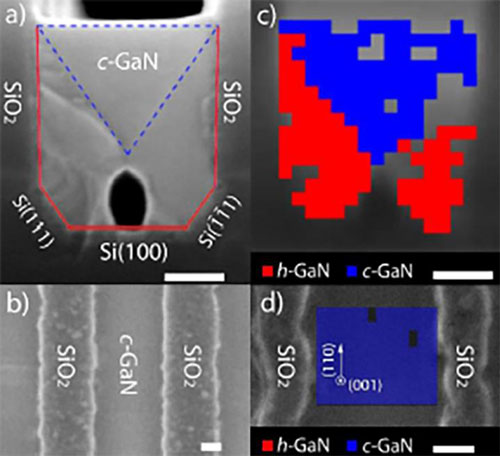
| A new method of cubic phase synthesis: Hexagonal-to-cubic phase transformation. The scale bars represent 100 nm in all images. (a) Cross sectional and (b) Top-view SEM images of cubic GaN grown on U-grooved Si(100). (c) Cross sectional and (d) Top-view EBSD images of cubic GaN grown on U-grooved Si(100), showing cubic GaN in blue, and hexagonal GaN in red. (Image: University of Illinois) | |
| „This work is very revolutionary as it paves the way for novel green wavelength emitters that can target advanced solid-state lighting on a scalable CMOS-silicon platform by exploiting the new material, cubic gallium nitride,” said Can Bayram, an assistant professor of electrical and computer engineering at Illinois who first began investigating this material while at IBM T.J. Watson Research Center several years ago. | |
| „The union of solid-state lighting with sensing (e.g. detection) and networking (e.g. communication) to enable smart (i.e. responsive and adaptive) visible lighting, is further poised to revolutionize how we utilize light. And CMOS-compatible LEDs can facilitate fast, efficient, low-power, and multi-functional technology solutions with less of a footprint and at an ever more affordable device price point for these applications.” | |
| Typically, GaN forms in one of two crystal structures: hexagonal or cubic. Hexagonal GaN is thermodynamically stable and is by far the more conventional form of the semiconductor. However, hexagonal GaN is prone to a phenomenon known as polarization, where an internal electric field separates the negatively charged electrons and positively charged holes, preventing them from combining, which, in turn, diminishes the light output efficiency. | |
| Until now, the only way researchers were able to make cubic GaN was to use molecular beam epitaxy, a very expensive and slow crystal growth method when compared to the widely used metal-organic chemical vapor deposition (MOCVD) method that Bayram used. | |
| Bayram and his graduate student Richard Liu made the cubic GaN by using lithography and isotropic etching to create a U-shaped groove on Si (100). This non-conducting layer essentially served as a boundary that shapes the hexagonal material into cubic form. | |
| „Our cubic GaN does not have an internal electric field that separates the charge carriers–the holes and electrons,” explained Liu. „So, they can overlap and when that happens, the electrons and holes combine faster to produce light.” | |
| Ultimately, Bayram and Liu believe their cubic GaN method may lead to LEDs free from the „droop” phenomenon that has plagued the LED industry for years. For green, blue, or ultra-violet LEDs, their light-emission efficiency declines as more current is injected, which is characterized as „droop.” | |
| „Our work suggests polarization plays an important role in the droop, pushing the electrons and holes away from each other, particularly under low-injection current densities,” said Liu, who was the first author of the paper. | |
| Having better performing green LEDs will open up new avenues for LEDs in general solid-state lighting. For example, these LEDs will provide energy savings by generating white light through a color mixing approach. Other advanced applications include ultra-parallel LED connectivity through phosphor-free green LEDs, underwater communications, and biotechnology such as optogenetics and migraine treatment. | |
| Enhanced green LEDs aren’t the only application for Bayram’s cubic GaN, which could someday replace silicon to make power electronic devices found in laptop power adapters and electronic substations, and it could replace mercury lamps to make ultra-violet LEDs that disinfect water. |
| Source: University of Illinois College of Engineering | |
Read more: New method for making green LEDs enhances their efficiency and brightness
Materialele în cauză au fost denumite substanțe magnetoionice magnetice cu proprietăți care depind de aranjamentul ionilor, care sunt atomi cu încărcătură electrică. Designerii de memorii ale calculatorului le plac pentru că funcționează diferit decât dispozitivele electronice tradiționale, care depind de mișcarea electronilor pentru a reprezenta 1s și 0s. Dar electronii nu rămân în dispozitivele tradiționale când moare puterea.
| Posted: Jul 22, 2016 | |
Valuable fundamentals of a stacked, cracked Jack of all trades(Nanowerk News) There is a crack in everything, Leonard Cohen sang; that’s how the light gets in. Now a team led by scientists from the National Institute of Standards and Technology (NIST) has explored the properties of a promising class of materials with new capabilities that depend on those cracks. Their results (Nature Communications, „Beyond the Interface: Structural and Magnetic Depth Profiles of Magneto-Ionic Heterostructures Beyond the Interface”) could help open the way for practical applications from nonvolatile computer memory to quick-dimming windows. |
|
![]() |
|
| This magneto-ionic thin film, made primarily of aluminum oxide (red), gadolinium oxide (green) and cobalt (blue), allows oxygen ions to travel up and down through spaces between the layers when pushed by an electric field. Controlling the ions’ movement could be useful in computer memory storage and a host of other applications. The depth of the film depicted in this figure is on the order of 10 nanometers. (Image: D. Gilbert/NIST) | |
| The materials in question have been dubbed magneto-ionics—magnetic substances with properties that depend on the arrangement of ions, which are atoms with an electric charge. Computer memory designers like them because they work differently than traditional electronic devices, which depend on the movement of electrons to represent 1s and 0s. But electrons don’t stick around in traditional devices when the power dies. | |
| Enter magneto-ionics, which are formed of several extremely thin layers of oxygen-containing crystalline particles stacked atop one another. These particles stack together, but have small gaps between them—allowing oxygen ions to move around among the particles. If layers of particles are set down as a thin film upon a surface, the ions can be moved up and down through the layers using an electric field, changing how they behave, even making magnetic layers lose their magnetism. Controlling whether the layers are magnetic or not potentially allows information storage as 1s and 0s. And once an ion moves to a new place, it tends to stay there, even without electricity. | |
| Other nonvolatile memory technologies exist, most notably hard drives and flash memory, but they work relatively slowly, have relatively short lifetimes and cannot be scaled up past a certain point—hard drives, for example, can only have so many layers. Ionic technologies would also operate slowly, but would be more scalable. | |
| The appeal of these magneto-ionic films goes far beyond data storage though, said NIST physicist Dustin Gilbert, because of the wide range of properties that can be changed by moving the oxygen ions around. | |
| “Controlling oxygen distributions offers an opportunity to tune virtually every property of a material: magnetic, structural, optical, mechanical or chemical, to name a few,” Gilbert said. “So in a broad sense, you could imagine any number of devices where we apply a voltage and entirely change their functional behavior. One possibility would be a window coating that changes from opaque to mirrored or transparent, so that you could let in sunlight with the flick of a switch.” | |
| Despite their broader potential, most of the research that has been performed up to now on magneto-ionics has been on extremely thin films just a few atomic layers thick. The NIST team set out to explore the behavior of the substantially thicker films that could be crucial for commercial applications. | |
| Their research, performed using neutron reflectometry at the NIST Center for Neutron Research, turned up a number of findings useful for the industry’s future. Smaller particles, for example, tend to make for better magneto-ionic films, as there are more cracks through which the oxygen ions can travel. Also, changing the chemical makeup and crystal structure of the particles and layers changes the properties of the film dramatically, meaning that particle engineering will be a major concern for manufacturers. | |
| Films’ properties also change after the oxygen ions make a few round-trips through the layers, raising questions about how long a device based on magneto-ionics could last. | |
| “We need to be able to switch these things back and forth a huge number of times,” Gilbert said. “Their durability and speed is improving fast, but there’s still a way to go. By better understanding oxygen movement in these devices, our work should help a lot with that. We’ve cracked the underlying physics of these films’ magnetic properties, which should enlighten engineers about how they can use them.” |
| Source: NIST |
Noile materiale funcționale sunt oxizi, inclusiv câteva tipuri de materiale care, până în prezent, nu au putut fi integrate pe așchii de siliciu: materiale multiferoice, care au proprietăți feroelectrice și feromagnetice; izolații topologici, care acționează ca izolatori în vrac, dar au proprietăți conductive pe suprafața lor; și noi materiale feroelectrice. Aceste materiale sunt considerate a avea promisiuni pentru aplicații, inclusiv senzori, memorie nevolatilă de calculator și sisteme microelectromecanice, care sunt mai bine cunoscute sub numele de MEMS.
| Posted: Jul 21, 2016 | |
Integration of novel materials with silicon chips makes new ‘smart’ devices possible(Nanowerk News) Researchers from North Carolina State University and the U.S. Army Research Office have developed a way to integrate novel functional materials onto a computer chip, allowing the creation of new smart devices and systems. |
|
| The novel functional materials are oxides, including several types of materials that, until now, could not be integrated onto silicon chips: multiferroic materials, which have both ferroelectric and ferromagnetic properties; topological insulators, which act as insulators in bulk but have conductive properties on their surface; and novel ferroelectric materials. These materials are thought to hold promise for applications including sensors, non-volatile computer memory and microelectromechanical systems, which are better known as MEMS. | |
| „These novel oxides are normally grown on materials that are not compatible with computing devices,” says Jay Narayan, the John C. Fan Distinguished Chair Professor of Materials Science and Engineering at NC State and co-author of a paper describing the work (Applied Physics Reviews, „Multifunctional epitaxial systems on silicon substrates”). „We are now able to integrate these materials onto a silicon chip, allowing us to incorporate their functions into electronic devices.” | |
| The approach developed by the researchers allows them to integrate the materials onto two platforms, both of which are compatible with silicon: a titanium nitride platform, for use with nitride-based electronics; and yttria-stabilized zirconia, for use with oxide-based electronics. | |
| Specifically, the researchers developed a suite of thin films that serve as a buffer, connecting the silicon chip to the relevant novel materials. The exact combination of thin films varies, depending on which novel materials are being used. | |
| For example, if using multiferroic materials, researchers use a combination of four different thin films: titanium nitride, magnesium oxide, strontium oxide and lanthanum strontium manganese oxide. But for topological insulators, they would use a combination of only two thin films: magnesium oxide and titanium nitride. | |
| These thin film buffers align with the planes of the crystalline structure in the novel oxide materials, as well as with the planes of the underlying substrate – effectively serving as a communicating layer between the materials. | |
| This approach, called thin film epitaxy, is based on the concept of domain-matching epitaxy, and was first proposed by Narayan in a 2003 paper („Domain epitaxy: A unified paradigm for thin film growth”). | |
| „Integrating these novel materials onto silicon chips makes many things possible,” Narayan says. „For example, this allows us to sense or collect data; to manipulate that data; and to calculate a response – all on one compact chip. This makes for faster, more efficient, lighter devices.” | |
| Another possible application, Narayan says, is the creation of LEDs on silicon chips, to make „smart lights.” Currently, LEDs are made using sapphire substrates, which aren’t directly compatible with computing devices. | |
| „We’ve already patented this integration technology, and are currently looking for industry partners to license it,” Narayan says. |
| Source: By Matt Shipman, North Carolina State University |
fabricarea de nanocarburi de calitate superioara cu umplere completa
Ceea ce face acest material unic este faptul că superconductivitatea sa poate fi pornită și oprită de la distanță, foarte asemănătoare cu comutarea curentului electric într-un tranzistor pe un microcip. Utilizând acest efect la scară nanometrică, cercetătorii au creat circuite superconductoare într-un mod complet nou, ceea ce este imposibil de realizat în alte superconductoare cunoscute
| Posted: Jul 12, 2016 | |
Nano-switches for superconductivity(Nanowerk News) What makes this material unique is that its superconductivity can be turned on and off remotely, very much like the switching of electrical current in a transistor on a microchip. Utilizing this effect at the nanoscale, the researchers created superconducting circuits in a completely new way, which is impossible to achieve in other commonly known superconductors. Their work has been published in Nature Nanotechnology („Quantum interference in an interfacial superconductor”). |
|
![]() |
|
| Scientists at TU Delft, together with colleagues from the Tübingen University, have successfully created nano-electronic circuits using a recently discovered two-dimensional superconductor. | |
| Creating a superconductor from insulators | |
| To make the devices, researchers first create a ring composed of two insulators, lanthanum aluminate (LAO) and strontium titanate (STO). This is done through a combination of nanofabrication and precise atom by atom deposition of layers of LAO on STO. Finally, metallic gates are put on two small sections of this ring. When these structures are cooled down to low temperatures a ring-shaped sheet of superconductor appears at the boundary between the insulators. | |
| The reason for this unexpected emergence of superconductivity is still a mystery. Since its discovery in 2007, groups throughout the world have developed techniques to better understand why this superconductor appears and what its properties are. The devices created at TU Delft provide a new route to access crucial microscopic information about this superconductor, which has thus far been out of reach. | |
| Doorways for superconductivity | |
| The metal gates, as the name suggests, are like nanoscale doorways for superconductivity. When no voltage is applied to the gates this door is open and the superconducting ring is undisturbed. On the other hand, when large voltages are applied, the superconductivity just below the gates is turned off (the door closes completely) and two halves of the ring become disconnected from each other. | |
| “But something very special happens when these doors are only partially closed”, says Srijit Goswami of the Kavli Institute of Nanoscience, Delft. „In this configuration, the resistance of the device begins to oscillate between zero and some high value, when small magnetic fields are applied. So, it appears as if the entire structure goes back and forth between a superconducting state (zero resistance) and a normal metal (high resistance).” | |
| This effect arises due to quantum effects in the superconductor, which are in principle very similar to what happens when two waves superpose to produce an interference pattern. Hence such devices are called Superconducting QUantum Intereference Devices (SQUIDs). | |
| SQUIDs are used routinely in many applications, such as medical MRI machines, which require the detection of tiny magnetic signals. There are also efforts to use them in future quantum information processing circuits. Even the most advanced technologies for creating SQUIDs today do not allow one to tune the superconducting properties via electrical gates. | |
| Group leader Andrea Caviglia comments on this new discovery: “Using the strategy developed at TU Delft, it may become possible to create more complex superconducting circuits, where the functionality of the device is fully controlled via gate voltages”. | |
| Whether such devices will eventually become technologically relevant is still an open question. However, they will certainly play an important role in answering fundamental questions about superconductivity at the nanoscale. |
| Source: TU Delft |
Graphene, un material minunat bidimensional compus dintr-un singur strat de atomi de carbon legat într-un model hexagonal de sârmă de pui, a atras un interes intens pentru capacitatea sa fenomenală de a conduce electricitatea. Acum, cercetătorii de la Universitatea Illinois din Chicago au folosit bacterii în formă de tijă – aliniate precis într-un câmp electric, apoi sub presiune sub o foaie de grafen – pentru a introduce valuri nanoscale în material, determinând conducerea electronilor diferit în direcții perpendiculare.
Materialul rezultat, un fel de nano-corupru de grafen, poate fi aplicat unui cip de silicon și poate adăuga potențialul aproape nelimitat al lui Grafen în domeniul electronicii și nanotehnologiei. Constatarea este raportată în jurnalul ACS Nano ( „Riduri de tip grafenă anizotrofică, orientată și anizotropică electric pe bacterii” ).Alături de nanotuburi de carbon, grafen și fullerene, acesta este un allotrop carbon nou – un nanotub de jumătate de carbon legat de grafen”, a spus el. „Structura este diferită, iar proprietățile electronice fundamentale sunt noi.”
| Posted: Jul 11, 2016 | |
Germs add ripples to make ‘groovy’ graphene(Nanowerk News) Graphene, a two-dimensional wonder-material composed of a single layer of carbon atoms linked in a hexagonal chicken-wire pattern, has attracted intense interest for its phenomenal ability to conduct electricity. Now University of Illinois at Chicago researchers have used rod-shaped bacteria – precisely aligned in an electric field, then vacuum-shrunk under a graphene sheet – to introduce nanoscale ripples in the material, causing it to conduct electrons differently in perpendicular directions. |
|
| The resulting material, sort of a graphene nano-corduroy, can be applied to a silicon chip and may add to graphene’s almost limitless potential in electronics and nanotechnology. The finding is reported in the journal ACS Nano („Confined, Oriented and Electrically Anisotropic Graphene Wrinkles on Bacteria”). | |
![]() |
|
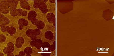
| This is an atomic force microscopy image of a graphene sheet draped over a Bacillus bacterium (left). The bacterium is about 1 micron or 1/25,000 of an inch wide. After applying vacuum and heat treatment, regular wrinkles form in the graphene (right, at twice the magnification). (Image: Vikas Berry, University of Illinois at Chicago) | |
| „The current across the graphene wrinkles is less than the current along them,” says Vikas Berry, associate professor and interim head of chemical engineering at UIC, who led the research. | |
| The key to formation of these wrinkles, he said, is graphene’s extreme flexibility at the nanometer scale, which allows formation of carbon nanotubes. | |
| „The wrinkle opens a ‘V’ in the electron cloud around each carbon atom,” Berry said, creating a dipole moment, which can open an electronic band gap that flat graphene does not have. | |
| Other researchers have created wrinkles in graphene by stretching the sheet and letting it snap back. But such wrinkles are not confined in microscale and cannot be directed towards a location on a micro-device, Berry said. | |
| He and his colleagues came up with a unique way to introduce circumscribed, guided, and regular graphene ripples using bacillus bacteria, by using the graphene itself as a check-valve to alter the volume of the cells. | |
| The researchers placed the bacteria in an electric field, causing them to line up like strings of hot dogs in repeating rows. Then they applied a sheet of graphene over the top. | |
| „Under vacuum, the graphene lifts, and lets water out,” Berry said. But under pressure, graphene sits back down on the substrate and prevents water from re-entering the bacteria, he said. | |
| „It’s a nanoscopic valve that actuates unidirectional fluid flow in a microorganism,” Berry said. „Futuristically, this valve operation could be applied to microfluidic devices where we want flow in one direction but not the other.” | |
| After the bacteria have been vacuum-shrunk, the graphene reconforms, but with wrinkles. After heat treatment, the resulting permanent ripples atop the bacteria are all aligned longitudinally, with a height of 7 to 10 nanometers, and a wavelength of about 32 nm. | |
| The wrinkles were observed by field emission scanning electron microscopy, which must be done under high vacuum, and by atomic force microscopy at atmospheric pressure. | |
| „The [ripple] wavelength is proportional to the thickness of the material, and graphene is the thinnest material in the world,” Berry said. „We envision that with graphene one could make the smallest wavelength wrinkles in the world – about 2 nanometers.” | |
| The next goal, he said, will be to create processes to further refine the ripples and vary their amplitude, wavelength and longitudinal length. | |
| To measure the effect of the ripples’ orientation on the carrier transport, graduate student Shikai Deng, the lead author of the paper, fabricated a plus-shaped device with bacteria aligned parallel to one pair of electrodes and perpendicular to another pair. He found the rippled graphene’s conduction barrier was greater in the transverse direction than in the longitudinal direction. | |
| The introduction of oriented ripples to graphene represents an entirely new material, Berry said. | |
| „Along with carbon nanotubes, graphene and fullerene, this is a new carbon allotrope – a half carbon nanotube linked to graphene,” he said. „The structure is different, and the fundamental electronic properties are new.” |
| Source: University of Illinois at Chicago |
Read more: Germs add ripples to make ‘groovy’ graphene
au creat cu succes un compus chimic sau o ansamblu cristalin, care repetă în mod autonom flipping sub lumină albastră .Echipa a făcut cristale compuse dintr-un compus organic, numit azobenzen, utilizat în mod obișnuit în fabricarea vopselelor, și acidul oleic, care se găsește în ulei de gătit. Moleculele azobenzenului au două forme diferite, structurale: cis și trans. Se convertesc repetat de la o formă la alta sub dreapta albastră.
| Posted: Jul 06, 2016 | |
On the path toward molecular robots(Nanowerk News) Researchers are working on mimicking cellular systems to develop molecular motors that can move or even deliver drugs to target tissues. Engineering such motors may ultimately lead to molecular robots that can execute more complex tasks. To this end, researchers must find ways to convert motion at the molecular level to motion at the macroscopic level. They also must find ways to cause chemical reactions to repeat autonomously and continuously. |
|
| Yoshiyuki Kageyama, Sadamu Takeda and colleagues at Hokkaido University’s Department of Chemistry have successfully created a chemical compound, or a crystalline assembly, which autonomously repeated flipping under blue light (Angewandte Chemie International Edition, „Dissipative and Autonomous Square-Wave Self-Oscillation of a Macroscopic Hybrid Self-Assembly under Continuous Light Irradiation”). | |
![]() |
|
| Schematic illustration of each step of the self-oscillatory motion. | |
| The team made crystals composed of an organic compound, called azobenzene, commonly used in dye manufacturing, and oleic acid, commonly found in cooking oil. Azobenzene molecules take two structurally different forms: cis and trans. They repetitively convert from one form to the other under blue right. The scientists tested if this would influence the structure of the azobenzene-oleic acid crystal, which contained unequal amounts of cis- and trans-azobenzene. | |
| By applying blue light to the crystals in solution, the team observed, under a microscope, an oscillatory bending-unbending motion of the thin crystals, suggesting the existence of two stable structures, bent or unbent, depending on the cis/trans ratio. The frequency of the motion increased when the light intensity was increased. Some crystal complexes even exhibited ‘swimming-like’ motions in the water. | |
| Previously reported light-responsive materials have been limited in their ability to deform. The properties of the compounds in the Hokkaido University-developed crystals, however, allowed for a two-step switching mechanism, resulting in regular repetitive oscillations. |
| Source: Hokkaido University |
Read more: On the path toward molecular robots