Generarea de materiale magnetice personalizate(Generation of tailored magnetic materials)

fizicienii sunt interesați de o generație de materiale artificiale, ale căror proprietăți pot fi controlate. Cercetătorii de la Universitatea din Geneva (UNIGE), Elveția, în colaborare cu echipele franceze și engleze, au reușit să manipuleze proprietățile a doi oxizi care alcătuiesc materialul artificial, mai exact au reușit să modifice proprietățile magnetice care pot fi fie feromagnetice sau antiferomagnetic; adică, cu sau fără moment magnetic net.

Posted: Apr 15, 2016

Generation of tailored magnetic materials

(Nanowerk News) Every day, new technologies require more precision in the intrinsic properties of the materials used. To meet increasingly specific requirements, physicists are interested in a generation of artificial materials, the properties of which can be controlled. Researchers at the University of Geneva (UNIGE), Switzerland, in collaboration with French and English teams, have succeed in manipulating the properties of two oxides which make up the artificial material, more exactly they managed to modify the magnetic properties which can be either ferromagnetic or antiferromagnetic; that is, with or without net magnetic moment.

The scientists have demonstrated, in their study published in Nature Communications („Interlayer coupling through a dimensionality-induced magnetic state”), that they are able now to control the magnetism in this type of materials and that they could, in the near future, offer tailored materials for the devices of tomorrow.
text
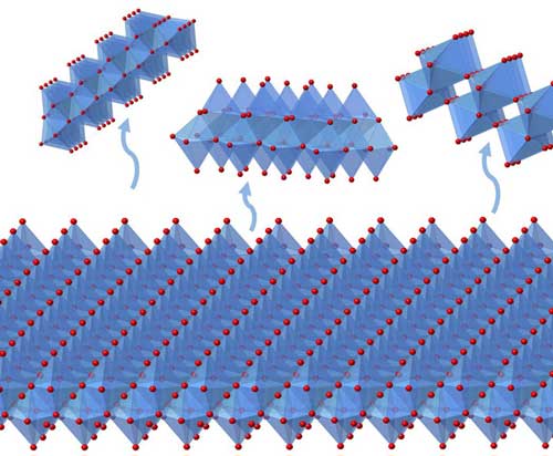
Artist view of the manipulation of the magnetic properties achieved in the oxide materials LaNiO3and LaMnO3 when few atomic layers of each material are grown one on top of the other successively. In this case, LaNiO3, which initially was conducting and non-magnetic, is found to become insulating and magnetic when in contact with LaMnO3. (Image: Marta Gibert Gutierrez – UNIGE)
When two materials are in contact, they interact in different ways and, sometimes, exchange electrons. But what happens when one stacks up ultrathin layers, of the order of one nanometer? «We have combined two materials, LaNiO3, a metallic paramagnet (without magnetic order), and LaMnO3, an insulating antiferromagnet, by alternating a layer of the first, then of the second, etc. We then observed what the influence of interactions at the interfaces was and we noticed a profound change in the intrinsic properties of the two materials», said a statement from Jean-Marc Triscone, professor at the Department of quantum matter physics in the Faculty of Science of UNIGE.
LaNiO3 and LaMnO3 have the same cubic crystalline structure, and thus the researchers can stack the elemental unit cells of these compounds, that is the small „cubes” made of just a few atoms, by using state-of-the-art technology. They then manage to create an artificial structure with a perfect alignment of the unit cells. To do this, the physicists deposit one unit cell after the other on a substrate; that is a small heated crystal tile. The layers are very thin and their thickness of about a nanometer is controlled precisely at the unit cell.
Goldsmith precision
«In order to realise a perfect structure on the crystal tile, we had to find the exact temperature and pressure conditions required to grow the materials one on top of the other. Then we investigated the properties of the interfaces depending on the number of layers stacked», explain Marta Gibert, researcher in physics at UNIGE and first author of the study. «Measurements of the physical properties then revealed that the properties of LaNiO3 are very different when in contact with LaMnO3. From being a metal without magnetic order, it becomes not only magnetic but also insulating. Moreover, the overall properties of the artificial material depend on the individual thickness of the layer of each material and they can also change as a function of the chosen thickness», added the physicist.
Thanks to this discovery, the researchers are therefore able to control the magnetic state of these materials – a track to build artificial tailored materials according to specific needs in the future. Such control of the magnetic interactions could especially be used to develop future magnetic memories, allowing the high dissipation energy of current processors to be reduced.
This research is not limited to magnetic materials, but it is also of interest for materials that are simultaneously magnetic and ferroelectric, another way to new memories or even to superconducting materials working at higher temperatures – a dream which may be not so distant.
Source: Université de Genève

Oamenii de știință dezvoltă un material bazat pe oxid de hafniu pentru un nou tip de memorie nevolatilă(Scientists grow a material based on hafnium oxide for a new type of non-volatile memory)

Oamenii de stiinta de la MIPT au reusit sa dezvolte pelicule feroelectrice ultra-subtiri (2,5 nanometri) pe baza de oxid de hafniu care ar putea fi folosite pentru a dezvolta elemente de memorie nevolatile numite jonctiuni tunel feroelectrice.

Posted: Apr 14, 2016

Scientists grow a material based on hafnium oxide for a new type of non-volatile memory

(Nanowerk News) Scientists from MIPT have succeeded in growing ultra-thin (2.5-nanometre) ferroelectric films based on hafnium oxide that could potentially be used to develop non-volatile memory elements called ferroelectric tunnel junctions. The results of the study have been published in the journal ACS Applied Materials & Interfaces („Ultrathin Hf0.5Zr0.5O2 Ferroelectric Films on Si”).

Function of a silicon-based ferroelectric tunnel junction
Function of a silicon-based ferroelectric tunnel junction. Information is written by applying an external electric field, which changes the direction of the ferroelectric’s polarization vector, and this in turn changes the shape of the potential barrier. Information is read by measuring the tunnel current, which depends on the shape of the barrier. (Image courtesy of the authors of the study)
Humans are constantly expanding the volume of stored and processed information, which according to statistics is doubling every 1.5 years. To store this information, we need increasing amounts of computer memory, especially non-volatile memory, which stores information even in the event of a power outage. Scientists all over the world are trying to develop faster and more compact storage devices. The ideal would be a “universal” memory device with the speed of RAM, the capacity of a hard drive, and the non-volatility of a flash drive.
There are many known principles that can be used to build memory, but each one has its drawbacks. This is why modern computers and mobile devices have multiple types of memory.
Non-volatile memory based on ferroelectric tunnel junctions is a promising development that has not yet been fully implemented. A ferroelectric is a material that is able to “remember” the direction of an externally applied electric field by the residual polarization charge.
Thin-film ferroelectrics have for a long time been used to make non-volatile memory devices, however it is extremely difficult to miniaturize them and, in addition to this, they are made of materials that are “incompatible” with the production processes used in modern microelectronics.
About ten years ago, after ferroelectric properties were demonstrated in ultra-thin single-crystal films of perovskites, an alternative concept for memory devices was proposed – based on the use of the tunnel effect.
Ferroelectrics are generally insulators and do not conduct electricity. However, if the ferroelectric layer is very thin, electrons can “slip” through with a certain probability, thanks to the quantum tunnelling effect. The probability of tunnelling depends on the size and shape of the potential barrier (the energy characteristics of the structure), and the electrons that “pass through” create a tunnel current.
The movement of the electrons in this case is similar to an obstacle course race, and the size of the obstacle is determined by the direction of the polarization vector, which alters the shape of the potential barrier (see image below). Information is written by applying a voltage to the electrodes next to the ultra-thin ferroelectric, and it is read by measuring the tunnelling current.
In theory, this type of memory may have an extremely high density, fast reading and writing speeds, and a low level of power consumption. It could become a non-volatile alternative to DRAM (dynamic random-access memory). Modern DRAM has a short retention time (approximately 0.1 seconds), after which the data is either lost or overwritten. Using this type of memory requires a large amount of power. Memory based on ferroelectric tunnel junctions will be able to save power, which is especially important for portable devices that run on batteries. However, until now, all prototypes of devices based on conventional ferroelectrics have not been compatible with silicon technology, which is used in the production of most modern chips.
The team of researchers from MIPT’s Laboratory of Functional Materials and Devices for Nanoelectronic, with the participation of their colleagues from the University of Nebraska (USA) and the University of Lausanne (Switzerland), have for the first time experimentally demonstrated that polycrystalline fused films of hafnium and zirconium oxides with a thickness of just 2.5 nm (see image below) retain their ferroelectric properties.
Hafnium oxide is already used in the production of modern silicon logic chips, and a few years ago ferroelectric properties were discovered in one of its modifications. In their study, the scientists from MIPT succeeded in growing an ultra-thin, tunnel-transparent film of this material on a silicon substrate, while maintaining the ferroelectric properties.
a polycrystalline fused film of hafnium and zirconium oxides grown on a highly doped Si substrate
Cross section of the structure developed: a polycrystalline fused film of hafnium and zirconium oxides grown on a highly doped Si substrate (upper electrode – titanium nitride) (Image courtesy of the authors of the study)
It is important to note that the method of atomic layer deposition (ALD) was used to grow the film. This technique is widely used today in the production of modern microprocessors and one of its particular benefits is that it enables functional layers to be grown in three-dimensional structures.
“Since the structures of this material are compatible with silicon technology, we can expect that new non-volatile memory devices with ferroelectric polycrystalline layers of hafnium oxide will be able to be built directly onto silicon in the near future,” says the corresponding author of the study and head of the Laboratory of Functional Materials and Devices for Nanoelectronics, Andrei Zenkevich.
Furthermore, if ferroelectric tunnel junctions based on hafnium oxide are developed, it can be hoped that they will be able to demonstrate memristor properties. This is a prerequisite for creating electronic synapses, which could be used in neuromorphic systems that are currently being developed. These systems have a fundamentally different computing architecture that simulates the functioning principles of the human brain.
Source: Moscow Institute of Physics and Technology

Noile nanoparticule luminoase transparente asigură protecție la temperaturi ridicate împotriva contrafacerii(New transparent luminous nanoparticles provide high temperature stable protection against counterfeiting)

au dezvoltat particule luminoase care pot rezista la temperaturi ridicate;Utilizând pigmenți luminoși din oxid de ytriu sau oxid de gadoliniu, desenele tipărite sunt create în alb sau transparent, care strălucesc roșu portocaliu în lumină UV sau raze

New transparent

Utilizarea nanotuburilor pentru a crea fotoni singulari pentru comunicarea cuantică(Using nanotubes to create single photons for quantum communication)

Cercetatorii au demonstrat un material nou, realizat din tuburi mici de carbon, care emite fotonii doriti la temperatura camerei.
Ascultarea electronică ar putea fi împiedicată prin codarea biților de informații în proprietățile sau stările mecanice cuantice ale fotonilor singuri. Fotoanele singulare emise de nanotuburi de carbon modificate sau dopate cu oxigen sunt deosebit de atractive pentru realizarea acestei tehnologii cuantice a informației.
Generarea de fotoni unici necesită un sistem izolat, mecanic cuantic, cu două nivele, care poate emite un singur foton într-un singur ciclu de emisie-excitație. În timp ce materialele nanometrice artificiale (cum ar fi punctele cuantice și centrele vacante în diamante) au fost explorate pentru generarea unui singur foton, nici unul nu a apărut ca un candidat ideal care să îndeplinească toate cerințele tehnologice.Dincolo de punerea în aplicare a acestei noi metode în tehnologiile de comunicare cuantică, sursele fotonice bazate pe nanotuburi ar putea permite alte tehnologii cuantice transformante, inclusiv măsurători de absorbție ultra-sensibile, imagini sub-difracție și computerizare liniară cuantică.

Posted: Apr 12, 2016

Using nanotubes to create single photons for quantum communication

(Nanowerk News) Critical information, ranging from credit card numbers to national security data, is sent in streams of light, or laser pulses. However, the data transmitted in this manner can be stolen by splitting out a few photons (packets of light) from the laser pulse. Such eavesdropping could be prevented by encoding the data into single photons. But that requires generating single photons. Researchers demonstrated a new material, made from tiny carbon tubes, that emits the desired photons at room temperature.

Digital eavesdropping could be prevented by encoding bits of information in the properties, or quantum mechanical states, of single photons. Single photons emitted by carbon nanotubes altered, or doped with oxygen, are especially attractive for realizing this quantum information technology.
Single photon generation requires an isolated, quantum mechanical, two-level system that can emit only one photon in one excitation-emission cycle. While artificial nanoscale materials (such as quantum dots and vacancy centers in diamonds) have been explored for single photon generation, none have emerged as the ideal candidate that meets all of the technological requirements.
These requirements include the ability to generate single photons in the 1.3 to 1.5 µm fiber optic telecommunication wavelength range at room temperature. Earlier studies revealed that carbon nanotubes were not suited for use in quantum communications because the tubes required extremely low temperatures and had strong photoluminescence fluctuations.
The deposition of a silicon dioxide layer (yellow layer) on a carbon nanotube (gray spheres) introduces solitary oxygen dopants (red spheres)
The deposition of a silicon dioxide layer (yellow layer) on a carbon nanotube (gray spheres) introduces solitary oxygen dopants (red spheres). A single photon (red and white star) is emitted when a dopant is excited by a laser pulse (green arrow). (Image courtesy of the Center for Integrated Nanotechnologies)
In contrast to these earlier findings, researchers led by Han Htoon and Stephen Doorn of the Center for Integrated Nanotechnologies showed that oxygen doping of carbon nanotubes can lead to fluctuation-free photoluminescence emission in the telecommunication wavelength range (Nature Nanotechnology, „Room-temperature single-photon generation from solitary dopants of carbon nanotubes”).
Experiments measuring the time-distribution of two successive photon emission events also unambiguously demonstrated single photon emission at room temperature. Furthermore, because oxygen doping is achieved through a simple deposition of a silicon dioxide layer, these doped carbon nanotubes are fully compatible with silicon microfabrication technology and can be fabricated into electrically driven single photon sources.
In addition, the silicon dioxide layer encapsulating the nanotubes allows for their easy integration into electronic and photonic integrated circuits.
Beyond the implementation of this new method into quantum communication technologies, nanotube-based single photon sources could enable other transformative quantum technologies, including ultra-sensitive absorption measurements, sub-diffraction imaging, and linear quantum computing.
Source: Department of Energy, Office of Science

Servirea nanopachetelor MoO3 proaspete, curate și monostrat subțiri ( Serving up fresh, clean, and monolayer-thin MoO3 nanosheets )

Molibden (α-MoO 3 ) conține , de asemenea , astfel de straturi 2D, care sunt legate între ele prin slabe forțe van der Waals care cauzeaza o molecula care urmeaza sa fie atras sau impins departe de o altă moleculă.
Structura unică stratată face ca α-MoO 3 să fie un material atrăgător pentru utilizarea în bateriile litiu-ion și dispozitivele electrochromice, cum ar fi ferestrele „inteligente” care controlează absorbția luminii solare în clădiri și oglinzile retrovizoare auto-dim care protejează șoferii de lumini de mare viteză .

Posted: Apr 09, 2016

Serving up fresh, clean, and monolayer-thin MoO3 nanosheets

(Nanowerk News) The 2010 Nobel Prize in physics was awarded to Manchester scientists Andre Geim and Konstantin Novoselov for their pioneering work with graphene, a 1-atom-thick, two-dimensional (2D) network of carbon that may revolutionize computing and electronics. Molybdenum trioxide (α-MoO3) also contains such 2D layers, which are linked together through weak van der Waals forces that cause a molecule to become attracted or pushed away from another molecule.

The unique layered-structure makes α-MoO3 an attractive material for use in lithium ion batteries and electrochromic devices, such as „smart” windows that control solar light absorption in buildings and auto-dim rearview mirrors that protect drivers from high-beam lights.
Schematic representation of the re-evaporation of ?-MoO<span class='subscript' style=3 molecular fragments from the surface of a single monolayer during film growth” border=”0″ align=”middle”>
Schematic representation of the re-evaporation of α-MoO3 molecular fragments from the surface of a single monolayer during film growth. At the optimum substrate temperature, only one monolayer “sticks” to the substrate because of strong interaction between the two; all other monolayers desorb because of weak van der Waals interaction with the first layer.
Results
Materials scientists at Pacific Northwest National Laboratory have overcome a set of challenges in synthesis and isolation of ultra-thin α-MoO3 layers. They developed a reproducible method for growing α-MoO3 sheets down to a monolayer in thickness. They used a thin-film deposition technique, molecular beam epitaxy (MBE), to synthesize α-MoO3. A stable oxide substrate provided the needed template (Nanoscale, „Iso-oriented Monolayer α-MoO3(010) Films Epitaxially Grown on SrTiO3(001)”).
The secret to growing monolayer-thin α-MoO3 is multi-faceted. The scientists’ success hinged on the right substrate that provides lateral confinement to the α-MoO3, and the carefully identified growth temperature, which allows α-MoO3 seeds to evolve, grow, but stop right at the monolayer thickness. Their results, which can greatly advance our current understanding on the material’s physical and chemical properties, appear in the scientific journal Nanoscale.
Why It Matters
Besides electrochemical and catalytic applications, ultra-thin α-MoO3 has also demonstrated its potential use in thin-film pseudocapacitors, light-emitting diodes, plasmon resonance generators, and biosensors. It is critical to be able to synthesis and isolate such 2D materials in a contamination-free environment (ultra-high vacuum) to better understand their intrinsic properties. The PNNL science team was able to meet these high standards by combining instrumentation and capabilities in the Environmental Molecular Sciences Laboratory (EMSL), a DOE national user facility.
Methods
„To grow the layers, we evaporate high-purity MoO3 powders held in a ceramic cup in ultra-high vacuum and put a substrate in front to collect the molecules,” said Dr. Yingge Du, lead scientist on the project. The evaporated MoO3 molecules will condense and form a well-ordered thin film on the heated substrate.
Du likens the substrate to a Lego© base plate. „If you throw atoms together randomly, they will stick together like a pile of Lego pieces in a random, messy way. But with a good base template, you can position the Legos in an ordered fashion, and make nice structures.”
And, MoO3 film growth is temperature sensitive. „At lower substrate temperatures, the material will grow as amorphous layers and become thicker and thicker. At higher temperatures, unwanted phases and structures start to evolve,” Du said. „We were extremely delighted that a very narrow temperature window was found for us to grow this material as a single monolayer.”
The correct temperature-in this case, 450°C-allows a crystalline layer to form on the substrate, stabilized by interfacial chemistry. However, the growth of subsequent MoO3 layers is suppressed by material re-evaporation from the substrate. The high substrate temperature and weak van der Waals bonding between adjacent MoO3 layers allow a self-limiting growth process, which provides a highly reliable technique for MoO3 to form and stay as a monolayer.
„Using traditional methods, these nanomaterials are hard to grow or isolate. The trick is to find the optimal temperature that not only provides enough thermal energy to start the crystal structure, but also is high enough to de-adsorb additional layers,” said Du.
What’s Next?
The research also paves the way to creating phase-pure, thicker films by lowering the growth temperature once the monolayer template is formed. The team plans to further investigate the electronic, transport, and catalytic properties of these films using various in situ spectroscopy and microscopy techniques at EMSL.
Source: Pacific Northwest National Laboratory

Read more: Serving up fresh, clean, and monolayer-thin MoO3 nanosheets

Punctele cuantice sporesc conversia de la lumină la curent în semiconductori din metal de tip dichalcogenid stratificat( Quantum dots enhance light-to-current conversion in layered metal dichalcogenide semiconductors)

Ideea de materiale stratificate bidimensionale«dopaj»cu puncte cuantice pentru a spori proprietățile de absorbție lumina lor arata promisiune pentru proiectarea de celule solare mai bune și fotodetectori

Posted: Apr 08, 2016

Quantum dots enhance light-to-current conversion in layered metal dichalcogenide semiconductors

(Nanowerk News) Harnessing the power of the sun and creating light-harvesting or light-sensing devices requires a material that both absorbs light efficiently and converts the energy to highly mobile electrical current. Finding the ideal mix of properties in a single material is a challenge, so scientists have been experimenting with ways to combine different materials to create „hybrids” with enhanced features.

In two just-published papers, scientists from the U.S. Department of Energy’s Brookhaven National Laboratory, Stony Brook University, and the University of Nebraska describe one such approach that combines the excellent light-harvesting properties of quantum dots with the tunable electrical conductivity of a layered tin disulfide semiconductor. The hybrid material exhibited enhanced light-harvesting properties through the absorption of light by the quantum dots and their energy transfer to tin disulfide, both in laboratory tests and when incorporated into electronic devices. The research paves the way for using these materials in optoelectronic applications such as energy-harvesting photovoltaics, light sensors, and light emitting diodes (LEDs).
Quantum Dots
Single nanocrystal spectroscopy identifies the interaction between zero-dimensional CdSe/ZnS nano crystals (quantum dots) and two-dimensional layered tin disulfide as a non-radiative energy transfer, whose strength increases with increasing number of tin disulfide layers. Such hybrid materials could be used in optoelectronic devices such as photovoltaic solar cells, light sensors, and LEDs. (click on image to enlarge)
According to Mircea Cotlet, the physical chemist who led this work at Brookhaven Lab’s Center for Functional Nanomaterials, a DOE Office of Science User Facility, „Two-dimensional metal dichalcogenides like tin disulfide have some promising properties for solar energy conversion and photodetector applications, including a high surface-to-volume aspect ratio. But no semiconducting material has it all. These materials are very thin and they are poor light absorbers. So we were trying to mix them with other nanomaterials like light-absorbing quantum dots to improve their performance through energy transfer.”
One paper, just published in the journal ACS Nano („Nonradiative Energy Transfer from Individual CdSe/ZnS Quantum Dots to Single-Layer and Few-Layer Tin Disulfide”), describes a fundamental study of the hybrid quantum dot/tin disulfide material by itself. The work analyzes how light excites the quantum dots (made of a cadmium selenide core surrounded by a zinc sulfide shell), which then transfer the absorbed energy to layers of nearby tin disulfide.
„We have come up with an interesting approach to discriminate energy transfer from charge transfer, two common types of interactions promoted by light in such hybrids,” said Prahlad Routh, a graduate student from Stony Brook University working with Cotlet and co-first author of the ACS Nano paper. „We do this using single nanocrystal spectroscopy to look at how individual quantum dots blink when interacting with sheet-like tin disulfide. This straightforward method can assess whether components in such semiconducting hybrids interact either by energy or by charge transfer.”
The researchers found that the rate for non-radiative energy transfer from individual quantum dots to tin disulfide increases with an increasing number of tin disulfide layers. But performance in laboratory tests isn’t enough to prove the merits of potential new materials. So the scientists incorporated the hybrid material into an electronic device, a photo-field-effect-transistor, a type of photon detector commonly used for light sensing applications.
As described in a paper published online March 24 in Applied Physics Letters („Hybrid quantum dot-tin disulfide field-effect transistors with improved photocurrent and spectral responsivity”), the hybrid material dramatically enhanced the performance of the photo-field-effect transistors—resulting in a photocurrent response (conversion of light to electric current) that was 500 percent better than transistors made with the tin disulfide material alone.
„This kind of energy transfer is a key process that enables photosynthesis in nature,” said Chang-Yong Nam, a materials scientist at Center for Functional Nanomaterials and co-corresponding author of the APL paper. „Researchers have been trying to emulate this principle in light-harvesting electrical devices, but it has been difficult particularly for new material systems such as the tin disulfide we studied. Our device demonstrates the performance benefits realized by using both energy transfer processes and new low-dimensional materials.”
Cotlet concludes, „The idea of ‘doping’ two-dimensional layered materials with quantum dots to enhance their light absorbing properties shows promise for designing better solar cells and photodetectors.”
Source: Brookhaven National Laboratory

Read more: Quantum dots enhance light-to-current conversion in layered metal dichalcogenide semiconductors

Oțelul de rupere a înregistrării ar putea fi folosit pentru armura corpului, scuturile pentru sateliți ( Recording-breaking steel could be used for body armor, shields for satellites

O echipă de ingineri a dezvoltat și testat un tip de oțel cu o abilitate de a rezista unui impact fără a se deforma permanent. Noul aliaj de oțel ar putea fi utilizat într-o gamă largă de aplicații, de la burghiu, la armura de corp pentru soldați, la carcasele rezistente la meteori pentru sateliți.

Posted: Apr 05, 2016

Recording-breaking steel could be used for body armor, shields for satellites

(Nanowerk News) A team of engineers has developed and tested a type of steel with a record-breaking ability to withstand an impact without deforming permanently. The new steel alloy could be used in a wide range of applications, from drill bits, to body armor for soldiers, to meteor-resistant casings for satellites.

The material is an amorphous steel alloy, a promising subclass of steel alloys made of arrangements of atoms that deviate from steel’s classical crystal-like structure, where iron atoms occupy specific locations.
Crystallinity in Steel alloy
This is a transmission electron microscopy image of different levels of crystallinity in the amorphous alloy. (Image: Jacobs School of Engineering/UC San Diego)
Researchers are increasingly looking to amorphous steel as a source of new materials that are affordable to manufacture, incredibly hard, but at the same time, not brittle. The researchers believe their work on the steel alloy, named SAM2X5-630, is the first to investigate how amorphous steels respond to shock.
SAM2X5-630 has the highest recorded elastic limit for any steel alloy, according to the researchers–essentially the highest threshold at which the material can withstand an impact without deforming permanently. The alloy can withstand pressure and stress of up to 12.5 giga-Pascals or about 125,000 atmospheres without undergoing permanent deformations.
The researchers, from the University of California, San Diego, the University of Southern California and the California Institute of Technology, describe the material’s fabrication and testing in a recent issue of Nature Scientific Reports („Shock Wave Response of Iron-based In Situ Metallic Glass Matrix Composites”).
„Because these materials are designed to withstand extreme conditions, you can process them under extreme conditions successfully,” said Olivia Graeve, a professor of mechanical engineering at the Jacobs School of Engineering at UC San Diego, who led the design and fabrication effort. Veronica Eliasson, an assistant professor at USC, led the testing efforts.
To make the solid materials that comprise the alloy, Graeve and her team mixed metal powders in a graphite mold. The powders were then pressurized at 100 mega-Pascals, or 1000 atmospheres, and exposed to a powerful current of 10,000 Ampers at 1165°F (630°C) during a process called spark plasma sintering.
The spark plasma sintering technique allows for enormous time and energy savings, Graeve said. „You can produce materials that normally take hours in an industrial setting in just a few minutes,” she said.
The process created small crystalline regions that are only a few nanometers in size, with hints of structure, which researchers believe are key to the material’s ability to withstand stress. This finding is promising because it shows that the properties of these types of metallic glasses can be fine-tuned to overcome shortcomings such as brittleness, which have prevented them from becoming commercially applicable on a large scale, Eliasson said.
Researchers at USC tested how the alloy responds to shock without undergoing permanent deformations by hitting samples of the material with copper plates fired from a gas gun at 500 to 1300 meters per second. The material did deform on impact, but not permanently.
The Hugoniot Elastic Limit (the maximum shock a material can take without irreversibly deforming) of a 1.5-1.8 mm-thick piece of SAM2X5-630 was measured at 11.76 ± 1.26 giga-Pascals.
By comparison, stainless steel has an elastic limit of 0.2 giga-Pascals, while that of tungsten carbide (a high-strength ceramic used in military armor) is 4.5 giga-Pascals. This isn’t to say that SAM2X5-630 has the highest elastic limit of any material known; diamonds top out at a whopping 60 giga-Pascals– they’re just not practical for many real-world applications. „The fact that the new materials performed so well under shock loading was very encouraging and should lead to plenty of future research opportunities,” said Eliasson.
The primary focus of future research efforts on these alloys is increasing the weight of the materials to make them more resistant to impacts.
Source: University of California – San Diego

Read more: Recording-breaking steel could be used for body armor, shields for satellites

Nanotuburile se aliniază pentru a forma filme

Filmele subțiri oferă posibilități de a realiza dispozitive flexibile electronice și fotonice (manipularea luminii)

Posted: Apr 04, 2016

Nanotubes line up to form films

(Nanowerk News) A simple filtration process helped Rice University researchers create flexible, wafer-scale films of highly aligned and closely packed carbon nanotubes.

Scientists at Rice, with support from Los Alamos National Laboratory, have made inch-wide films of densely packed, chirality-enriched single-walled carbon nanotubes through a process revealed today in Nature Nanotechnology („Wafer-scale monodomain films of spontaneously aligned single-walled carbon nanotubes”).
A scanning electron microscope image shows highly aligned and closely packed carbon nanotubes
A scanning electron microscope image shows highly aligned and closely packed carbon nanotubes gathered into a film by researchers at Rice University. (Image: Kono Lab/Rice University)
In the right solution of nanotubes and under the right conditions, the tubes assemble themselves by the millions into long rows that are aligned better than once thought possible, the researchers reported.
The thin films offer possibilities for making flexible electronic and photonic (light-manipulating) devices, said Rice physicist Junichiro Kono, whose lab led the study. Think of a bendable computer chip, rather than a brittle silicon one, and the potential becomes clear, he said.
„Once we have centimeter-sized crystals consisting of single-chirality nanotubes, that’s it,” Kono said. „That’s the holy grail for this field. For the last 20 years, people have been looking for this.”
The Rice lab is closing in, he said, but the films reported in the current paper are „chirality-enriched” rather than single-chirality. A carbon nanotube is a cylinder of graphene, with its atoms arranged in hexagons. How the hexagons are turned sets the tube’s chirality, and that determines its electronic properties. Some are semiconducting like silicon, and others are metallic conductors.
A film of perfectly aligned, single-chirality nanotubes would have specific electronic properties. Controlling the chirality would allow for tunable films, Kono said, but nanotubes grow in batches of random types.
highly aligned nanotube films
Rice University researchers discovered a method to make highly aligned nanotube films. The films may become valuable for flexible electronics and photonic devices. (Image: Jeff Fitlow/Rice University)
For now, the Rice researchers use a simple process developed at the National Institute of Standards and Technology to separate nanotubes by chirality. While not perfect, it was good enough to let the researchers make enriched films with nanotubes of different types and diameters and then make terahertz polarizers and electronic transistors.
The Rice lab discovered the filtration technique in late 2013 when graduate students and lead authors Xiaowei He and Weilu Gao inadvertently added a bit too much water to a nanotube-surfactant suspension before feeding it through a filter assisted by vacuum. (Surfactants keep nanotubes in a solution from clumping.)
The film that formed on the paper filter bore further investigation. „Weilu checked the film with a scanning electron microscope and saw something strange,” He said. Rather than drop randomly onto the paper like pickup sticks, the nanotubes – millions of them – had come together in tight, aligned rows.
„That first picture gave us a clue we might have something totally different,” He said. A year and more than 100 films later, the students and their colleagues had refined their technique to make nanotube wafers up to an inch wide (limited only by the size of their equipment) and of any thickness, from a few to hundreds of nanometers.
Further experiments revealed that each element mattered: the type of filter paper, the vacuum pressure and the concentration of nanotubes and surfactant. Nanotubes of any chirality and diameter worked, but each required adjustments to the other elements to optimize the alignment.
The films can be separated from the paper and washed and dried for use, the researchers said.
They suspect multiwalled carbon nanotubes and non-carbon nanotubes like boron nitride would work as well.
Co-author Wade Adams, a senior faculty fellow at Rice who specializes in polymer science, said the discovery is a step forward in a long quest for aligned structures.
„They formed what is called a monodomain in liquid crystal technology, in which all the rigid molecules line up in the same direction,” Adams said. „It’s astonishing. (The late Rice Nobel laureate) Rick Smalley and I worked very hard for years to make a single crystal of nanotubes, but these students have actually done it in a way neither of us ever imagined.”
Why do the nanotubes line up? Kono said the team is still investigating the mechanics of nucleation – that is, how the first few nanotubes on the paper come together. „We think the nanotubes fall randomly at first, but they can still slide around on the paper,” he said. „Van der Waals force brings them together, and they naturally seek their lowest-energy state, which is in alignment.” Because the nanotubes vary in length, the researchers suspect the overhangs force other tubes to line up as they join the array.
The researchers found their completed films could be patterned with standard lithography techniques. That’s yet another plus for manufacturers, said Kono, who started hearing buzz about the discovery months before the paper’s release.
„I gave an invited talk about our work at a carbon nanotube conference, and many people are already trying to reproduce our results,” he said. „I got so much enthusiastic response right after my talk. Everybody asked for the recipe.”
Source: Rice University

Read more: Nanotubes line up to form films

Noutăți noi de sticlă metalică

Inginerii au creat un material nou cu o structură chimică neobișnuită care îl face incredibil de greu și totuși elastic.
Materialul poate rezista la impacturi grele fără a se deforma – chiar și atunci când este împins dincolo de limitele sale elastice, nu rupe, în schimb își păstrează cea mai mare parte a rezistenței sale inițiale. Acest lucru îl face posibil să fie util într-o varietate de aplicații, de la burghie la armura pentru soldați până la căptușeli rezistente la meteoriti pentru sateliți.

Posted: Apr 04, 2016

New metallic glass bounces (w/video)

(Nanowerk News) Engineers have created a new material with an unusual chemical structure that makes it incredibly hard and yet elastic.

The material can withstand heavy impacts without deforming – even when pushed beyond its elastic limits, it doesn’t fracture, instead retaining most of its original strength. That makes it potentially useful in a variety of applications from drill bits to body armor for soldiers to meteor-resistant casings for satellites.
In the journal Scientific Reports („Shock Wave Response of Iron-based In Situ Metallic Glass Matrix Composites”), researchers from USC; the University of California, San Diego; and Caltech announced the creation of the material, which was produced by heating a powdered iron composite up to exactly 630 degrees Centigrade (1166 degrees Faherenheit) and then rapidly cooling it.
Bulk Metallic Glass (left) and Steel (right)
„In particular, the fact that the new materials performed so well under shock loading was very encouraging and should lead to plenty of future research opportunities,” said Veronica Eliasson, lead author of the paper and assistant professor at the USC Viterbi School of Engineering.
Dubbed SAM2X5-630, the new material has the highest impact resistance of any „bulk metallic glass” – a class of artificially generated materials first discovered in the 1960s that possess disproportionate strength, resilience, and elasticity due to their unusual chemical structure.
Typical metals and metal alloys have an organized, crystalline structure at the atomic level. Bulk metal glasses (BMGs, for short) are formed when metal and metal alloys are subjected to extreme heat and then rapidly cooled – exciting their atoms into disorganized arrangements, and then freezing them there.
In general, BMGs tend to be strong, resist scratching, tough to fracture, and highly elastic. One commercially available zirconium-based BMG is pound-for-pound twice as strong as titanium.
„Thanks to Professor Eliasson’s expertise in shocks and high velocity testing, we were able to observe the remarkable elastic limit of this material at high velocities, a behavior which was not evident from conventional mechanical tests,” said Andrea Hodge, principle investigator of the project and professor at USC Viterbi.
What makes SAM2X5-630 special is that it’s not entirely a glass – just mostly. For some reason, the exact timing and temperatures used to create it leave just a few hints of structure here and there – which seems to be the key to its unique nature. The exact same iron composite heated and cooled slightly differently yields a completely random atomic arrangement that lacks the impressive elastic properties.
„It has almost no internal structure, like glass, but you see tiny regions of crystallization,” Eliasson said. „We have no idea why a small amount of crystalline regions in these bulk metallic glasses makes such a big difference under shock loading.”
The Hugoniot Elastic Limit (the maximum shock it can take without irreversibly deforming) of a 1.5-1.8 mm-thick piece of SAM2X5-630 was measured at 11.76 ± 1.26 GPa.
For reference, stainless steel has an elastic limit of 0.2 GPa, while that of tungsten carbide (a high-strength ceramic used in military armor) is 4.5 GPa. This isn’t to say that SAM2X5-630 has the highest elastic limit of any material known; diamonds top out at a whopping 60 GPa, they’re just not practical for many real-world applications.
The material was produced at UC San Diego using a spark-plasma sintering process in which the iron compound is powdered, placed in a dye, and then zapped with a current – superheating it to the point of binding without ever liquefying it.
Eliasson and Hodge collaborated with former PhD student Gauri Khanolkar of USC, Michael Rauls of Caltech, and James Kelly and Olivia Graeve of the Jacobs School of Engineering at UC San Diego.
Source: University of Southern California

Read more: New metallic glass bounces (w/video)

Rametele de nanotuburi Ruthenium deschid ușile pentru catalizatori mai buni

Procesul implică două etape, creștere și gravură. Practic, hcp ruteniu nu cresc în mod natural într-o structură cristalină a poate fi făcută într-un cadru nano. Deci, echipa de creștere direcționată ruteniu pe o sămânță de paladiu cu structura fcc, pe care ruteniu replicat. Apoi au îndepărtat miezul de paladiu, lăsând în urmă la fcc cadru ruteniu nano.
Pentru a asigura materialul a avut un potențial catalizator, echipa a fugit cadrele ruteniu nano prin mai multe teste de diagnostic: reducerea p-nitrofenol prin NaBH4 și dehidrogenarea boran amoniac. In timp ce este nevoie de mai multe date pentru a cuantifica cât de bine ruteniu deține împotriva catalizatorilor metalici existente, Xia spune ca rezultatele din experimentele lor sunt promițătoare.

Posted: Apr 01, 2016

Ruthenium nanoframes open the doors to better catalysts

(Nanowerk News) The world is run by catalysts. They clean up after cars, help make fertilizers, and could be the key to better hydrogen fuel. Now, a team of chemists, led by Xiaohu Xia from Michigan Technological University, has found a better way to make metal nanoframe catalysts.

Last week, Nano Letters („Ru Nanoframes with an fcc Structure and Enhanced Catalytic Properties”) published the team’s study, which covers how the researchers made a catalyst for the first time out of the noble metal ruthenium.
Ruthenium Nanoframe
Using a two-part process, chemist Xiaohu Xia and his team found a way to turn ruthenium into a nanoframe, a promising metal catalyst. (Image: Michigan Tech, Xiaohu Xia)
The effort brought together a team from Michigan Tech, the Argonne National Laboratory, University of Texas at Dallas, and Temple University. The team’s break-through is not limited to ruthenium, however. Xia says the process they developed is most important.
„We are fine-tuning the surface, size, shape and crystal structure,” he says. „Our goal is to increase their catalytic activity while reducing the usage of this precious material.”
The key is more surface area. Nanoframes, which are nanoparticles with open centers, have an advantage with their gazebo-like atomic arrangements.
Xia adds that not only shape but crystal structure is important, „Because catalytic reactions occur only on the surface of materials, the surface atom arrangement has a great impact on determining the catalytic activity.”
In general, ruthenium nanocrystals adopt the hexagonal close-packed (hcp) structure. But Xia and his team came up with an elegant solution for making ruthenium nanocrystals with another structure: face-centered cubic (fcc) structure.
The process involves two steps, growth and etching. Basically, hcp ruthenium doesn’t naturally grow in a crystal structure that can be made into a nanoframe. So, the team directed ruthenium growth on a palladium seed with an fcc structure, which the ruthenium replicated. Then they removed the palladium core, leaving behind an fcc ruthenium nanoframe.
To ensure the material had catalytic potential, the team ran the ruthenium nanoframes through several diagnostic tests: the reduction of p-nitrophenol by NaBH4 and the dehydrogenation of ammonia borane. While more data is needed to quantify how well ruthenium holds up against existing metal catalysts, Xia says the results from their experiments are promising.
Once the material has been vetted, researchers will be able to start applying the catalyst to several big challenges. Namely, Xia says that ruthenium nanoframes and other catalysts with unique crystal structures could improve hydrogen fuel production and carbon storage.
Source: Michigan Technological University

Read more: Ruthenium nanoframes open the doors to better catalysts

Flat bor este un superconductor

Atomii de bor pot face mai mult decât un model atunci când se întâlnesc împreună ca material 2-D .Borul plat din punct de vedere atomic este metalic si își pierde rezistivitatea doar atunci când este foarte rece .

Posted: Mar 31, 2016

Flat boron is a superconductor

(Nanowerk News) Rice University scientists have determined that two-dimensional boron is a natural low-temperature superconductor. In fact, it may be the only 2-D material with such potential.

Rice theoretical physicist Boris Yakobson and his co-workers published their calculations that show atomically flat boron is metallic and will transmit electrons with no resistance. The work appears this month in the American Chemical Society journal Nano Letters („Can Two-Dimensional Boron Superconduct?”).
Electrons with opposite momenta and spins pair up via lattice vibrations
Electrons with opposite momenta and spins pair up via lattice vibrations at low temperatures in two-dimensional boron and give it superconducting properties, according to new research by theoretical physicists at Rice University. (Image: Evgeni Penev/Rice University)
The hitch, as with most superconducting materials, is that it loses its resistivity only when very cold, in this case between 10 and 20 kelvins (roughly, minus-430 degrees Fahrenheit). But for making very small superconducting circuits, it might be the only game in town.
The basic phenomenon of superconductivity has been known for more than 100 years, said Evgeni Penev, a research scientist in the Yakobson group, but had not been tested for its presence in atomically flat boron.
„It’s well-known that the material is pretty light because the atomic mass is small,” Penev said. „If it’s metallic too, these are two major prerequisites for superconductivity. That means at low temperatures, electrons can pair up in a kind of dance in the crystal.”
„Lower dimensionality is also helpful,” Yakobson said. „It may be the only, or one of very few, two-dimensional metals. So there are three factors that gave the initial motivation for us to pursue the research. Then we just got more and more excited as we got into it.”
Electrons with opposite momenta and spins effectively become Cooper pairs; they attract each other at low temperatures with the help of lattice vibrations, the so-called „phonons,” and give the material its superconducting properties, Penev said. „Superconductivity becomes a manifestation of the macroscopic wave function that describes the whole sample. It’s an amazing phenomenon,” he said.
It wasn’t entirely by chance that the first theoretical paper establishing conductivity in a 2-D material appeared at roughly the same time the first samples of the material were made by laboratories in the United States and China. In fact, an earlier paper by the Yakobson group had offered a road map for doing so.
That 2-D boron has now been produced is a good thing, according to Yakobson and lead authors Penev and Alex Kutana, a postdoctoral researcher at Rice. „We’ve been working to characterize boron for years, from cage clusters to nanotubes to planer sheets, but the fact that these papers appeared so close together means these labs can now test our theories,” Yakobson said.
„In principle, this work could have been done three years ago as well,” he said. „So why didn’t we? Because the material remained hypothetical; okay, theoretically possible, but we didn’t have a good reason to carry it too far.
„But then last fall it became clear from professional meetings and interactions that it can be made. Now those papers are published. When you think it’s coming for real, the next level of exploration becomes more justifiable,” Yakobson said.
Boron atoms can make more than one pattern when coming together as a 2-D material, another characteristic predicted by Yakobson and his team that has now come to fruition. These patterns, known as polymorphs, may allow researchers to tune the material’s conductivity „just by picking a selective arrangement of the hexagonal holes,” Penev said.
He also noted boron’s qualities were hinted at when researchers discovered more than a decade ago that magnesium diborite is a high-temperature electron-phonon superconductor. „People realized a long time ago the superconductivity is due to the boron layer,” Penev said. „The magnesium acts to dope the material by spilling some electrons into the boron layer. In this case, we don’t need them because the 2-D boron is already metallic.”
Penev suggested that isolating 2-D boron between layers of inert hexagonal boron nitride (aka „white graphene”) might help stabilize its superconducting nature.
Without the availability of a block of time on several large government supercomputers, the study would have taken a lot longer, Yakobson said. „Alex did the heavy lifting on the computational work,” he said. „To turn it from a lunchtime discussion into a real quantitative research result took a very big effort.”
The paper is the first by Yakobson’s group on the topic of superconductivity, though Penev is a published author on the subject. „I started working on superconductivity in 1993, but it was always kind of a hobby, and I hadn’t done anything on the topic in 10 years,” Penev said. „So this paper brings it full circle.”
Source: Rice University

Read more: Flat boron is a superconductor