Noi senzori de nanotehnologie ar putea permite fabricarea de textile mai inteligente(Novel nanotechnology sensors could enable smarter textiles)

O echipă de ingineri de la Universitatea din Delaware dezvoltă produse inteligente de generație următoare, prin crearea de straturi compozite de nanotuburi de carbon flexibile pe o gamă largă de fibre, inclusiv bumbac, nailon și lână.Nanotuburile de carbon conferă această capacitate impresionantă de detectare ușoară, flexibilă și respirabilă. Când materialul este stors, se măsoară cu ușurință modificări electrice mari ale materialului.

Posted: Aug 16, 2018

Novel nanotechnology sensors could enable smarter textiles

(Nanowerk News) A team of engineers at the University of Delaware is developing next-generation smart textiles by creating flexible carbon nanotube composite coatings on a wide range of fibers, including cotton, nylon and wool. Their discovery is reported in the journal ACS Sensors („Thin and Flexible Carbon Nanotube-Based Pressure Sensors with Ultrawide Sensing Range”) where they demonstrate the ability to measure an exceptionally wide range of pressure – from the light touch of a fingertip to being driven over by a forklift.

Fabric coated with this sensing technology could be used in future “smart garments” where the sensors are slipped into the soles of shoes or stitched into clothing for detecting human motion.
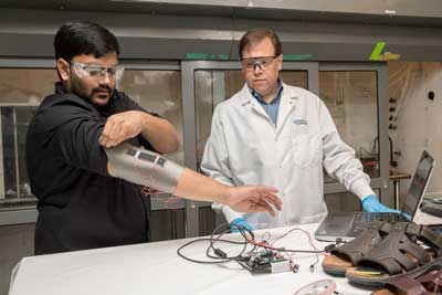
Sagar Doshi (left) and Erik Thostenson test an elbow sleeve outfitted with one of their novel sensors
Sagar Doshi (left) and Erik Thostenson test an elbow sleeve outfitted with one of their novel sensors. (Image: University of Delaware)
Carbon nanotubes give this light, flexible, breathable fabric coating impressive sensing capability. When the material is squeezed, large electrical changes in the fabric are easily measured.
“As a sensor, it’s very sensitive to forces ranging from touch to tons,” said Erik Thostenson, an associate professor in the Departments of Mechanical Engineering and Materials Science and Engineering.
Nerve-like electrically conductive nanocomposite coatings are created on the fibers using electrophoretic deposition (EPD) of polyethyleneimine functionalized carbon nanotubes.
“The films act much like a dye that adds electrical sensing functionality,” said Thostenson. “The EPD process developed in my lab creates this very uniform nanocomposite coating that is strongly bonded to the surface of the fiber. The process is industrially scalable for future applications.”
Now, researchers can add these sensors to fabric in a way that is superior to current methods for making smart textiles. Existing techniques, such as plating fibers with metal or knitting fiber and metal strands together, can decrease the comfort and durability of fabrics, said Thostenson, who directs UD’s Multifunctional Composites Laboratory.
The nanocomposite coating developed by Thostenson’s group is flexible and pleasant to the touch and has been tested on a range of natural and synthetic fibers, including Kevlar, wool, nylon, Spandex and polyester. The coatings are just 250 to 750 nanometers thick — about 0.25 to 0.75 percent as thick as a piece of paper — and would only add about a gram of weight to a typical shoe or garment. What’s more, the materials used to make the sensor coating are inexpensive and relatively eco-friendly, since they can be processed at room temperature with water as a solvent.

Exploring Future Applications

One potential application of the sensor-coated fabric is to measure forces on people’s feet as they walk. This data could help clinicians assess imbalances after injury or help to prevent injury in athletes. Specifically, Thostenson’s research group is collaborating with Jill Higginson, professor of mechanical engineering and director of the Neuromuscular Biomechanics Lab at UD, and her group as part of a pilot project funded by Delaware INBRE. Their goal is to see how these sensors, when embedded in footwear, compare to biomechanical lab techniques such as instrumented treadmills and motion capture.
During lab testing, people know they are being watched, but outside the lab, behavior may be different.
“One of our ideas is that we could utilize these novel textiles outside of a laboratory setting — walking down the street, at home, wherever,” said Thostenson.
Sagar Doshi, a doctoral student in mechanical engineering at UD, is the lead author on the paper. He worked on making the sensors, optimizing their sensitivity, testing their mechanical properties and integrating them into sandals and shoes. He has worn the sensors in preliminary tests, and so far, the sensors collect data that compares with that collected by a force plate, a laboratory device that typically costs thousands of dollars.
“Because the low-cost sensor is thin and flexible the possibility exists to create custom footwear and other garments with integrated electronics to store data during their day-to-day lives,” Doshi said. “This data could be analyzed later by researchers or therapists to assess performance and ultimately bring down the cost of healthcare.”
This technology could also be promising for sports medicine applications, post-surgical recovery, and for assessing movement disorders in pediatric populations.
“It can be challenging to collect movement data in children over a period of time and in a realistic context,” said Robert Akins, Director of the Center for Pediatric Clinical Research and Development at the Nemours – Alfred I. duPont Hospital for Children in Wilmington and affiliated professor of materials science and engineering, biomedical engineering and biological sciences at UD. “Thin, flexible, highly sensitive sensors like these could help physical therapists and doctors assess a child’s mobility remotely, meaning that clinicians could collect more data, and possibly better data, in a cost-effective way that requires fewer visits to the clinic than current methods do.”
Interdisciplinary collaboration is essential for the development of future applications, and at UD, engineers have a unique opportunity to work with faculty and students from the College of Health Sciences on UD’s Science, Technology and Advanced Research (STAR) Campus.
“As engineers, we develop new materials and sensors but we don’t always understand the key problems that doctors, physical therapists and patients are facing,” said Doshi. “We collaborate with them to work on the problems they are facing and either direct them to an existing solution or create an innovative solution to solve that problem.”
Thostenson’s research group also uses nanotube-based sensors for other applications, such as structural health monitoring.
“We’ve been working with carbon nanotubes and nanotube-based composite sensors for a long time,” said Thostenson, who is affiliated faculty at UD’s Center for Composite Materials (UD-CCM). Working with researchers in civil engineering his group has pioneered the development of flexible nanotube sensors to help detect cracks in bridges and other types of large-scale structures.
“One of the things that has always intrigued me about composites is that we design them at varying lengths of scale, all the way from the macroscopic part geometries, an airplane or an airplane wing or part of a car, to the fabric structure or fiber level. Then, the nanoscale reinforcements like carbon nanotubes and graphene give us another level to tailor the material structural and functional properties. Although our research may be fundamental, there is always an eye towards applications. UD-CCM has a long history of translating fundamental research discoveries in the laboratory to commercial products through UD-CCM’s industrial consortium.”
Source: University of Delaware

Proiectarea nanocristalelor pentru optoelectronica mai eficienta(Designing nanocrystals for more efficient optoelectronics)

Lucrările lor introduc o nouă clasă de sisteme nanocrystal-in-glass, care sporesc eficiența optoelectronicii, cum ar fi fotovoltaica și divizarea apelor induse de lumină.Această strategie va ajuta la proiectarea unor nanomateriale personalizate. Cercetătorii sugerează acum să utilizeze strategia prezentată pentru nanocompozitele semiconductoare relevante din punct de vedere tehnologic și sistemele nanoparticule în sticlă.

Posted: Aug 15, 2018

Designing nanocrystals for more efficient optoelectronics

(Nanowerk News) New artificial materials for semiconductors used in solar cells or photoelectrochemical cells that are designed from scratch with totally new and tailored properties: this is the latest research topic of Stefan Wippermann, head of the group “Atomistic Modelling“ at the Max-Planck-Institut für Eisenforschung), and his team. They characterized for the first time with atomic resolution a typical material system and are able to set design principles.

Their work introduces a new class of nanocrystal-in-glass systems, which increase the efficiency of optoelectronics such as photovoltaics and light-induced water splitting.
The Max Planck researchers published their latest findings in the journal Nature Nanotechnology(„Surface chemistry and buried interfaces in all-inorganic nanocrystalline solids”).
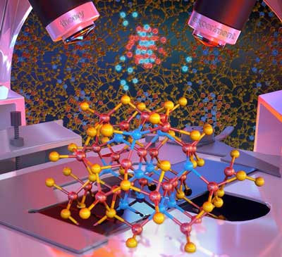
The luminescent atoms in the image show a nanocrystal which is characterized with atomistic resolution, including its interface chemistry
The luminescent atoms in the image show a nanocrystal which is characterized with atomistic resolution, including its interface chemistry. (Image: Peter Allen)
Nanocrystals can be used as “artificial atoms” to create designer materials for electronic applications and solar energy conversion as they are controllable, potentially non-toxic and earth-abundant. In collaboration with the groups of Dmitri Talapin and Giulia Galli, University of Chicago, wet-chemical techniques were used to synthesize those nanocrystals and assemble them into semiconducting nanocomposites.
“One great advantage of designing nanocrystals is that we are able to choose their properties”, explains Wippermann. “As we develop our own “atoms”, we do not rely anymore on the chemical properties of elements but are able to design materials with target properties through nanostructuring.”
That means the researchers can abstain for example from toxic or rare elements. And even though their current model system is still using toxic elements, they embed the nanocrystals into solid matrices so that the nanocrystals are not spread into air.
“The current key challenge is not the production of the nanocrystals themselves but rather the understanding and controlling of their interface chemistry and defects, as their surfaces and interfaces are only a few nanometres in size and buried inside the material”, says Wippermann.
He and his team produced and analysed buried interfaces in solids of indium arsenide nanoparticles capped with thiostannate (Sn2S64-) ligands as prototypical nanocomposites. The ligands are used during the synthesis of the nanocomposites. With the help of theoretical and experimental techniques they found that the ligands are not adsorbed as intact units but decompose upon contact with the nanocrystal surface, forming an amorphous matrix around the nanocrystals.
Exactly this matrix influences the electronic transport of the nanocrystal solids, as the decomposed ligands form a passivation layer on the nanocrystal surface and only on top of this layer an intact ligand may adsorb.
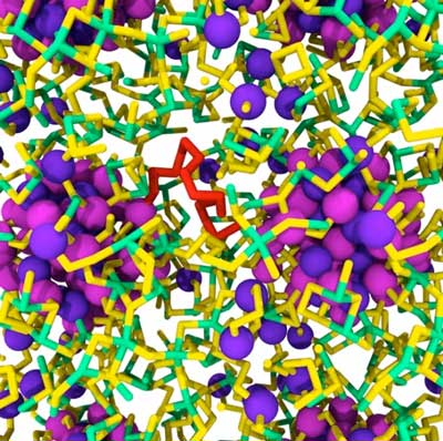
Indium arsenide nanocrystals embedded in amorphous SnS3
Indium arsenide nanocrystals embedded in amorphous SnS3. Magenta and violet balls, green and yellow tubes denote indium, arsenic, tin and sulphur atoms, respectively. A sulphur chain in red. (Image: Stefan Wippermann)
Another passivation mechanism is the incorporation of sulphur into the subsurface layer. Arsenic in turn diffuses into the matrix, leading to the formation of characteristic defects. These defects explain the observed switching between positive and negative photoconductivity. Simulations showed that the indium arsenide nanocrystals draw sulphur from the matrix leading to the formation of a sulphur shell around the nanocrystals.
Sulphur also affects the amount and character of defects in the nanocomposite: A high sulphur content reduces the number of dangling bond defects in the nanocomposite and leads to the formation of sulphur chains acting as hole-conducting interconnects between the nanocrystals.
The Max Planck scientists show that the properties of nanocrystal-based solids are influenced by the size, shape, composition, surface chemistry and mutual interactions of nanocrystals. The strong quantum confinement of charge carriers inside the nanocrystals enable efficient carrier multiplication, where a single high energy photon creates multiple electron-hole pairs, which contribute to the conductivity.
This way optoelectronics can be made more efficient. Nanocrystals capped with molecular metal chalcogenide complexes have especially high electron mobilities, which allow for fast extraction of the photogenerated charges. The scientists established a strategy to characterize buried interfaces in inorganic nanocomposites and more generally nanoparticle-in-glass systems.
This strategy will help in designing tailor-made nanomaterials. The researchers now suggests to employ the presented strategy to technologically relevant semiconductor nanocomposites and nanoparticle-in-glass systems.
Source: Max-Planck-Institut für Eisenforschung

Nanoparticulele magnetice trag ultimele picături de ulei din apele din puț(Magnetic nanoparticles pull last drops of oil from well water)

Laboratorul Rice al inginerului chimic Sibani, Lisa Biswal, a realizat un compus cu nanoparticule magnetice care separă eficient picăturile de țiței din apa produsă, care s-au dovedit dificil de îndepărtat prin metodele actuale.Nanoparticulele magnetice trag ultimele picături de ulei din apele din puț

Posted: Aug 15, 2018

Magnetic nanoparticles pull last drops of oil from well water

(Nanowerk News) Oil and water tend to separate, but they mix well enough to form stable oil-in-water emulsions in produced water from oil reservoirs to become a problem. Rice University scientists have developed a nanoparticle-based solution that reliably removes more than 99 percent of the emulsified oil that remains after other processing is done.

The Rice lab of chemical engineer Sibani Lisa Biswal made a magnetic nanoparticle compound that efficiently separates crude oil droplets from produced water that have proven difficult to remove with current methods.
The research is detailed in a paper in the Royal Society of Chemistry journal Environmental Science: Water Research & Technology („Recyclable amine-functionalized magnetic nanoparticles for efficient demulsification of crude oil-in-water emulsions”).
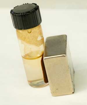
magnetic nanoparticles draw in the bulk of the oil and are then attracted to the magnet
Rice University engineers have developed magnetic nanoparticles that separate the last droplets of oil from produced water at wells. The particles draw in the bulk of the oil and are then attracted to the magnet, as demonstrated here. (Image:Jeff Fitlow)
Produced water comes from production wells along with oil. It often includes chemicals and surfactants pumped into a reservoir to push oil to the surface from tiny pores or cracks, either natural or fractured, deep underground. Under pressure and the presence of soapy surfactants, some of the oil and water form stable emulsions that cling together all the way back to the surface.
While methods exist to separate most of the oil from the production flow, engineers at Shell Global Solutions, which sponsored the project, told Biswal and her team that the last 5 percent of oil tends to remain stubbornly emulsified with little chance to be recovered.
“Injected chemicals and natural surfactants in crude oil can oftentimes chemically stabilize the oil-water interface, leading to small droplets of oil in water which are challenging to break up,” said Biswal, an associate professor of chemical and biomolecular engineering and of materials science and nanoengineering.
The Rice lab’s experience with magnetic particles and expertise in amines, courtesy of former postdoctoral researcher and lead author Qing Wang, led it to combine techniques. The researchers added amines to magnetic iron nanoparticles. Amines carry a positive charge that helps the nanoparticles find negatively charged oil droplets. Once they do, the nanoparticles bind the oil. Magnets are then able to pull the droplets and nanoparticles out of the solution.
“It’s often hard to design nanoparticles that don’t simply aggregate in the high salinities that are typically found in reservoir fluids, but these are quite stable in the produced water,” Biswal said.
The enhanced nanoparticles were tested on emulsions made in the lab with model oil as well as crude oil.
In both cases, researchers inserted nanoparticles into the emulsions, which they simply shook by hand and machine to break the oil-water bonds and create oil-nanoparticle bonds within minutes. Some of the oil floated to the top, while placing the test tube on a magnet pulled the infused nanotubes to the bottom, leaving clear water in between.
Best of all, Biswal said, the nanoparticles can be washed with a solvent and reused while the oil can be recovered. The researchers detailed six successful charge-discharge cycles of their compound and suspect it will remain effective for many more.
She said her lab is designing a flow-through reactor to process produced water in bulk and automatically recycle the nanoparticles. That would be valuable for industry and for sites like offshore oil rigs, where treated water could be returned to the ocean.
Source: Rice University

Cerneluri 3D care pot fi șterse selectiv(3D inks that can be erased selectively)

) Imprimarea 3D prin scrierea directă cu laser permite producerea de structuri cu dimensiuni micro-metrice pentru multe aplicații, de la biomedicină la microelectronică până la metamateriale optice. Cercetătorii de la Institutul de Tehnologie din Karlsruhe (KIT) au dezvoltat acum cerneluri 3D care pot fi șterse selectiv. Acest lucru permite degradarea și reasamblarea specifică a structurilor foarte precise pe micrometrele și pe scalele nanometrice.

Posted: Aug 14, 2018

3D inks that can be erased selectively

(Nanowerk News) 3D printing by direct laser writing enables production of micro-meter-sized structures for many applications, from biomedicine to microelectronics to optical metamaterials. Researchers of Karlsruhe Institute of Technology (KIT) have now developed 3D inks that can be erased selectively. This allows specific degradation and reassembly of highly precise structures on the micrometer and nanometer scales.

The new photoresists are presented in the journal Nature Communications („Adding chemically selective subtraction to multi-material 3D additive manufacturing”).
Three-dimensional microstructures made of various cleavable photoresists
Three-dimensional microstructures made of various cleavable photoresists. The scanning electron microscopies show the selective degradation of the structures (scaling 20 µm). (© Nature Communications) (click on image to enlarge)
3D printing is gaining importance, as it allows for the efficient manufacture of complex geometries. A very promising method is direct laser writing: a computer-controlled focused laser beam acts as a pen and produces the desired structure in a photoresist. In this way, three-dimensional structures with details in the sub-micrometer range can be produced.
“The high resolution is very attractive for applications requiring very precise filigree structures, such as in biomedicine, microfluidics, microelectronics or for optical metamaterials,” say Professor Christopher Barner-Kowollik, Head of the Macromolecular Architectures Group of KIT’s Institute for Chemical Technology and Polymer Chemistry (ITCP) and of the Soft Matter Materials Group of Queensland University of Technology (QUT) in Brisbane, Australia, and Dr. Eva Blasco of the ITCP of KIT.
Over a year ago, KIT researchers already succeeded in expanding the possibilities of direct laser writing: the working groups of Professor Martin Wegener at the Institute of Applied Physics (APH) and the Institute of Nanotechnology (INT) of KIT and of Professor Christopher Barner-Kowollik developed an erasable ink for 3D printing. Thanks to reversible binding, the building blocks of the ink can be separated again.
Now, the scientists from Karlsruhe and Brisbane have largely refined their development. As reported in the journal Nature Communications, they have developed several inks, in different colors so to speak, that can be erased independently of each other. This enables selective and sequential degradation and reassembly of the laser-written microstructures.
In case of highly complex constructions, for instance, temporary supports can be produced and removed again later on. It may also be possible to add or remove parts to or from three-dimensional scaffolds for cell growth, the objective being to observe how the cells react to such changes. Moreover, the specifically erasable 3D inks allow for the exchange of damaged or worn parts in complex structures.
When producing the cleavable photoresists, the researchers were inspired by degradable biomaterials. The photoresists are based on silane compounds that can be cleaved easily. Silanes are silicon-hydrogen compounds. The scientists used specific atom substitution for preparing the photoresists. In this way, microstructures can be degraded specifically under mild conditions without structures with other material properties being damaged.
This is the major advantage over formerly used erasable 3D inks. New photoresists also contain the monomer pentaerythritol triacrylate that significantly enhances writing without affecting cleavability.
Source: Karlsruhe Institute of Technology

Structura de carbon pe termen lung „schwarzite” se alătură grafenului, familiei fullerene(Long-sought carbon structure ‘schwarzite’ joins graphene, fullerene family)

chimiștii au demonstrat că trei structuri de carbon create recent de către oamenii de știință din Coreea de Sud și Japonia sunt, de fapt, schwarzi-urile căutate de mult timp, pe care cercetătorii le prezică că vor avea proprietăți electrice unice și de stocare cum ar fi cele descoperite acum în buckminsterfullerenes sau fullerene pentru scurt), nanotuburi și grafen.
Noile structuri au fost construite în interiorul porilor de zeoliți, forme cristaline de dioxid de siliciu – nisip – utilizat mai frecvent ca dedurizatori de apă în detergenții de rufe și pentru a crăpa catalitic petrolul în benzină. Denumit carbonul zeolit-template (ZTC), structurile au fost investigate pentru posibile proprietăți interesante, deși creatorii nu au fost conștienți de identitatea lor ca schwarzites, pe care chimistii teoretici au lucrat timp de decenii.

Posted: Aug 13, 2018

Long-sought carbon structure ‘schwarzite’ joins graphene, fullerene family

(Nanowerk News) The discovery of buckyballs surprised and delighted chemists in the 1980s, nanotubes jazzed physicists in the 1990s, and graphene charged up materials scientists in the 2000s, but one nanoscale carbon structure – a negatively curved surface called a schwarzite – has eluded everyone. Until now.

University of California, Berkeley, chemists have proved that three carbon structures recently created by scientists in South Korea and Japan are in fact the long-sought schwarzites, which researchers predict will have unique electrical and storage properties like those now being discovered in buckminsterfullerenes (buckyballs or fullerenes for short), nanotubes and graphene.
The new structures were built inside the pores of zeolites, crystalline forms of silicon dioxide – sand – more commonly used as water softeners in laundry detergents and to catalytically crack petroleum into gasoline. Called zeolite-templated carbons (ZTC), the structures were being investigated for possible interesting properties, though the creators were unaware of their identity as schwarzites, which theoretical chemists have worked on for decades.
Carbon atoms (black) assembling on the molecular surface of a zeolite (red oxygen atoms and yellow silicon atoms) to form a negatively curved schwarzite. (Graphics by Yongjin Lee and Efrem Braun)
Based on this theoretical work, chemists predict that schwarzites will have unique electronic, magnetic and optical properties that would make them useful as supercapacitors, battery electrodes and catalysts, and with large internal spaces ideal for gas storage and separation.
UC Berkeley postdoctoral fellow Efrem Braun and his colleagues identified these ZTC materials as schwarzites based of their negative curvature, and developed a way to predict which zeolites can be used to make schwarzites and which can’t.
“We now have the recipe for how to make these structures, which is important because, if we can make them, we can explore their behavior, which we are working hard to do now,” said Berend Smit, an adjunct professor of chemical and biomolecular engineering at UC Berkeley and an expert on porous materials such as zeolites and metal-organic frameworks.
Smit, the paper’s corresponding author, Braun and their colleagues in Switzerland, China, Germany, Italy and Russia will report their discovery this week in the journal Proceedings of the National Academy of Sciences („Generating carbon schwarzites via zeolite-templating „). Smit is also a faculty scientist at Lawrence Berkeley National Laboratory.

Playing with carbon

Diamond and graphite are well-known three-dimensional crystalline arrangements of pure carbon, but carbon atoms can also form two-dimensional “crystals” — hexagonal arrangements patterned like chicken wire. Graphene is one such arrangement: a flat sheet of carbon atoms that is not only the strongest material on Earth, but also has a high electrical conductivity that makes it a promising component of electronic devices.
schwarzite carbon cage
The cage structure of a schwarzite that was formed inside the pores of a zeolite. The zeolite is subsequently dissolved to release the new material. (Image: Yongjin Lee and Efrem Braun)
Graphene sheets can be wadded up to form soccer ball-shaped fullerenes – spherical carbon cages that can store molecules and are being used today to deliver drugs and genes into the body. Rolling graphene into a cylinder yields fullerenes called nanotubes, which are being explored today as highly conductive wires in electronics and storage vessels for gases like hydrogen and carbon dioxide. All of these are submicroscopic, 10,000 times smaller than the width of a human hair.
To date, however, only positively curved fullerenes and graphene, which has zero curvature, have been synthesized, feats rewarded by Nobel Prizes in 1996 and 2010, respectively.
In the 1880s, German physicist Hermann Schwarz investigated negatively curved structures that resemble soap-bubble surfaces, and when theoretical work on carbon cage molecules ramped up in the 1990s, Schwarz’s name became attached to the hypothetical negatively curved carbon sheets.
“The experimental validation of schwarzites thus completes the triumvirate of possible curvatures to graphene; positively curved, flat, and now negatively curved,” Braun added.

Minimize me

Like soap bubbles on wire frames, schwarzites are topologically minimal surfaces. When made inside a zeolite, a vapor of carbon-containing molecules is injected, allowing the carbon to assemble into a two-dimensional graphene-like sheet lining the walls of the pores in the zeolite. The surface is stretched tautly to minimize its area, which makes all the surfaces curve negatively, like a saddle. The zeolite is then dissolved, leaving behind the schwarzite.
soap bubble schwarzite structure
A computer-rendered negatively curved soap bubble that exhibits the geometry of a carbon schwarzite. (Image: Felix Knöppel)
“These negatively-curved carbons have been very hard to synthesize on their own, but it turns out that you can grow the carbon film catalytically at the surface of a zeolite,” Braun said. “But the schwarzites synthesized to date have been made by choosing zeolite templates through trial and error. We provide very simple instructions you can follow to rationally make schwarzites and we show that, by choosing the right zeolite, you can tune schwarzites to optimize the properties you want.”
Researchers should be able to pack unusually large amounts of electrical charge into schwarzites, which would make them better capacitors than conventional ones used today in electronics. Their large interior volume would also allow storage of atoms and molecules, which is also being explored with fullerenes and nanotubes. And their large surface area, equivalent to the surface areas of the zeolites they’re grown in, could make them as versatile as zeolites for catalyzing reactions in the petroleum and natural gas industries.
Braun modeled ZTC structures computationally using the known structures of zeolites, and worked with topological mathematician Senja Barthel of the École Polytechnique Fédérale de Lausanne in Sion, Switzerland, to determine which of the minimal surfaces the structures resembled.
The team determined that, of the approximately 200 zeolites created to date, only 15 can be used as a template to make schwarzites, and only three of them have been used to date to produce schwarzite ZTCs. Over a million zeolite structures have been predicted, however, so there could be many more possible schwarzite carbon structures made using the zeolite-templating method.
Source: UC Berkeley

Conceperea unui câmp pseudo-magnetic de suprafață mare în grafen prin plasarea acestuia pe un cristal cu simetrie diferită(Tailoring a large area pseudo-magnetic field in graphene by placing it on a crystal with different symmetry)

În plus, au descoperit o modalitate de a adapta intensitatea și distribuția spațială a PMF pe grafen prin schimbarea unghiului de rotație dintre direcțiile cristalografice ale grafenului și BP. Atunci când se aplică un câmp magnetic extern în prezența PMF, aceștia pot să creeze două tipuri de curenți neechivalenți, cunoscuți drept curentul polarizat în vale în măsurătorile de transport electric.

Posted: Aug 08, 2018

Tailoring a large area pseudo-magnetic field in graphene by placing it on a crystal with different symmetry

(Nanowerk News) NUS researchers have discovered a simple and effective method to produce a large area pseudo-magnetic field (PMF) on graphene, and demonstrated how it can be tuned with desired spatial distribution and intensity for data storage and logic applications („Tailoring sample-wide pseudo-magnetic fields on a graphene-black phosphorus heterostructure”).

The field of electronics focuses on how to control and exploit the properties of electrons. To study or modify the properties of these electrons at the quantum regime, a magnetic field has to be applied.
Another way of achieving this effect is to mechanically create a special type of strain in graphene, where the electrons behave as if they are under the influence of an externally applied magnetic field. In this case, no magnetic field is physically applied and this is explained by the presence of strain-induced PMF.
Electrons have additional degrees of freedom (independent parameter describing the electronic state) other than its charge. These are known as the spins and valley degree of freedom. Valleys are the maxima and minima of electron energies in a crystalline solid. A method to control electrons in different valleys can potentially be used to develop more efficient computing technologies.
Strain-induced PMFs in graphene have been explored as a promising approach to pull apart the valleys in graphene and make their energies non-equivalent, producing intriguing physics such as valley-polarised current. Many researchers have been attracted by the enormous PMFs (up to 300 teslas) observed in non-planar, strained graphene nanostructures such as graphene nanobubbles.
However, these are distributed randomly and they are not feasible for practical implementation. Although theory predicts that strains with triangular symmetry are able to create PMF in materials, there is currently no known experimental technique which can create the specific strain texture to generate a uniform PMF with the desired spatial distribution and intensity.
lattice mismatch between the monolayer graphene (black) on multilayer black phosphorous (blue) generates PMF on the graphene layer
Figure 1: (Left) The lattice mismatch between the monolayer graphene (black) on multilayer black phosphorous (blue) generates PMF on the graphene layer. (Right) The spatial distribution and intensity of the PMF can be tailored by changing the rotation angle between the graphene and black phosphorous. (Image: NUS)
A team led by Prof LOH Kian Ping from the Department of Chemistry and Centre for Advanced 2D Materials, NUS has discovered a way to generate PMFs on graphene by overlaying graphene on black phosphorous (BP) to form a graphene-on-BP heterostructure (Figure 1). The research team also includes surface chemist Prof LU Jiong and theoretician Prof Adam SHAFFIQUE from NUS. The large lattice mismatch and shear strain imposed by the lattices on each other give rise to PMFs on graphene, which can be measured directly using scanning tunnelling microscopy (Figure 2).
Moiré superlattices (left panel) formed by the graphene-on-black phosphorus heterostructure as measured by a scanning tunnelling microscope and its corresponding PMF map
Figure 2: Moiré superlattices (left panel) formed by the graphene-on-black phosphorus heterostructure as measured by a scanning tunnelling microscope and its corresponding PMF map (right panel). (Image: NUS)
In addition, they discovered a way to tailor the intensity and spatial distribution of the PMFs on graphene by changing the rotation angle between the crystallographic directions of the graphene and the BP. When an external magnetic field is applied in the presence of the PMF, they are able to create two types of non-equivalent currents, known as the valley-polarised current in electrical transport measurements.
Prof Loh said, “Controlling PMFs at the nanoscale allows the following extreme physics to be tested: first, the PMF fields can serve as energy barriers to efficiently confine currents into a one-dimensional channel. In addition, valley filters can be developed based on valley polarisation. Importantly, we discovered that a complex strain texture formed by placing a hexagonal crystal (graphene) on an orthorhombic crystal (BP) is suitable for generating a large area PMF.
The implication is that there might be other combinations of two-dimensional crystals which have not been discovered yet. Our study thus opens up new opportunities for strain engineering with a view towards tailoring the spatial distribution and intensity of the PMFs.”
Source: National University of Singapore

Adezivi de înaltă tehnologie inspirată de picioare(High-tech adhesives inspired by feet)

O echipă de cercetători de la Universitatea din Kiel (CAU) a reușit în mod semnificativ să mărească semnificativ efectul adeziv al unui material siliconic. Pentru a face acest lucru, au combinat două metode: în primul rând, au structurat suprafața pe scară micro pe baza exemplului picioarelor de gândac și apoi au tratat-o ​​cu plasmă. În plus, au descoperit că aderența materialului structurat se modifică drastic, dacă este îndoit în grade diferite.

Posted: Aug 08, 2018

High-tech adhesives inspired by feet

(Nanowerk News) Geckos, spiders and beetles have shown us how to do it: thanks to special adhesive elements on their feet, they can easily run along ceilings or walls. The science of bionics tries to imitate and control such biological functions, for technological applications and the creation of artificial materials.

A research team from Kiel University (CAU) has now succeeded in boosting the adhesive effect of a silicone material significantly. To do so they combined two methods: First, they structured the surface on the micro scale based on the example of beetle feet, and thereafter treated it with plasma. In addition, they found out that the adhesiveness of the structured material changes drastically, if it is bent to varying degrees.
Among other areas of application, their results could be interesting for the development of tiny robots and gripping devices. They have been published in the latest editions of the scientific journals Advanced Materials („Combined Effect of the Microstructure and Underlying Surface Curvature on the Performance of Biomimetic Adhesives”) and ACS Applied Materials & Interfaces(„Bioinspired further enhanced dry adhesive by the combined effect of the microstructure and surface free energy increase”).
Different configurations change the adhesive effect of the silicone material, whose surface has been given a mushroom-like structure
Different configurations change the adhesive effect of the silicone material, whose surface has been given a mushroom-like structure. (Image: Emre Kizilkan)
Elastic synthetic materials such as silicone elastomers are very popular in industry. They are flexible, re-usable, cheap and easy to produce. They are therefore used for example as seals, for insulation or as corrosion protection. However, due to their low surface energy, they are hardly adhesive at all. This makes it difficult, for example, to paint silicone surfaces.

Surfaces with a mushroom-like microstructure adhere much better

Professor Stanislav N. Gorb and Emre Kizilkan from the Functional Morphology and Biomechanics working group are researching how to improve the adhesive properties of silicone elastomers. Their example to mimic is the surface structure of certain male leaf beetles (Chrysomelidae), looking like mushrooms.
In two recent studies, they discovered that silicone elastomers adhere best if their surface is modified into mushroom-like structures and thereafter specifically treated with plasma. The electrically-charged gas which is the fourth state of matter, alongside solids, liquids and gases. Thus, the researchers combined a geometrical and a chemical method, to imitate biology. In addition, they showed that the degree of curvature of the materials affects their adhesion.
„Animals and plants provide us with a wealth of experience about some incredible features. We want to transfer the mechanisms behind them to artificial materials, to be able to control their behaviour in a targeted manner,” said the zoologist Gorb. Their goal of a reversible adhesion in the micro range without traditional glue could make completely new application possibilities conceivable – for example in micro-electronics.

During experimental tests silicones are curved

In a first step, the research team compared silicone elastomers of three different surfaces: one unstructured, one with pillar-shaped elements and a third with a mushroom-like structure. Using a micro-manipulator, they stuck a glass ball onto the surfaces and then removed it again. They tested how the adhesion changes when the materials with microstructured surfaces are bent convex (inwards) and concave (outwards).
Silicone surfaces treated with plasma (below) have stronger adhesiveness than untreated surfaces (above)
Silicone surfaces treated with plasma (below) have stronger adhesiveness than untreated surfaces (above). (Image: Emre Kizilkan)
„In this way, we were able to demonstrate that silicone materials with a mushroom-like structure and curved concave have the double range of adhesive strength,” said doctoral researcher Emre Kizilkan, first author of the study. „With this surface structure, we can vary and control the adhesion of materials the most.”

Exact parameters for material-friendly plasma treatment

In a second step, the scientists treated the silicone elastomers with plasmas. This method is normally used to functionalise plastic materials, in order to increase their surface energy and to improve their adhesive properties. In comparison with other methods using liquids, plasma treatments can promise greater longevity – however, they often damage the surfaces of materials.
To find out how plasma treatments can significantly improve the adhesion of a material without damaging it, the scientists varied different parameters, such as the duration or the pressure. They found that the adhesion of unstructured surfaces on a glass substrate increased by approximately 30% after plasma treatment. On the mushroom-like structured surface the adhesion even increased by up to 91%.
„These findings particularly surprised us, because the structured surface is only half as large as the unstructured, but adhesion enhancement was even three times better after the plasma treatment,” explained Kizilkan.
What happens when the treated and non-treated structured surfaces are removed from the glass substrate show the recordings with a high-speed camera: Because of its higher surface energy the plasma-treated microstructure remains fully in contact with the surface of the glass for 50,6 seconds. However, the contact area of the untreated microstructure is reduced quickly by around one third during the removal process, which is why the microstructure completely detaches from the glass substrate after 33 seconds already (Figure 3).

Especially suitable for applications in microelectronics

„We therefore have on a very small area an extremely strong adhesion with a wide range,” summarizes the material scientist Kizilkan. This makes the results especially interesting for small-scale applications such as micro-robots. The findings of the Kiel working group have already resulted in the development of an extremely strong adhesive tape, which functions according to the „gecko principle”, and can be removed without leaving any residue.
The studies were conducted within the framework of the Collaborative Research Centre 677 „Function by Switching” at Kiel University.
Source: Christian-Albrechts-Universität zu Kiel

Legarea electronilor cu nanoribonii(Tying electrons down with nanoribbons)

Grafenul, o foaie de atomi de carbon aranjat într-o latură rigidă, fagure de miere, asemănătoare firului de pui, are proprietăți electronice interesante. Dar când oamenii de știință taie o bandă mai mică de 5 nanometri în lățime – mai puțin de o lățime de zece mii pe lățimea părului uman – nanoparticulele grafene dobândesc noi proprietăți cuantice, făcându-le o alternativă potențială la semiconductorii de siliciu.

Posted: Aug 08, 2018

Tying electrons down with nanoribbons

(Nanowerk News) Scientists are experimenting with narrow strips of graphene, called nanoribbons, in hopes of making cool new electronic devices, but University of California, Berkeley scientists have discovered another possible role for them: as nanoscale electron traps with potential applications in quantum computers.

a nanoribbon superlattice
Scanning tunneling microscope image of a topological nanoribbon superlattice. Electrons are trapped at the interfaces between wide ribbon segments (which are topologically non-trivial) and narrow ribbon segments (which are topologically trivial). The wide segments are 9 carbon atoms across (1.65 nanometers) while the narrow segments are only 7 carbon atoms across (1.40 nanometers).
Graphene, a sheet of carbon atoms arranged in a rigid, honeycomb lattice resembling chicken wire, has interesting electronic properties of its own. But when scientists cut off a strip less than about 5 nanometers in width – less than one ten-thousandth the width of a human hair – the graphene nanoribbon takes on new quantum properties, making it a potential alternative to silicon semiconductors.
UC Berkeley theoretician Steven Louie, a professor of physics, predicted last year that joining two different types of nanoribbons could yield a unique material, one that immobilizes single electrons at the junction between ribbon segments.
In order to accomplish this, however, the electron “topology” of the two nanoribbon pieces must be different. Topology here refers to the shape that propagating electron states adopt as they move quantum mechanically through a nanoribbon, a subtle property that had been ignored in graphene nanoribbons until Louie’s prediction.
Two of Louie’s colleagues, chemist Felix Fischer and physicist Michael Crommie, became excited by his idea and the potential applications of trapping electrons in nanoribbons and teamed up to test the prediction. Together they were able to experimentally demonstrate that junctions of nanoribbons having the proper topology are occupied by individual localized electrons.
A nanoribbon made according to Louie’s recipe with alternating ribbon strips of different widths, forming a nanoribbon superlattice, produces a conga line of electrons that interact quantum mechanically. Depending on the strips’ distance apart, the new hybrid nanoribbon is either a metal, a semiconductor or a chain of qubits, the basic elements of a quantum computer.
“This gives us a new way to control the electronic and magnetic properties of graphene nanoribbons,” said Crommie, a UC Berkeley professor of physics. “We spent years changing the properties of nanoribbons using more conventional methods, but playing with their topology gives us a powerful new way to modify the fundamental properties of nanoribbons that we never suspected existed until now.”

Using the mathematics of topology

Louie’s theory implies that nanoribbons are topological insulators: unusual materials that are insulators, that is, non-conducting in the interior, but metallic conductors along their surface. The 2016 Nobel Prize in Physics was awarded to three scientists who first used the mathematical principles of topology to explain strange, quantum states of matter, now classified as topological materials.
scanning tunneling microscope image of hybrid nanoribbon
This scanning tunneling microscope image shows a hybrid graphene nanoribbon composed of a topologically non-trivial nanoribbon (9 carbon atoms across) joined to a topologically trivial nanoribbon (7 carbon atoms across). Electrons are trapped at each junction.
Three-dimensional topological insulators conduct electricity along their sides, sheets of 2D topological insulators conduct electricity along their edges, and these new 1D nanoribbon topological insulators have the equivalent of zero-dimensional (0D) metals at their edges, with the caveat that a single 0D electron at a ribbon junction is confined in all directions and can’t move anywhere. If another electron is similarly trapped nearby, however, the two can tunnel along the nanoribbon and meet up via the rules of quantum mechanics. And the spins of adjacent electrons, if spaced just right, should become entangled so that tweaking one affects the others, a feature that is essential for a quantum computer.
The synthesis of the hybrid nanoribbons was a difficult feat, said Fischer, a UC Berkeley professor of chemistry. While theoreticians can predict the structure of many topological insulators, that doesn’t mean that they can be synthesized in the real world.
“Here you have a very simple recipe for how to create topological states in a material that is very accessible,” Fischer said. “It is just organic chemistry. The synthesis is not trivial, granted, but we can do it. This is a breakthrough in that we can now start thinking about how to use this to achieve new, unprecedented electronic structures.”
The researchers report their synthesis, theory and analysis in the Aug. 9 issue of the journal Nature („Topological band engineering of graphene nanoribbons”). Louie, Fischer and Crommie are also faculty scientists at Lawrence Berkeley National Laboratory.

Knitting nanoribbons together

Louie, who specializes in the quantum theory of unusual forms of matter, from superconductors to nanostructures, authored a 2017 paper that described how to make graphene nanoribbon junctions that take advantage of the theoretical discovery that nanoribbons are 1D topological insulators. His recipe required taking so-called topologically trivial nanoribbons and pairing them with topologically non-trivial nanoribbons, where Louie explained how to tell the difference between the two by looking at the shape of the quantum mechanical states that are adopted by electrons in the ribbons.
Fischer, who specializes in synthesizing and characterizing unusual nanomolecules, discovered a new way to make atomically precise nanoribbon structures that would exhibit these properties from complex carbon compounds based on anthracene.
complex reactions make hybrid nanoribbons
Berkeley chemist Felix Fischer created the complex molecules at the top so that when heated on a gold catalyst they would join together to form the graphene nanoribbon on the bottom, a topological insulator.
Working side by side, Fischer’s and Crommie’s research teams then built the nanoribbons on top of a gold catalyst heated inside a vacuum chamber, and Crommie’s team used a scanning tunneling microscope to confirm the electronic structure of the nanoribbon. It perfectly matched Louie’s theory and calculations. The hybrid nanoribbons they made had between 50 and 100 junctions, each occupied by an individual electron able to quantum mechanically interact with its neighbors.
“When you heat the building blocks, you get a patchwork quilt of molecules knitted together into this beautiful nanoribbon,” Crommie said. “But because the different molecules can have different structures, the nanoribbon can be designed to have interesting new properties.”
Fischer said that the length of each segment of nanoribbon can be varied to change the distance between trapped electrons, thus changing how they interact quantum mechanically. When close together the electrons interact strongly and split into two quantum states (bonding and anti-bonding) whose properties can be controlled, allowing the fabrication of new 1D metals and insulators. When the trapped electrons are slightly more separated, however, they act like small, quantum magnets (spins) that can be entangled and are ideal for quantum computing.
“This provides us with a completely new system that alleviates some of the problems expected for future quantum computers, such as how to easily mass-produce highly precise quantum dots with engineered entanglement that can be incorporated into electronic devices in a straightforward way,” Fischer said.
Source: By Robert Sanders, University of California, Berkeley

Carbonul de nanotuburi de carbon „rebar” face ca grafenul să fie de două ori mai dur(Carbon nanotube ‘rebar’ makes graphene twice as tough)

Cercetătorii de la Universitatea Rice au descoperit că „grafenul din bare” rezistent la fractură este mai mult de două ori mai dur decât grafenul curat.
Grafenul este o foaie de carbon cu un atom de grosime. Pe scara bidimensională, materialul este mai puternic decât oțelul, dar deoarece grafenul este atât de subțire, acesta este încă supus ruperii și ruperii.

Posted: Aug 03, 2018

Carbon nanotube ‘rebar’ makes graphene twice as tough

(Nanowerk News) Rice University researchers have found that fracture-resistant “rebar graphene” is more than twice as tough as pristine graphene.

Graphene is a one-atom-thick sheet of carbon. On the two-dimensional scale, the material is stronger than steel, but because graphene is so thin, it is still subject to ripping and tearing.
Rebar graphene is the nanoscale analog of rebar (reinforcement bars) in concrete, in which embedded steel bars enhance the material’s strength and durability. Rebar graphene, developed by the Rice lab of chemist James Tour in 2014, uses carbon nanotubes for reinforcement.
In a new study in the American Chemical Society journal ACS Nano („Toughening Graphene by Integrating Carbon Nanotubes”), Rice materials scientist Jun Lou, graduate student and lead author Emily Hacopian and collaborators, including Tour, stress-tested rebar graphene and found that nanotube rebar diverted and bridged cracks that would otherwise propagate in unreinforced graphene.
Simulations show how carbon nanotubes can make graphene twice as tough by acting as reinforcement bars, like steel in concrete. Researchers at Brown University worked with experimentalists at Rice University to show how rebar helps bridge or redirect cracks in graphene under strain.
The experiments showed that nanotubes help graphene stay stretchy and also reduce the effects of cracks. That could be useful not only for flexible electronics but also electrically active wearables or other devices where stress tolerance, flexibility, transparency and mechanical stability are desired, Lou said.
Both the lab’s mechanical tests and molecular dynamics simulations by collaborators at Brown University revealed the material’s toughness.
Graphene’s excellent conductivity makes it a strong candidate for devices, but its brittle nature is a downside, Lou said. His lab reported two years ago that graphene is only as strong as its weakest link. Those tests showed the strength of pristine graphene to be “substantially lower” than its reported intrinsic strength. In a later study, the lab found molybdenum diselenide, another two-dimensional material of interest to researchers, is also brittle.
a sample of rebar graphene after testing under an electron microscope
An image depicts a sample of rebar graphene after testing under an electron microscope by materials scientists at Rice University. It shows how cracks propagate in a zigzag way, rather than straight, as would be seen in plain graphene. The rebar graphene is attached by molecular forces on both sides to a platform that slowly pulls the material apart. (Image: Emily Hacopian/Lou Group)
Tour approached Lou and his group to carry out similar tests on rebar graphene, made by spin-coating single-walled nanotubes onto a copper substrate and growing graphene atop them via chemical vapor deposition.
To stress-test rebar graphene, Hacopian, Yang and colleagues had to pull it to pieces and measure the force that was applied. Through trial and error, the lab developed a way to cut microscopic pieces of the material and mount it on a testbed for use with scanning electron and transmission electron microscopes.
“We couldn’t use glue, so we had to understand the intermolecular forces between the material and our testing devices,” Hacopian said. “With materials this fragile, it’s really difficult.”
Rebar didn’t keep graphene from ultimate failure, but the nanotubes slowed the process by forcing cracks to zig and zag as they propagated. When the force was too weak to completely break the graphene, nanotubes effectively bridged cracks and in some cases preserved the material’s conductivity.
In earlier tests, Lou’s lab showed graphene has a native fracture toughness of 4 megapascals. In contrast, rebar graphene has an average toughness of 10.7 megapascals, he said.
Simulations by study co-author Huajian Gao and his team at Brown confirmed results from the physical experiments. Gao’s team found the same effects in simulations with orderly rows of rebar in graphene as those measured in the physical samples with rebar pointing every which way.
“The simulations are important because they let us see the process on a time scale that isn’t available to us with microscopy techniques, which only give us snapshots,” Lou said. “The Brown team really helped us understand what’s happening behind the numbers.”
He said the rebar graphene results are a first step toward the characterization of many new materials. “We hope this opens a direction people can pursue to engineer 2D material features for applications,” Lou said.
Source: Rice University

Vopselele dăunătoare din lacuri, râurile pot deveni incolore cu un material de tip burete nou(Harmful dyes in lakes, rivers can become colorless with new, sponge-like material)

Echipa de cercetare a elaborat o metodă care îndepărtează culoarea din apă folosind un material asemănător cu buretele pe care l-au creat din pulpa de lemn și bucăți mici de metal. Celuloza, structura principală în pereții celulelor vegetale și cel mai abundent material natural de pe Pământ, furnizează coloana vertebrală a materialului, care este decorat cu mici bucăți de paladiu. Acest metal servește drept catalizator pentru a elimina rapid culoarea.La fel ca un burete adevărat, materialul poate fi stropit de apă și reutilizat de mai multe ori, fără a pierde capacitatea de a îndepărta culoarea din apă. Cercetătorii spun că este dificil să se facă un astfel de material ușor, care este perfect după multe runde de stoarcere și filtrare, mai ales atunci când buretele trebuie să-și mențină structura elvețiană asemănătoare brânzeturilor topite cu particule de reducere a culorii.

Posted: Aug 01, 2018

Harmful dyes in lakes, rivers can become colorless with new, sponge-like material

(Nanowerk News) Dyes are widely used in industries such as textiles, cosmetics, food processing, papermaking and plastics. Globally, we produce about 700,000 metric tons — the weight of two Empire State Buildings — of dye each year to color our clothing, eye shadow, toys and vending machine candy.

During manufacturing, about a tenth of all dye products are discharged into the waste stream. Most of these dyes escape conventional wastewater-treatment processes and remain in the environment, often reaching lakes, rivers and holding ponds, and contaminating the water for the aquatic plants and animals that live there. Even just a little added color can block sunlight and prevent plant photosynthesis, which disrupts the entire aquatic ecosystem.
A team led by the University of Washington has created an environmentally friendly way to remove color from dyes in water in a matter of seconds. The technique was described in a paper published in the journal Applied Catalysis B: Environmental („Reagentless preparation of shape memory cellulose nanofibril aerogels decorated with Pd nanoparticles and their application in dye discoloration”).
Researchers hold a small piece of the sponge-like material in water containing blue dye. After about 10 seconds, the water in the beaker turns clear
Researchers hold a small piece of the sponge-like material in water containing blue dye. After about 10 seconds, the water in the beaker turns clear. (Images: Mark Stone/University of Washington)
„A small amount of dye can pollute a large volume of water, so we needed to find a way to very quickly and efficiently remove the color,” said senior author Anthony Dichiara, an assistant professor of bioresource science and engineering in the UW School of Environmental and Forest Sciences. „We were pretty impressed with what we were able to achieve.”
The research team developed a method that removes color from water using a sponge-like material they created from wood pulp and small bits of metal. Cellulose, the main structure in plant cell walls and the most abundant natural material on Earth, provides the backbone of the material, which is decorated with tiny pieces of palladium. This metal serves as a catalyst to help remove color quickly.
Instead of removing dye from water, the research team sought to change the color of the dyes to something that falls outside of what we can see in the visible spectrum. A chemical reaction can, for example, disrupt the color red and make it appear clear, or colorless. In the case of dye waste products that artificially color the water in lakes and prevent photosynthesis, changing the dye from red to clear should allow plants to grow normally again.
The chemical reduction of dyes using molecules called „reducing agents” can alter the dye structure and change its color from red or blue to clear. However, the reaction is not very efficient and can take weeks to occur. The UW’s material contains a catalyst that works with the reducing agent to speed this process up to almost instantaneous.
UW scientist Anthony Dichiara and visiting scholar Jin Gu show us the ‘sponge’ they’ve developed that clears the color from dye in water. The plant-based sponge speeds up a chemical process that would otherwise happen very slowly – in this case clearing water in about 10 seconds.
In the new paper, the researchers describe the simple and sustainable process they developed to make the color-removing material. The researchers combined cellulose molecules with palladium metal, heated the solution and mixed it in a blender. Then they purified and freeze-dried the material so it became a porous, reusable substance. The resulting sponge is more than 99 percent air — its large pores allow water to flow in and out, while the metal catalyst particles within the material work to remove any color present.
Just like a real sponge, the material can be squeezed of its water and reused multiple times without losing the ability to remove color from water. The researchers say it is difficult to make such a lightweight material that is flawless after many rounds of squeezing and filtering, especially when the sponge must maintain its Swiss cheese-like structure fused with color-reducing particles.
The researchers tested their sponge in the lab using blue and red dyes commonly found in the textile industry. They poured the colored water — already mixed with the existing molecule that helps reduce color — over the sponge. As the liquid passed through the material, the resulting water was clear. In another test, they swirled the sponge material inside a jar containing blue-dyed water, and after about 10 seconds the color disappeared.
Outside of lab tests, the researchers say that many small sponge-like materials could be released into a lake polluted with dye, along with the molecule to help reduce the color. Similar to swirling a tea bag round a mug, the sponges could be dragged around the lake until all of the color disappears.
„Just a little amount of dye can change the color of a lake dramatically,” Dichiara said. „This method could work well when you have low concentrations of dye in water that you need to take care of really quickly.”
Source: University of Washington