Neuronii comunică mai bine cu covoarele de grafen(Neurons communicate better with graphene carpets)

Grafenul este un material foarte conductiv care ar putea fi folosit pentru a acoperi orice suprafață. Înțelegerea modului în care comportamentul său variază în funcție de substratul pe care este pus este esențial pentru aplicațiile sale viitoare, mai ales în domeniul neurologic”, continuă Scaini proprietățile unice ale grafenului este natural să se gândească, de exemplu, la dezvoltarea unor electrozi inovatori de stimulare cerebrală sau dispozitive vizuale „.Grafenul este cel mai subțire material bi-dimensional disponibil astăzi, caracterizat de proprietăți incredibile ale conductivității, flexibilității și transparenței. Deși există așteptări mari pentru aplicațiile sale în domeniul biomedicalei, foarte puține lucrări au analizat interacțiunile cu țesutul neuronal.

Posted: Jun 12, 2018

Neurons communicate better with graphene carpets

(Nanowerk News) A work led by SISSA and published in Nature Nanotechnology („Single-layer graphene modulates neuronal communication and augments membrane ion currents”) reports for the first time experimentally the phenomenon of ion ‘trapping’ by graphene carpets and its effect on the communication between neurons.

The researchers have observed an increase in the activity of nerve cells grown on a single layer of graphene. Combining theoretical and experimental approaches they have shown that the phenomenon is due to the ability of the material to ‘trap’ several ions present in the surrounding environment on its surface, modulating its composition.
Graphene is the thinnest bi-dimensional material available today, characterised by incredible properties of conductivity, flexibility and transparency. Although there are great expectations for its applications in the biomedical field, only very few works have analysed its interactions with neuronal tissue.
A study conducted by SISSA – Scuola Internazionale Superiore di Studi Avanzati, in association with the University of Antwerp (Belgium), the University of Trieste and the Institute of Science and Technology of Barcelona (Spain), has analysed the behaviour of neurons grown on a single layer of graphene, observing a strengthening in their activity.
Through theoretical and experimental approaches the researchers have shown that such behaviour is due to reduced ion mobility, in particular of potassium, to the neuron-graphene interface. This phenomenon is commonly called ‘ion trapping’, already known at theoretical level, but observed experimentally for the first time only now.
„It is as if graphene behaves as an ultra-thin magnet on whose surface some of the potassium ions present in the extra cellular solution between the cells and the graphene remain trapped. It is this small variation that determines the increase in neuronal excitability” comments Denis Scaini, researcher at SISSA who has led the research alongside Laura Ballerini.
The study has also shown that this strengthening occurs when the graphene itself is supported by an insulator, like glass, or suspended in solution, while it disappears when lying on a conductor.
„Graphene is a highly conductive material which could potentially be used to coat any surface. Understanding how its behaviour varies according to the substratum on which it is laid is essential for its future applications, above all in the neurological field” continues Scaini, „considering the unique properties of graphene it is natural to think for example about the development of innovative electrodes of cerebral stimulation or visual devices”.
It is a study with a double outcome. Laura Ballerini comments as follows: „This ‘ion trap’ effect was described only in theory. Studying the impact of the ‘technology of materials’ on biological systems, we have documented a mechanism to regulate membrane excitability, but at the same time we have also experimentally described a property of the material through the biology of neurons.”
Source: Scuola Internazionale Superiore di Studi Avanzati (SISSA)

Efectuarea materialelor compozite inteligente cu metale prețioase(Making composite material smart with precious metal)

Datorită modificării grosimii care influențează și compoziția spectrală a luminii reflectate, materialul ar putea fi folosit ca nanosenzori colorimetrici. Datorită dimensiunilor extrem de mici și posibilei cuplări cu un laser și spectrometru miniaturizat, compozitul ar putea fi aplicat în viitor în sistemele de laborator pe cip sau chiar în celula umană.

Posted: Jun 05, 2018

Making composite material smart with precious metal

(Nanowerk News) Doping polymer brushes with gold nanoparticles results in a switchable composite material which changes its thickness depending on the pH value. The research by physicists at the TU Darmstadt, published in the journal Soft Matter („Making strong polyelectrolyte brushes pH-sensitive by incorporation of gold nanoparticles”), could be used to design chemical nanosensors in diagnostics or environmental analytics.

Polymer brushes are chains of large molecules which are densely grafted on a surface. Due to electrostatic forces, the chains extend from the surface and form a fur-like layer with a thickness of several hundred nanometres.
Currently, research focuses on the design of polymer systems responding to various environmental stimuli such as pH value, temperature or specific biomarkers. Physicists at TU Darmstadt and TU Berlin have shown for the first time how the thickness of a polymer brush can be made switchable by incorporating pH-sensitive gold nanoparticles.
“The combination of polymer chains and gold nanoparticles is promising, especially in medical diagnostics or environmental analytics,” says Dikran Boyaciyan. The 30-year-old PhD student works in the “Soft Matter at Interfaces” group led by professor Regine von Klitzing.
Dikran Boyaciyan
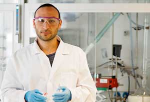
Physicist Dikran Boyaciyan synthesizes polymer brushes in the lab. (Image: Sebastian Keuth)
„This technology is still at an early stage of development. The primary objective is how the interaction between polymer systems and nanoparticles may be tuned and calibrated in a controlled environment,” Boyaciyan explains. Smart polymer materials could be used in chemical nanosensors which report on toxins or cancer cells, monitor parameters of organs or target the release of drugs inside the human body.
Boyaciyan tested two types of pH-insensitive polymers with respect to their prospect for long-term use as sensors: the non-ionic PNIPAM and the cationic PMETAC. The former was found unsuitable because of gold particles being washed out from the brush at high pH values. In the cationic PMETAC brush, however, the gold particles adhered unaffected by pH changes.
Furthermore, Boyaciyan was able to show how to make a reversible pH-switchable composite from PMETAC by incorporating gold nanoparticles and how its complex formation works. In an acidic environment, the particles lose their charge and both particle-particle interactions and particle-brush interactions occur. This leads to a swollen brush because of its chains being less confined.
In contrast, an alkaline environment causes negative charges on the particles and interactions with the positively charged brush are preferred. The chains collapse resulting in a thinner brush layer.
Because of the thickness change also influencing the spectral composition of the reflected light, the material could be used as colorimetric nanosensors. Due to the extremely small dimensions and possible coupling with a miniaturized laser and spectrometer the composite could, in future, be applied in lab-on-a-chip systems or even within the human cell.
Source: TU Darmstadt

Elon Musk spune că nanotehnologia este „BS” – iată cum schimbă deja lumea(Elon Musk says nanotechnology is ‘BS’ – here’s how it’s already changing the world)

Nu poți să spui nanotech fără să creezi grafen. A fost numit un material de minune datorită rezistenței sale, conductivității și elasticității. Făcată din matrice bidimensionale de atomi de carbon aranjate într-un model de tip fagure, foile de grafen se pot întinde doar cu câteva atomi, dar cu o suprafață totală mai aproape de dimensiunea unui poster.
Când este amestecat cu rășini și materiale plastice, materialul rezultat va fi incredibil de puternic și ușor. Materialele compozite pe bază de grafen sunt deja utilizate pentru o gamă largă de aplicații, inclusiv echipamente sportive și panouri de caroserie. Între timp, proprietățile electrice ale grafenului înseamnă că pot îmbunătăți și tehnologiile bateriei.

Posted: Jun 01, 2018

Elon Musk says nanotechnology is ‘BS’ – here’s how it’s already changing the world

(Nanowerk News) You might expect Elon Musk, the business magnate, engineer and serial entrepreneur would be a fan of all things techy. After all, his radical enterprises are built on pushing science to its limit. He’s behind a raft of visionary projects ranging from Tesla’s driverless electric cars and SpaceX’s self-landing reusable rockets to plans for 1,000kph “hyperloop” trains. But it appears there is a size limit to Musk’s technophilia. He recently tweeted that he thinks nanotechnology is “BS”.

So is nanotech just a buzzword used to jazz up some otherwise dull research? Or is it a real branch of scientific discovery that’s actually making a difference to the world?
Nano means small, really small. One nanometre is just one billionth of metre. At this scale we’re dealing with individual molecules and atoms (a carbon atom is about 0.3 nanometres across). So nanotech is about arranging matter that’s between one nanometre and 100 nanometres across in at least one dimension, to create usable medicines, electronics and materials.
The idea of deliberately doing science and engineering at this scale may well have started back in 1959, with a talk entitled There’s Plenty of Room at the Bottom by the great physicist Richard Feynman. But, in fact, people in ancient times used nanotechnology to create stunning works of art, without realising the scales at which they were manipulating matter.

Quantum dots

Today we’ve purposefully harnessed nanotechnology to do some incredible things. Take quantum dots. They may sound like the name of a Belgian indie band but, in fact, these real and incredibly versatile nanomaterials are being used in medical imaging, display technologies and photovoltaic solar cells.
A quantum dot is a particle of semiconducting material just a few nanometres in diameter. Due to their miniscule size, they have electronic properties that sit between what you would expect for a single molecule and a larger bulk material. One of the most useful outcomes of this is that the dots fluoresce (glow) with a colour that depends on the size of the particle. This means that by tweaking the size of the dot you can tune the colours they give off. And that property makes them an ideal candidate for use in your next flat screen TV.

Nanobiotechnology

Nature has a jump on us when it comes to nanotech. The protein molecules that replicate your DNA, digest your food and fight off infections are all nano-sized machines perfectly evolved to do a specific job in your bodies. This makes them ideal places to look for inspiration when trying to engineer something on the nanoscale.
A great example of this in action is a technique known as nanopore DNA sequencing. This technology involves proteins called porins that are normally used by bacteria to allow materials to enter and leave the cells. The porins are placed in a membrane to create channels or pores through it, and an electrical field is then applied. When DNA is forced through the pores the electrical current changes in response to the part of the DNA molecule (the base) that is in the pore.
By measuring the current as the molecule passes through the pore you can work out what the bases that comprise it are and sequence the DNA. This can be done at breakneck speed – up to 450 bases a second – using a tiny desktop device.

Graphene

You can’t mention nanotech without graphene cropping up. It’s been dubbed a wonder material due to its strength, conductivity and elasticity. Made up of two-dimensional arrays of carbon atoms arranged in a honeycomb pattern, graphene sheets can be just a few atoms thick but with a total area nearer the size of a poster.
When mixed with resins and plastics, the resulting material will be incredibly strong and lightweight. Graphene-based composite materials are already being used for a range of applications including sporting equipment and vehicle body panels. Meanwhile graphene’s electrical properties mean it can also enhance battery technologies.
Doesn’t that sound like something an electric car manufacturer might want to look into?
Source: By Mark Lorch, Professor of Science Communication and Chemistry, University of Hull

Lemn pentru supercapacitorii(Wood to supercapacitors)

Oamenii de știință chinezi au găsit acum o modalitate de a face acești electrozi durabil. Aerogelii pot fi obținuți direct din nanofibrili de celuloză, materialul abundent de pereți celulari din lemn.Aerogelii de carbon sunt materiale conductive ultra-laterale cu o suprafață foarte mare. Acestea pot fi preparate prin două căi de producție: primul și cel mai ieftin pornește de la componentele fenolice în cea mai mare parte și produce aerogeluri cu conductivitate improbabilă, în timp ce a doua cale se bazează pe precursori de grafen și nanotuburi de carbon.

Posted: May 24, 2018

Wood to supercapacitors

(Nanowerk News) Carbon aerogels are ultralight, conductive materials, which are extensively investigated for applications in supercapacitor electrodes in electrical cars and cell phones. Chinese scientists have now found a way to make these electrodes sustainably. The aerogels can be obtained directly from cellulose nanofibrils, the abundant cell-wall material in wood, finds the study reported in the journal Angewandte Chemie („Wood-Derived Ultrathin Carbon Nanofiber Aerogels”).

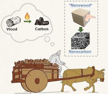
Sustainable highly conductive electrode materials from ultrathin carbon nanofiber aerogels derived from nanofibrillated cellulose
Wood to Supercapacitors. Sustainable highly conductive electrode materials from ultrathin carbon nanofiber aerogels derived from nanofibrillated cellulose. (© Wiley-VCH)
Supercapacitors are capacitors that can take up and release a very large amount of energy in a very short time. Key requirements for supercapacitor electrodes are a large surface area and conductivity, combined with a simple production method. Another growing issue in supercapacitor production—mainly for smartphone and electric car technologies—is sustainability. However, sustainable and economical production of carbon aerogels as supercapacitor electrode materials is possible, propose Shu-Hong Yu and colleagues from the University of Science and Technology of China, Hefei, China.
Carbon aerogels are ultralight conductive materials with a very large surface area. They can be prepared by two production routes: the first and cheapest starts from mostly phenolic components and produces aerogels with improvable conductivity, while the second route is based on graphene- and carbon-nanotube precursors. The latter method delivers high-performance aerogels but is expensive and non-environmentally friendly. In their search for different precursors, Yu and colleagues have found an abundant, far less expensive, and sustainable source: wood pulp.
Well, not really wood pulp, but its major ingredient, nanocellulose. Plant cell walls are stabilized by fibrous nanocellulose, and this extractable material has very recently stimulated substantial research and technological development. It forms a highly porous, but very stable transparent network, and, with the help of a recent technique—oxidation with a radical scavenger called TEMPO—it forms a microporous hydrogel of highly oriented cellulose nanofibrils with a uniform width and length. As organic aerogels are produced from hydrogels by drying and pyrolysis, the authors attempted pyrolysis of supercritically or freeze-dried nanofibrillated cellulose hydrogel.
As it turns out, the method was not as straightforward as expected because ice crystal formation and insufficient dehydration hampered carbonization, according to the authors. Here, a trick helped. The scientists pyrolyzed the dried gel in the presence of the organic acid catalyst para-toluenesulfonic acid. The catalyst lowered the decomposition temperature and yielded a “mechanically stable and porous three-dimensional nanofibrous network” featuring a “large specific surface area and high electrical conductivity,” the authors reported.
The authors also demonstrated that their wood-derived carbon aerogel worked well as a binder-free electrode for supercapacitor applications. The material displayed electrochemical properties comparable to commercial electrodes. The method is an interesting and innovative way in which to fabricate sustainable materials suitable for use in high-performance electronic devices.
Source: Wiley

Nano blocul de construcție are un arc(New nano building block takes a bow)

Nanotuburile de nitrura de bor sunt pregatite pentru a deveni blocuri eficiente pentru materialele compozite de ultima generatie si materialele polimerice bazate pe o descoperire noua la Universitatea Rice.Nanotuburile de nitrura de bor, ca și verii lor de carbon, sunt foi laminate din matrice hexagonale. Spre deosebire de nanotuburile de carbon, ele sunt hibrizi izolatori electrici, alcătuit din atomi de bor și atomi de azot alternativi.
Izolarea nanotuburilor care pot fi funcționalizate va fi un element important de construcție pentru proiectele de nanoengineering.

Posted: May 21, 2018

New nano building block takes a bow

(Nanowerk News) Boron nitride nanotubes are primed to become effective building blocks for next-generation composite and polymer materials based on a new discovery at Rice University – and a previous one.

Scientists at known-for-nano Rice have found a way to enhance a unique class of nanotubes using a chemical process pioneered at the university. The Rice lab of chemist Angel Martí took advantage of the Billups-Birch reaction process to enhance boron nitride nanotubes.
The work is described in the American Chemical Society journal ACS Applied Nano Materials(„Chemical Decoration of Boron Nitride Nanotubes Using the Billups-Birch Reaction: Toward Enhanced Thermostable Reinforced Polymer and Ceramic Nanocomposites”).
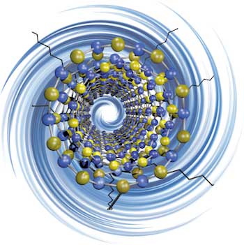
decorating electrically insulating boron nitride nanotubes with functional groups
Rice researchers have discovered a way to “decorate” electrically insulating boron nitride nanotubes with functional groups, making them more suitable for use with polymers and composite materials. (Image: Martí Research Group)
Boron nitride nanotubes, like their carbon cousins, are rolled sheets of hexagonal arrays. Unlike carbon nanotubes, they’re electrically insulating hybrids made of alternating boron and nitrogen atoms.
Insulating nanotubes that can be functionalized will be a valuable building block for nanoengineering projects, Martí said. “Carbon nanotubes have outstanding properties, but you can only get them in semiconducting or metallic conducting types,” he said. “Boron nitride nanotubes are complementary materials that can fill that gap.”
Until now, these nanotubes have steadfastly resisted functionalization, the “decorating” of structures with chemical additives that allows them to be customized for applications. The very properties that give boron nitride nanotubes strength and stability, especially at high temperatures, also make them hard to modify for their use in the production of advanced materials.
But the Billups-Birch reaction developed by Rice Professor Emeritus of Chemistry Edward Billups, which frees electrons to bind with other atoms, allowed Martí and lead author Carlos de los Reyes to give the electrically inert boron nitride nanotubes a negative charge.
That, in turn, opened them up to functionalization with other small molecules, including aliphatic carbon chains.
“Functionalizing the nanotubes modifies or tunes their properties,” Martí said. “When they’re pristine they are dispersible in water, but once we attach these alkyl chains, they are extremely hydrophobic (water-avoiding). Then, if you put them in very hydrophobic solvents like those with long-chain hydrocarbons, they are more dispersible than their pristine form.
Transmission electron microscope images show a pristine boron nitride nanotube at left and functionalized nanotube at right
Transmission electron microscope images show a pristine boron nitride nanotube at left and functionalized nanotube at right. Rice University scientists have developed a method to make insulating boron nitride nanotubes better able to use in composite materials. (Image: Martí Research Group)
“This allows us to tune the properties of the nanotubes and will make it easier to take the next step toward composites,” he said. “For that, the materials need to be compatible.”
After he discovered the phenomenon, de los Reyes spent months trying to reproduce it reliably. “There was a period where I had to do a reaction every day to achieve reproducibility,” he said. But that turned out to be an advantage, as the process only required about a day from start to finish. “That’s the advantage over other processes to functionalize carbon nanotubes. There are some that are very effective, but they may take a few days.”
The process begins with adding pure ammonia gas to the nanotubes and cooling it to -70 degrees Celsius (-94 degrees Fahrenheit). “When it combines with sodium, lithium or potassium — we use lithium — it creates a sea of electrons,” Martí said. “When the lithium dissolves in the ammonia, it expels the electrons.”
The freed electrons quickly bind with the nanotubes and provide hooks for other molecules. De los Reyes enhanced Billups-Birch when he found that adding the alkyl chains slowly, rather than all at once, improved their ability to bind.
The researchers also discovered the process is reversible. Unlike carbon nanotubes that burn away, boron nitride nanotubes can stand the heat. Placing functionalized boron nitride tubes into a furnace at 600 degrees Celsius (1,112 degrees Fahrenheit) stripped them of the added molecules and returned them to their nearly pristine state.
“We call it defunctionalization,” Martí said. “You can functionalize them for an application and then remove the chemical groups to regain the pristine material. That’s something else the material brings that is a little different.”
Source: By Mike Williams, Rice University

Noua tehnică relevă o formă 3D a interacțiunii polaritonului nanostructurii(New technique reveals 3D shape of nanostructure’s polariton interaction)

Din cauza conductivității, flexibilității, transparenței și rezistenței, grafenul are potențialul de a crea celule solare mai eficiente, circuite electrice și microcipuri mai mici și mai rapide, ecrane transparente, condensatori de înaltă densitate și baterii.Apoi am adunat informații la diferite distanțe tip eșantion și am combinat toate aceste informații stratificate împreună pentru a obține imaginea tomografică și a dezvălui structura polaritonului 3-D”.

Posted: May 21, 2018

New technique reveals 3D shape of nanostructure’s polariton interaction

(Nanowerk News) Because of its conductivity, flexibility, transparency and strength, graphene has the potential to create more efficient solar cells, smaller and faster electric circuits and microchips, transparent displays, and high density capacitors and batteries.

According to Xiaoji Xu, assistant professor in the Department of Chemistry at Lehigh University, another quality that makes nanomaterials like graphene so special is their ability to generate a physics phenomenon called a polariton.
Polaritons are quasiparticles resulting from a strong coupling of electromagnetic waves with an electric or magnetic dipole-carrying excitation–referred to by some as a light-matter coupling. Polaritons make it possible for nanostructures to confine–and compress–light around the material.
The ability to compress light is key to scaling down devices for future optical communications and computing. It could also lead to sensing at a scale below one nanometer, important for achieving biomedical advances in disease detection, prevention and treatment.
The challenge for people studying these materials, says Xu, is how to reveal–and characterize–the polaritons at the nanoscale because no conventional microscope can do that.
Now Xu and his team have found a way to reveal the 3-D shape of the polariton interaction around a nanostructure. Their technique improves upon the common spectroscopic imaging technique known as scattering-type scanning near-field optical microscopy (s-SNOM). The team’s method, called peak force scattering-type scanning near-field optical microscopy (PF-SNOM), works through a combination of peak force tapping mode and time-gated light detection.
The researchers have detailed their work in an article in Nature Communications („Tomographic and multimodal scattering-type scanning near-field optical microscopy with peak force tapping mode”).
In the paper, the authors state: „PF-SNOM enables direct sectioning of vertical near-field signals from a sample surface for both three-dimensional near-field imaging and spectroscopic analysis. Tip-induced relaxation of surface phonon polaritons are revealed and modeled by considering tip damping.”
According to the researchers, PF-SNOM also offers an improved spatial resolution of five nanometers, rather than the typical ten nanometers offered by the traditional s-SNOM.
„Our technique could be beneficial to scientists studying nanostructures enabling them to better understand how the electrical field is distributed around a given nanostructure,” says Xu.
Their PF-SNOM characterization method is not only more direct than existing techniques, it can also simultaneously obtain the polaritonic, mechanical and electrical information.
With one measurement, explains Xu, multiple modes of information can be obtained–a unique advantage.
The development of PF-SNOM grew out of the team’s study of gap mode, when two plasmonic structures approach within a few nanometers there is a huge enhancement of the plasmon intensity in the gap between the two structures as energy is transferred from one structure to the other. With their ability to narrow this gap mode response in simulations, the researchers decided to try to extend it to non-gap mode – when increasing the distance between the atomic force microscopy (AFM) probe tip and the sample.
„Using an AFM tip, we measured the scattered light as a function of tip-sample distance,” explains Wang, a PhD student in Xu’s lab and a co-author on the paper. „We then gathered information at different tip-sample distances and combined all this layered information together to obtain the tomographic image and reveal the 3-D polariton structure.”
Interestingly, when the team began their experiments they expected a different outcome. However, during the simulations, they observed a special shape of light scattering and saw there was an obvious gap mode enhancement.
„It turned out that we could section the light in different tip-samples distances and use those signals to view the near-field response at different layers and in vertical directions,” says Wang.
He adds: „Though this work was done with infrared, in principle it could also be extended to other frequencies, such as visible and terahertz.”
Source: Lehigh University

Grafenul deschide calea către comunicațiile optice rapide de mare viteză(Graphene paves the way to faster high-speed optical communications)

utorii au descoperit din nou ceva unic in ceea ce priveste grafenul: tuneabilitatea THG pe o lungime larga a lungimii de unda.Deoarece tot mai multe aplicatii sunt all-optice, aceasta lucrare deschide calea catre o multitudine de tehnologii

Posted: May 21, 2018

Graphene paves the way to faster high-speed optical communications

(Nanowerk News) Graphene, among other materials, can capture photons, combine them, and produce a more powerful optical beam. This is due to a physical phenomenon called the optical harmonic generation, which is characteristic of nonlinear materials. Nonlinear optical effects can be exploited in a variety of applications, including laser technology, material processing and telecommunications.

Although all materials should present this behaviour, the efficiency of this process is typically small and cannot be controlled externally. Now, partners of the Graphene Flagship project in Cambridge (UK), Milan, and Genova (Italy) have demonstrated for the first time that graphene not only shows a good optical response, but also how to control the strength of this effect using an electric field (Nature Nanotechnology, „Broadband, electrically tuneable, third harmonic generation in graphene”).
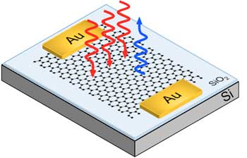
Third Harmonic Generation in Graphene
Electrical control of third harmonic generation (THG) can be obtained in single-layer graphene. In THG three low-frequency photons (red) sum up to generate one high-frequency (blue) photon. For this reason, THG can be used for optical frequency converters. (Image: Giancarlo Soavi, University of Cambridge)
Researches envision the creation of new graphene optical switches, which could also harness new optical frequencies to transmit data along optical cables, increasing the amount of data that can be transmitted. Currently, most commercial devices using nonlinear optics are only used in spectroscopy. Graphene could pave the way towards the fabrication of new devices for ultra-broad bandwidth applications.
„Our work shows that the third harmonic generation efficiency in graphene can be increased by over 10 times by tuning an applied electric field,” explains Giancarlo Soavi, lead author of the paper and researcher at the Cambridge Graphene Centre (University of Cambridge, UK).
„The authors found again something unique about graphene: tuneability of THG over a broad wavelength range. As more and more applications are all-optical, this work paves the way to a multitude of technologies,” said said ICREA Professor Frank Koppens from ICFO (The Institute of Photonic Sciences), Barcelona, Spain, who is the leader of the Photonics and Optoelectronics Work Package within the Graphene Flagship.
Professor Andrea C. Ferrari, Science and Technology Officer of the Graphene Flagship, and Chair of its Management Panel, added how „graphene never ceases to surprise us when it comes to optics and photonics.” He also highlights that „the Graphene Flagship has put significant investment to study and exploit the optical properties of graphene. This collaborative work could lead to optical devices working on a range of frequencies broader than ever before, thus enabling a larger volume of information to be processed or transmitted.”
Source: By Sian Fogden, Graphene Flagship

O soluție ușoară la problema dificilă de stocare a energiei(A soft solution to the hard problem of energy storage)

Realizăm o nouă lume a acestor materiale 2-D care pot fi utilizate pentru aplicații industriale reale, care se potrivesc cu standardul din industrie și încearcă să facă din acesta un dispozitiv real. După mai mult de un deceniu de muncă în materiale 2-D, am găsit o cale de trecere peste una dintre cele mai mari bariere în calea aplicării și de fapt creăm un sistem care este una dintre cele mai plauzibile modalități de a împinge aceste materiale în industrie „.Cercetătorii au lucrat la utilizarea materialelor bidimensionale, a nanomaterialelor subțiri atomice, ca componente pentru încărcarea mai rapidă, baterii cu durată mai lungă de funcționare și supercapacitoare

Posted: May 18, 2018

A soft solution to the hard problem of energy storage

(Nanowerk News) It’s great in the lab, but will it actually work? That’s the million-dollar question perpetually leveled at engineering researchers. For a family of layered nanomaterials, developed and studied at Drexel University — and heralded as the future of energy storage — that answer is now, yes.

For some time, researchers have been working on using two-dimensional materials, atomically thin nanomaterials, as components for faster-charging, longer-lasting batteries and supercapacitors. But the problem with the existing techniques for doing so are that when the thickness of the material layer is increased to about 100 microns — roughly the width of a human hair, which is the industry standard for energy storage devices — the materials lose their functionality.
Recently published research from Drexel and the University of Pennsylvania, shows a new technique for manipulating two-dimensional materials that allows them to be shaped into films of a practically usable thickness, while maintaining the properties that make them exceptional candidates for use in supercapacitor electrodes.
The study, published in the journal Nature („Thickness-independent capacitance of vertically aligned liquid-crystalline MXenes”), focuses on using soft materials — similar to those in the liquid crystal displays of phones and televisions — as a guide for self-assembly of MXene sheets. MXenes, are a class of nanomaterials discovered at Drexel in 2011, that are particularly well-suited for energy storage.
“Our method relies on a marriage between soft material assembly and functional 2-D nanomaterials,” said Yury Gogotsi, PhD, Distinguished University and Bach professor in Drexel’s College of Engineering, who was a co-author of the research. “The resulting electrode films show rapid ion transport, outstanding rate handling, and charge storage equal to or exceeding commercial carbon electrodes.”
Soft assembly of MXene allows the 2-D materials to be stacked vertically, maintaining ion diffusion as the thickness of the material is increased
Soft assembly of MXene allows the 2-D materials to be stacked vertically, maintaining ion diffusion as the thickness of the material is increased. (click on image to enlarge)

An Open Channel

According to co-author Yu Xia, PhD, a postdoctoral fellow in Penn’s School of Engineering and Applied Science, the challenge of maintaining the energy density (how much energy the devices can store) and power density (how fast the device can charge) of a charge storing material lies in maintaining clear channels for ion movement as the materials are scaled up to larger sizes.
“The ion diffusion problem in energy storage devices,” Xia says, “including batteries and supercapacitors, has been long recognized as one of the major issues impeding the industrial development of new batteries and supercapacitors with higher energy and power density. Conventionally, 2-D materials intend to stack on top of each other like sheets of paper in a book, resulting in a prolonged ion diffusion length, which suppresses their performance when the thickness of the electrode approaches industrial standards.”
The team’s method avoids this stacking problem, which inhibits ion diffusion, by propping the MXene flakes in the electrodes vertically. At the microscopic level, it might look something like standing up toothpicks in silly putty. In addition to getting them to align vertically, their orientation can also be adjusted by moving the soft material base.
The team’s melding of soft matter assembly with hard materials yielded promising results for MXene’s future as an energy storage material.
“MXene electrodes prepared by this method show normalized capacitance which is almost independent of thickness up to at least 200 microns, which is not the case for conventionally assembled electrodes, where the MXene flakes would be aligned parallel to the electrode surface,” according to Tyler Mathis, a doctoral student in Drexel’s Department of Materials Science and Engineering and co-author of the research, who performed all electrochemical testing of the materials.

Stand and Deliver

While “soft matter self-assembly” — the process by which molecules inside a material align themselves in an orientation that researchers can manipulate — has been around since the 1970s, and is now the driving force behind television, phone and laptop displays, combining it with hard materials is a significant breakthrough.
Although a couple of research groups have been able to engineer vertical alignment of materials using a top-down process, these routes are difficult to scale up for industrial applications.
“Our process is through self-assembly,” said Shu Yang, PhD, a professor in the departments of Materials Science and Engineering, and Chemical and Biomolecular Engineering in Penn’s School of Engineering and Applied Science and a co-author of the research. “So it’s much cheaper and can be scalable over a large area. In the end, it’s the concept of using soft materials with interesting alignment and ordering through assembly to align hard materials with interesting nanostructures and functionality that is the biggest breakthrough.”
To get the 2-D material to undergo this process, the researchers used a surfactant, which can squeeze between the MXene layers to help them form a liquid crystal phase. The researchers then applied a mechanical shearing method to it, which forced the molecules to align the MXene films vertically. The vertical channels allow ions to move, or diffuse — which is the key to MXene’s properties — even as the material is scaled up in thickness.
“There’s a lot of fundamental knowledge in liquid crystals,” Yang said. “People think it’s an old technology, but we just keep rediscovering that this knowledge is actually very useful and applicable to new functional materials.”

Next in Line

Although the researchers acknowledge that there are other challenges to overcome before the method can be used in real world devices, they believe their findings provide an exciting leap forward in the field. The long-term goals are to apply the method to supercapacitor and battery electrodes for powering mobile electronic devices, electric cars, and use in renewable energy harvesting technologies.
“It’s a perfect marriage between soft matter self-assembly and nanomaterials,” Xia says. “We’re making a new world of these 2-D materials that can be used towards real industry applications, matching up with the industry standard and trying to make a real device out of it. After more than a decade of work in 2-D materials, we have found a way past one of the biggest barriers to application and are actually creating a system that is one of the most plausible ways to push these materials into industry.”
Source: Drexel University

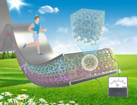
Flexibilitate, foarte eficientă recoltare de energie multimodală(Flexible, highly efficient multimodal energy harvesting)

„Vedem că acest compozit 3D are o putere de producție mult mai mare în diferite moduri”, a spus Wang. Putem să o întindem, să o îndoim, să o apăsăm. Și, în același timp, poate fi folosit ca recoltă de energie pirolectrică dacă există un gradient de temperatură de cel puțin câteva grade. „Dar aceste materiale sunt relativ ineficiente, deoarece, la încărcarea mecanică, energia mecanică este în cea mai mare parte absorbită de cea mai mare parte a polimerului, cu o fracțiune foarte mică transferată la nanoparticulele piezo. În timp ce adăugați mai mult ceramică ar crește eficiența energetică, vine cu compromisul de flexibilitate mai mică.

Posted: May 17, 2018

Flexible, highly efficient multimodal energy harvesting

(Nanowerk News) A piezoelectric ceramic foam supported by a flexible polymer support provides a 10-fold increase in the ability to harvest mechanical and thermal energy over standard piezo composites, according to Penn State researchers (Energy and Environmental Science, „Flexible three-dimensional interconnected piezoelectric ceramic foam based composites for highly efficient concurrent mechanical and thermal energy harvesting”).

A flexible ceramic foam for energy harvesting
A flexible ceramic foam for energy harvesting. (Image: Wang Lab/Penn State)
In the search for ways to harvest small amounts of energy to run mobile electronic devices or sensors for health monitoring, researchers typically add hard ceramic nanoparticles or nanowires to a soft, flexible polymer support. The polymer provides the flexibility, while the piezo nanoparticles convert the mechanical energy into electrical voltage.
But these materials are relatively inefficient, because upon mechanical loading the mechanical energy is largely absorbed by the bulk of the polymer, with a very small fraction being transferred to the piezo nanoparticles. While adding more ceramic would increase the energy efficiency, it comes with the tradeoff of less flexibility.
“The hard ceramics in the soft polymer is like stones in water. You can slap the surface of the water, but little force is transferred to the stones,” said Qing Wang, professor of materials science and engineering, Penn State. “We call that strain-transfer capability.”
Almost three decades ago, the late Penn State materials scientist Bob Newnham came up with the concept that the connectivity of the piezo filler determined the efficiency of the piezoelectric effect. A three-dimensional material would be more efficient than what he classified as 0D nanoparticles, 1D nanowires or 2D films, because the mechanical energy would be transported directly through the 3D material instead of dissipating into the polymer matrix.
“Bob Newnham was a legend in the field of piezoelectrics,” said Wang, “So everybody in the ceramic community knew of his approach, but how to achieve that 3D structure with a well-defined microstructure remained a mystery.”
The secret ingredient to solve the mystery turned out to be a cheap polyurethane foam dusting sheet that can be purchased at any home improvement store. The small uniform protrusions on the sheet act as a template for forming the microstructure of the piezoelectric ceramic. The researchers applied the ceramic to the polyurethane sheet in the form of suspended nanoparticles in solution. When the template and solution are heated to a high enough temperature, the sheet burns out and the solution crystalizes into a solid 3D microform foam with uniform holes. They then fill the holes in the ceramic foam with polymer.
“We see that this 3D composite has a much higher energy output under different modes,” said Wang. “We can stretch it, bend it, press it. And at the same time, it can be used as a pyroelectric energy harvester if there is a temperature gradient of at least a few degrees.”
The other corresponding author on the new paper in the high-impact journal Energy and Environmental Science is Sulin Zhang, professor of engineering science and mechanics, Penn State. Zhang and his students were responsible for extensive computational work simulating the piezoelectric performance of the 3D composite.
Said Zhang, “We were able to show theoretically that the piezoelectric performance of nanoparticle/nanowire composites is critically limited by the large disparity in stiffness of the polymer matrix and piezoceramics, but the 3D composite foam is not limited by stiffness. This is the fundamental difference between these composite materials, which speaks to the innovation of this new 3D composite. Our extensive simulations further demonstrate this idea.”
Currently, Wang and collaborators are working with lead-free and more environmentally friendly alternatives to the current lead-zirconium-titanate (PZT) ceramic.
“This is a very general method,” said Wang. “This is to demonstrate the concept, based on Bob Newnham’s work. It is good to continue the work of a Penn State legend and to advance this field.”
Source: Penn State Materials Research Institute