Ipoteza puternică a lui Ivy ar putea conduce la adezivi medicali mai buni, la armura de luptă mai puternică(Ivy’s powerful grasp could lead to better medical adhesives , stronger battle armor)

Zhang a spus particule bogate in aceste proteine ​​au abilitati exceptionale de adeziv -abilitati care ar putea fi folosite in avantajul multor, de la ingineri biomedicale la producatorii de vopsea

Ivy's

Superacidul este un medicament bun pentru semiconductorii subțiri(Superacids are good medicine for super thin semiconductors)

Tratarea semiconductorului 2-D cu un superacid vindecă defectele structurale și îmbunătățește performanța electronică a materialului. au implementat un tratament superacid pentru defectele de vindecare în filmele subțiri MoS 2 . Aceștia au arătat că acest tratament chimic simplu este compatibil cu fabricarea dispozitivelor electronice ( Applied Physics Letters , „Proprietățile materialelor și ale dispozitivelor disulfurului de molibden monolayer tratat cu superacid” )

Posted: Apr 10, 2018

Superacids are good medicine for super thin semiconductors

(Nanowerk News) Designing wearable sensors or other devices demands robust, flexible electronics. Extremely thin films, just one atom thick, such as molybdenum disulfide (MoS2), hold promise. Large-area synthesis of these materials is required for their commercialization. But today’s thin films are plagued by structural defects. These defects degrade device performance.

Scientists at New York University and the Center for Functional Nanomaterials have implemented a superacid treatment for healing defects in thin MoS2 films. They showed that this straightforward chemical treatment is compatible with electronic device fabrication (Applied Physics Letters, „Material and device properties of superacid-treated monolayer molybdenum disulfide”). Also, the process boosts device performance by reducing the density of defects in the material.
2-D molybdenum disulfide semiconductor
(Top) Illustration shows a 2-D molybdenum disulfide (MoS2) semiconductor with structural defects such as missing surface atoms. (Bottom) Treating the 2-D semiconductor with a superacid heals structural defects and improves the electronic performance of the material. (Image: Brookhaven National Laboratory)
Wearable computers are an emerging trend. To capitalize on this trend, industry needs mechanically flexible devices. Thin films can enable power-efficient and high-speed devices. This work is a vital step toward realizing wearable devices.
The atomically thin nature of layered 2-D semiconductors gives rise to a gamut of unique physical properties, which often do not exist in traditional bulk semiconductors such as silicon. These physical properties can enable a new family of devices, from sensors to logic switches, that have superior performance compared with their conventional counterparts.
Producing defect-free 2-D materials on a large scale underpins the translation of basic scientific studies into real products. However, synthetic 2-D materials are plagued with large numbers of defects that suppress many of their useful properties.
In the ongoing quest to achieve large defect-free 2-D semiconductors, scientists at New York University have shown that a superacid treatment boosts the performance of devices made from monolayer 2-D MoS2. In collaboration with scientists at the Center for Functional Nanomaterials, they used an advanced material characterization technique, called Nano-Auger, to study the structure of 2-D MoS2 on the atomic scale. They discovered that the superacid treatment is mostly effective in healing defects in the regions of MoS2 that have missing sulfur atoms.
These findings are important steps toward realizing high-performance devices from synthetic 2-D semiconductors.
Source: U.S. Department of Energy, Office of Science

Aliajul nanostructurat cu oxigen(Nanostructured alloying with oxygen)

pentru a produce materiale nanostructurate cu compoziții personalizate și fără efortul de precasting. Acestea permit producerea de noi materiale nanocristaline metalice prin aliaje mecanice ale elementelor nemiscibile. Contaminarea cu oxizi în timpul procesării acestor pulberi încă împiedică această metodă să fie aplicată în industrie în mod cuprinzător.

Posted: Apr 09, 2018

Nanostructured alloying with oxygen

(Nanowerk News) Severe plastic deformation and powder processing techniques are used to produce nanostructured materials with tailor-made compositions and without the effort of precasting. They allow the production of novel metallic nanocrystalline materials by mechanically alloying immiscible elements. Oxide contamination during the processing of these powders still hinders this method to be applied in industry comprehensively.

Meanwhile it is also known that oxygen could be used beneficially to influence morphology, mechanical properties and thermal stability of nanostructured alloys. Up to now this possibility is still not used as it is unclear how oxide behaves during annealing.
Scientists from the Max-Planck-Institut für Eisenforschung (MPIE), the Austrian Erich Schmid Institute of Material Science, the Universities Leoben and Graz (Austria) and the Chinese Hubei University analysed in-situ copper-iron alloys during annealing to find out when and how oxide is formed and how it can be used to strengthen nanocrystalline materials. They published their latest findings in Nature Communications („In situ atomic-scale observation of oxidation and decomposition processes in nanocrystalline alloys”).
Dr. Jazmin Duarte
Dr. Jazmin Duarte did atom probe tomography measurements to characterize the sample and see the oxide distribution. (Image: Max-Planck-Institut für Eisenforschung)
“By combining different experimental methods and density-functional theory calculations, we studied the thermal behaviour of oxygen in nanocrystalline copper-iron alloys which were fabricated under severe deformation and high pressure. During the heating process but still at very low temperatures, oxidation starts, leading to the formation of nanosized copper and iron oxides inside grains. Later in the heating process the metastable copper-iron solid solution decomposes into iron- and copper-rich phases,” explains Dr. Jazmin Duarte, senior researcher in the department “Structure and Nano-/Micromechanics of Materials”.
The copper and iron oxides and iron precipitates grow with annealing temperature, till they reach approximately 10 nanometres. Both oxide distributions are almost identical, which means that oxygen diffuses to one specific area during heating, simultaneously triggering the nucleation processes of oxides.
“For the first time a direct observation of oxide formation in single-phase copper-iron alloys was possible. We also did several comparison studies and ex situ analyses to make sure that neither the electron beam of the transmission electron microscope nor the sample size have an influence on the oxidation and precipitation processes. This new insights give us the possibility of manipulating mechanical properties by including oxygen into nanocrystalline alloys. Oxygen which was formerly seen as contamination to be avoided, can now be used as an ingredient to form advanced, nanostructured alloys,” explains Prof. Gerhard Dehm, director at the MPIE.
The scientists are now further studying the mechanisms by which oxygen can be introduced into the alloys and how the microstructure and consequently the mechanical behaviour are affected by an increased content of dissolved oxygen. Such tailor-made microstructures could be then used to engineer oxide strengthened nanocrystalline materials for specific applications.
Source: Max-Planck-Institut für Eisenforschung

Celuloza fotonica iridescenta, imitand culoarea structurala a insectelor, cu aplicatii optice(Iridescent photonic cellulose, mimicking the structural color of insects, with optical applications)

creează pentru prima dată cristale fotonice și structuri plasmonice a unui derivat de celuloză prin nanostructurarea sa cu tehnica de litografie moale. Prin nanostructarea periodică a filmului de celuloză, acesta nu mai este transparent și începe să reflecte culori intense, în funcție de modelul cu care a fost turnat.

Posted: Apr 09, 2018

Iridescent photonic cellulose, mimicking the structural color of insects, with optical applications

(Nanowerk News) The bright colors of some butterflies, beetles or birds are not due to the presence of pigments that selectively absorb light, but due to the so-called structural coloration. Structural coloration occurs on surfaces with a nanostructure with dimensions similar to those of the wavelength of the incident light (typically below the micron). These ordered nanostructures are known as photonic crystals. There is a great interest in providing cellulose, the most abundant polymer in earth, biocompatible and biogradable, with these structures, which can offer new optical and electric functionalities.

The study published today in Nature Photonics („Hydroxypropyl cellulose photonic architectures by soft nanoimprinting lithography”), led by Dr. Agustín Mihi of the Institute of Materials Science of Barcelona (ICMAB-CSIC), creates for the first time photonic crystals and plasmonic structures of a cellulose derivative through its nanostructuring with the soft lithography technique. By periodically nanostructuring the cellulose film, it is no longer transparent and begins to reflect intense colors, depending on the pattern with which it has been molded.
The colors obtained do not depend on pigments but on nanostructures that interact differently with the incident light, therefore presenting different colors
The colors obtained do not depend on pigments but on nanostructures that interact differently with the incident light, therefore presenting different colors. (Image: ICMAB)
With this new, fully scalable and low cost technique, alternative to the traditional self-assembly of cellulose nanocrystals, a high quality and reproducible nanostructure is created on this polymer in a very short time, and achieving a wide range of iridescent colors, only depending on the size and morphology of the created structures.
These photonic crystals can be nanoimprinted on different substrates to provide photonic properties on surfaces that do not present this property, such as paper, demonstrating the potential of this technology as photonic ink, for applications in anti-counterfeiting technology, packaging, decorative paper, labels or sensors, among others.
When these structures are covered with a thin metal layer, they acquire plasmonic properties while maintaining their flexibility, achieving brighter colors. Furthermore, depending on the type of cellulose derivative used, its degree of biodegradability and solubility in water can be tuned. These plasmonic structures can be used as disposable sensors for Raman emission or to increase the light emitted by a dye.
Photonic crystals and plasmonic architectures are used in optics for their ability to manipulate light. In this work, these interesting optical properties are obtained in a biocompatible and biodegradable material, which can open up new fields of application. The study has been funded by the European Research Council (ERC Sarting Grant) through the the ENLIGHTMENT project, and by the Severo Ochoa project of the ICMAB.

Source: ICMAB

Cercetările solide determină fizicienii să propună o nouă stare de materie(Solid research leads physicists to propose new state of matter)

propunerea unui nou tip de materie care este atât superfluid cât și quasicrystal.Un supersolid este un lichid care curge fără frecare ale cărui atomi sunt de asemenea aranjate într-un mod periodic, la fel cum sunt într-un solid de cristal”, a spus el. „Aceste două stări, care se exclud reciproc în viața noastră de zi cu zi, pot exista în același timp în același material fizic în lumea cuantică”.

Posted: Apr 09, 2018

Solid research leads physicists to propose new state of matter

(Nanowerk News) The term „superfluid quasicrystal” sounds like something a comic-book villain might use to carry out his dastardly plans.

In reality, it’s a new form of matter proposed by theoretical physicists at The University of Texas at Dallas in a recent study published in the journal Physical Review Letters („Superfluid-Quasicrystal in a Bose-Einstein Condensate”). Their study also describes a „recipe” for making the exotic materials in the lab.
From left: The research team includes doctoral student Junpeng Hou; Dr. Kuei Sun, senior lecturer; Dr. Chuanwei Zhang, professor of physics; and Dr. Haiping Hu, a postdoctoral research associate
From left: The research team includes doctoral student Junpeng Hou; Dr. Kuei Sun, senior lecturer; Dr. Chuanwei Zhang, professor of physics; and Dr. Haiping Hu, a postdoctoral research associate.
Most people are familiar with the three fundamental states of matter: solid, liquid and gas. There are actually several more, including plasma, which is found inside the sun and other stars, and Bose-Einstein condensates, which are very dense and exist only at the most extreme cold temperatures.
A superfluid is an exotic state of matter with unusual properties. It has zero viscosity, which means it can flow across a surface and not slow down – or lose any energy – due to friction with the surface. Superfluids, such as liquid helium, must be cooled to extremely low temperatures for such properties to emerge.
„If your morning coffee was a superfluid, and you stirred it with a spoon, you could remove the spoon and the coffee would never stop moving,” said Dr. Chuanwei Zhang, professor of physics in the School of Natural Sciences and Mathematics and corresponding author of the study. „Regular fluids will eventually stop due to friction with the cup.”

Both a Superfluid and a Quasicrystal

About 50 years ago, researchers proposed a new type of matter that combined the properties of a superfluid with those of a solid crystal. Dubbed a supersolid, it’s only been in the past couple of years that scientists have been able to produce that unusual material in the lab.
„In physics, we have a very strict definition of what a fluid is and what a solid is,” Zhang said. „Liquid water cannot behave as a solid, and vice versa. They can be mixed together, for example in a glass of ice water, but they are still separate forms of matter.”
In the world of quantum physics, which describes how matter behaves at the level of atoms and individual particles, this is not always true, Zhang said.
„A supersolid is a fluid flowing without friction whose atoms are also arranged in a periodic way, just as they are in a crystal solid,” he said. „These two states, which are mutually exclusive in our everyday life, can exist at the same time in the same physical material in the quantum world.”
In their new study, Zhang and his colleagues suggest the next logical step – proposing a new type of matter that is both a superfluid and a quasicrystal.
A crystal, like table salt, has atoms that are arranged in a highly ordered, periodic pattern that is unchanged when you rotate or repeat it, Zhang said. A checkerboard can be thought of as a two-dimensional crystal. Quasicrystals, on the other hand, are materials whose atoms are ordered and have structure like in a crystal, but their arrangement is not periodic – it does not repeat.
„We asked the question, can you have a new quantum matter state that is both a quasicrystal and a superfluid?” Zhang said.
The answer is yes, at least from physical principles, Zhang said.
The material Zhang and his colleagues propose should flow without friction while also exhibiting a nonperiodic, quasicrystal structure.
„This is a theory at the moment, but in this paper we suggest an experimental setup similar to the experiment that produced the first supersolids,” Zhang said. „The good news is, we shouldn’t have to invent any new technology to actually make this material. It basically involves shooting lasers at a Bose-Einstein condensate.”
Junpeng Hou, the lead author of the study and a physics PhD student at UT Dallas, said producing the material might still be challenging.
„It can take several years for new supersolids to become experimentally realized,” Hou said. „But I believe our system would not take that long, maybe one or two years.”
Source: University of Texas at Dallas

Un nou mod de a substitui materialele atomice(A new way to atomically thin materials)

Materialele bidimensionale, formate din straturi extrem de subți, cu grosime de câteva atomi, au proprietăți unice care sunt complet diferite de versiunile normale tridimensionale. Un exemplu proeminent al acestui lucru este grafenul, care este format din straturi unice de atomi de carbon. În 2011, a fost sintetizată o nouă clasă de materiale bidimensionale la Universitatea Drexel din Philadelphia (Pennsylvania, SUA).
Cunoscute ca MXenes, materialele sunt fabricate din carburi metalice de tranziție și nitruri, unde M reprezintă un metal de tranziție, cum ar fi titan, vanadiu sau molibden, X poate fi carbon și / sau azot și sunt disponibile multe compoziții (circa 30 au fost deja demonstrate experimental și se așteaptă zeci de alte). Un astfel de MXene este carbură de titan, Ti 3 C 2 .

Posted: Apr 09, 2018

A new way to atomically thin materials

(Nanowerk News) Metallic conductivity and hydrophilicity of MXenes have established them as electrodes in rechargeable batteries and supercapacitors, as well as other applications, including photothermal cancer therapy, electromagnetic shielding, water purification and gas sensing.

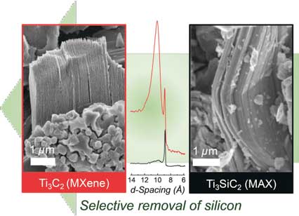
In the journal Angewandte Chemie („Selective Etching of Silicon from Ti3SiC2 (MAX) To Obtain 2D Titanium Carbide (MXene)”), researchers have now introduced a new production method. Instead of using conventional, yet more expensive, titanium aluminum carbide, they selectively etch silicon out of titanium silicon carbide, a cheaper and more common precursor, to synthesize titanium carbide.
Silicon secedes: titanium carbide flakes obtained by selective etching of titanium silicon carbide
A new way to atomically thin materials – Silicon secedes: titanium carbide flakes obtained by selective etching of titanium silicon carbide. (© Wiley-VCH)
Two-dimensional materials, consisting of extremely thin layers that are a few atoms thick, have unique properties that are completely different than the normal three-dimensional versions. A prominent example of this is graphene, which is made of single layers of carbon atoms. In 2011, a new class of two-dimensional materials was synthesized at Drexel University in Philadelphia (Pennsylvania, USA).
Known as MXenes, the materials are made of transition metal carbides and nitrides, where the M stands for a transition metal, such as titanium, vanadium, or molybdenum, X can be carbon and/or nitrogen, and many compositions are available (about 30 have already been experimentally demonstrated and dozens more are expected). One such MXene is titanium carbide, Ti3C2.
Obtaining the desired MXene usually involves a roundabout process: Layered carbides and nitrides, known as MAX phases, are selectively etched with hydrofluoric acid to remove the layers of the “A” element, which is a group 13 or 14 element such as aluminum, silicon, or germanium. In this way, titanium carbide can be obtained by etching the aluminum out of titanium aluminum carbide (Ti3AlC2). However, this starting material is expensive, and the production is complex.
In contrast, the silicon analog, titanium silicon carbide (Ti3SiC2), is commercially available and less expensive. Ti3SiC2 was the first MAX phase Drexel researchers tried to selectively etch in 2011, but synthesis failed using hydrofluoric acid alone because the silicon atoms are strongly bound to the adjacent transition metal atoms.
A team led by Yury Gogotsi at Drexel University has now developed a successful variation of this process. By adding an oxidizing agent, the researchers could weaken the silicon bonds and oxidize silicon. Using mixtures of hydrofluoric acid and an oxidizing agent like nitric acid, hydrogen peroxide, or potassium permanganate, the team produced titanium carbide MXene by selectively removing silicon out of Ti3SiC2.
The etching process leaves behind stacks of titanium carbide, which can be delaminated to make flakes, which are approximately 1 nanometer in thickness. The researchers used this method to make flexible, electrically conducting titanium carbide films on a relatively large scale.
This new method could make the production of MXenes easier, and open pathways to the production of new MXenes and related two-dimensional materials from silicon-containing precursors, expanding the family of 2D nanosheets available to scientists and engineers.
Source: Wiley

Convertirea energiei solare de înaltă eficiență este permisă de un material compozit nou(High efficiency solar power conversion allowed by a novel composite material)

Materialul compozit conduce la o eficiență a conversiei de putere de până la 4,2%, valoare care este o valoare record pentru această clasă de materiale.n urma unui concept original al dispozitivului, domnul Joyprokash Chakrabartty, cercetătorii au dezvoltat acest nou material compozit subțire, care combină două faze cristaline diferite, care conțin elemente atomice bismut, mangan și oxigen.

Posted: Apr 09, 2018

High efficiency solar power conversion allowed by a novel composite material

(Nanowerk News) A composite thin film made of two different inorganic oxide materials significantly improves the performance of solar cells, as recently demonstrated by a joint team of researchers led by Professor Federico Rosei at the Institut national de la recherche scientifique (INRS), and Dr. Riad Nechache from École de technologie supérieure (ÉTS), both in the Montreal Area (Canada).

Following an original device concept, Mr. Joyprokash Chakrabartty, the researchers have developed this new composite thin film material which combines two different crystal phases comprising the atomic elements bismuth, manganese, and oxygen.
The combination of phases with two different compositions optimizes this material’s ability to absorb solar radiation and transform it into electricity. The results are highly promising for the development of future solar technologies, and also potentially useful in other optoelectronic devices.
The results of this research are discussed in an article published in Nature Photonics („Improved photovoltaic performance from inorganic perovskite oxide thin films with mixed crystal phases”) by researchers and lead author Mr. Joyprokash Chakrabartty.
The key discovery consists in the observation that the composite thin film—barely 110 nanometres thick—absorbs a broader portion of the solar spectrum compared to the wavelengths absorbed in the thin films made of the two individual materials. The interfaces between the two different phases within the composite film play a crucial role in converting more sunlight into electricity. This is a surprising, novel phenomenon in the field of inorganic perovskite oxide-based solar cells.
The composite material leads to a power conversion efficiency of up to 4.2%, which is a record value for this class of materials.
Source: INRS

Oxizii metalici auto-vindecători ar putea proteja împotriva coroziunii(Self-healing metal oxides could protect against corrosion)

Cercetătorii au descoperit că o acoperire protectoare de oxid solid pentru metale poate, atunci când este aplicată în straturi suficient de subțiri, să se deformeze ca și cum ar fi un lichid, umplând orice fisuri și goluri pe măsură ce se formează.
Stratul subțire de acoperire ar trebui să fie deosebit de util pentru a preveni scurgerile de molecule mici care pot pătrunde prin majoritatea materialelor, cum ar fi gazul hidrogen care ar putea fi folosit pentru a alimenta autovehiculele cu combustibil sau tritiumul radioactiv (o formă grea a hidrogenului) nucleele centralelor nucleare.

Posted: Apr 04, 2018

Self-healing metal oxides could protect against corrosion

(Nanowerk News) Researchers have found that a solid oxide protective coating for metals can, when applied in sufficiently thin layers, deform as if it were a liquid, filling any cracks and gaps as they form.

The thin coating layer should be especially useful to prevent leakage of tiny molecules that can penetrate through most materials, such as hydrogen gas that could be used to power fuel-cell cars, or the radioactive tritium (a heavy form of hydrogen) that forms inside the cores of nuclear power plants.
Most metals, with the notable exception of gold, tend to oxidize when exposed to air and water. This reaction, which produces rust on iron, tarnish on silver, and verdigris on copper or brass, can weaken the metal over time and lead to cracks or structural failure. But there are three known elements that produce an oxide that can actually serve as a protective barrier to prevent any further oxidation: aluminum oxide, chromium oxide, and silicon dioxide.
Ju Li, a professor of nuclear engineering and science at MIT and senior author of a paper describing the new finding, says “we were trying to understand why aluminum oxide and silicon dioxide are special oxides that give excellent corrosion resistance.” The paper appears in the journal Nano Letters („Liquid-Like, Self-Healing Aluminum Oxide during Deformation at Room Temperature”).
The team, led by MIT graduate student Yang Yang, used highly specialized instruments to observe in detail the surface of metals coated with these “special” oxides to see what happens when they are exposed to an oxygen environment and placed under stress. While most transmission electron microscopes (TEMs) require that samples be studied in a high vacuum, the team used a modified version called an environmental TEM (E-TEM) that allows the sample to be studied in the presence of gases or liquids of interest. The device was used to study the process that can lead to a type of failure known as stress corrosion cracking.
Metals under stress from pressure inside a reactor vessel and exposed to an environment of superheated steam can corrode quickly if not protected. Even with a solid protective layer, cracks can form that allow the oxygen to penetrate to the bare metal surface, where it can then penetrate into interfaces between the metal grains that make up a bulk metal material, causing further corrosion that can penetrate deeper and lead to structural failure. “We want an oxide that is liquid-like and crack-resistant,” Yang says.
It turns out that the old standby coating material, aluminum oxide, can have just that liquid-like flowing behavior, even at room temperature, if it is made into a thin enough layer, about 2 to 3 nanometers (billionths of a meter) thick.
“Traditionally, people think that the metal oxide would be brittle” and subject to cracking, Yang says, explaining that no one had demonstrated otherwise because it is so difficult to observe the material’s behavior under realistic conditions. That’s where the specialized E-TEM setup at Brookhaven National Laboratory, one of only about 10 such devices in the world, came into play. “No one had ever observed how it deforms at room temperature,” Yang says.
“For the first time, we’ve observed this at nearly atomic resolution,” says Li. This approach demonstrated that an aluminum oxide layer, normally so brittle it would shatter under stress, when made exceedingly thin is almost as deformable as a comparably thin layer of aluminum metal — a layer much thinner than aluminum foil. When the aluminum oxide is coated onto a surface of a bulk piece of aluminum, the liquid-like flow “keeps the aluminum covered” with its protective layer, Li reports.
The researchers demonstrated inside the E-TEM that the aluminum with its oxide coating could be stretched to more than double its length without causing any cracks to open up, Li says. The oxide “forms a very uniform conformal layer that protects the surface, with no grain boundaries or cracks,” even under the strain of that stretching, he says. Technically, the material is a kind of glass, but it moves like a liquid and fully coats the surface as long as it is thin enough.
“People can’t imagine that a metal oxide can be ductile,” Yang says, referring to a metal’s ability to be deformed, such as being stretched out into a thin wire. For example, sapphire is a form of exactly the same material, aluminum oxide, but its bulk crystalline form makes it a very strong but brittle material.
The self-healing coating could have many potential applications, Li says, noting the advantage of its smooth, continuous surface without cracks or grain boundaries that could penetrate into the material.
Source: By David L. Chandler, MIT

Echipa de cercetare dezvoltă tehnici rentabile pentru producția în masă a grafenului de înaltă calitate(Research team develops cost effective technique for mass production of high-quality graphene)

Grafenul este un material bidimensional, cu o structură de tip fagure de grosime de numai un atom. Dublat ca material al viitorului, grafenul prezintă proprietăți electronice unice, care pot fi folosite pentru o gamă largă de aplicații, cum ar fi ecrane tactile, cerneluri conductive și baterii de încărcare rapidă. Dificultatea de a produce un grafen de înaltă calitate, cu posibilitate accesibilă pe scară largă, totuși, continuă să constituie un obstacol în calea adoptării sale pe scară largă de către industrii.Suspensia de grafen rezultată poate fi ușor separată în monostraturi atunci când este necesară sau depozitată de luni de zile. Suspensia poate fi utilizată, de asemenea, direct pentru a imprima aerogeluri conductive de grafenie 3D, un material burete ultra-ușor, care poate fi folosit pentru a elimina deversarea de petrol în mare.

Posted: Apr 04, 2018

Research team develops cost effective technique for mass production of high-quality graphene

(Nanowerk News) A research team led by the National University of Singapore (NUS) have developed an economical and industrially viable strategy to produce graphene (Nature Communications, „A non-dispersion strategy for large-scale production of ultra-high concentration graphene slurries in water”). The new technique addresses the long-standing challenge of an efficient process for large-scale production of graphene, and paves the way for sustainable synthesis of the material.

Graphene is a two-dimensional material with a honeycomb structure of only one atom thick. Dubbed as the material of the future, graphene exhibits unique electronic properties that can potentially be employed for a wide range of applications such as touch screens, conductive inks and fast-charging batteries. The difficulty to produce high-quality graphene affordably on a large scale, however, continues to pose hindrance to its widespread adoption by industries.
The conventional method of producing graphene utilises sound energy or shearing forces to exfoliate graphene layers from graphite, and then dispersing the layers in large amounts of organic solvent. As insufficient solvent causes the graphene layers to reattach themselves back into graphite, yielding one kilogram of graphene currently requires at least one tonne of organic solvent, making the method costly and environmentally unfriendly.

Producing graphene with 50 times less solvent

The NUS-led development research team, on the other hand, uses up to 50 times less solvent. This is achieved by exfoliating pre-treated graphite under a highly alkaline condition to trigger flocculation, a process in which the graphene layers continuously cluster together to form graphene slurry without having to increase the volume of solvent. The method also introduces electrostatic repulsive forces between the graphene layers and prevents them from reattaching themselves.
The resulting graphene slurry be easily separated into monolayers when required or stored away for months. The slurry can also be used directly to 3D-print conductive graphene aerogels, an ultra-lightweight sponge-like material that can be used to remove oil spill in the sea.
Professor Loh Kian Ping from the Department of Chemistry at NUS Faculty of Science who is also the Head of 2D Materials Research at the NUS Centre for Advanced 2D Materials led the research. He said, “We have successfully demonstrated a unique exfoliation strategy for preparing high quality graphene and its composites. Our technique, which produces a high yield of crystalline graphene in the form of a concentrated slurry with a significantly smaller volume of solvent, is an attractive solution for industries to carry out large scale synthesis of this promising material in a cost-effective and sustainable manner.”
Source: National University of Singapore

Acordarea de cerneală magnetică(Tuning in to magnetic ink)

O cerneală nouă care conține nanoparticule de oxid de fier poate fi transformată în componente imprimate și versatilate pentru rețele celulare ( Advanced Materials Technologies , „Dezvoltarea cerneală magnetică bazată pe nanoparticule pe bază de oxid de fier pentru dispozitivele de radiofrecvență reglabile pe deplin imprimate” ).
Tehnologia de tipărire cu jet de cerneală poate fi utilizată pentru a produce dispozitive de radiofrecvență, cum ar fi antene, care pot fi reconfigurate magnetic la cerere. Această descoperire de către o echipă de la KAUST mărește perspectivele pentru electronice ieftine, care funcționează în întreaga lume, prin acordarea mai multor benzi și standarde celulare.Prin injectarea reactivilor pe bază de fier într-o soluție fierbinte de acid acetic, cercetătorii sintetizează nanoparticule magnetice cu oxid de fier care se dispersează în apă deionizată pentru a forma o cerneală. Testele ulterioare de imprimare au arătat o promisiune imediată: atunci când se depune sub formă de film subțire pe un substrat de sticlă, noul substrat magnetic ar putea acționa ca un dispozitiv de inducție de stocare a energiei cu o capacitate reglabilă de peste 20%.

Posted: Apr 04, 2018

Tuning in to magnetic ink

(Nanowerk News) A new ink containing iron-oxide nanoparticles can be turned into fully printed and versatile components for cellular networks (Advanced Materials Technologies, „Iron oxide nanoparticle-based magnetic ink development for fully printed tunable radio-frequency devices”).

Inkjet printing technology can be used to produce radio frequency devices, such as antennas, that can be magnetically reconfigured on demand. This discovery by a team from KAUST boosts prospects for inexpensive electronics that work worldwide by tuning in to multiple cellular bands and standards.
A typical cellphone antenna is made by depositing metallic patterns onto insulating silicon or glass wafers. These miniature aerials have excellent reliability, but only operate at fixed frequency bands. To fabricate devices that can adapt to different wireless settings, researchers are increasingly turning to magnets. Replacing an insulating wafer with a magnetic one, for instance, can achieve frequency tuning that can cover mega- to gigahertz ranges.
Instead of the complex, multilayered ceramics currently used as magnetic substrates, Mohammad Vaseem, Atif Shamim and colleagues investigated an approach based on printable electronics-a technology that replaces the dye-filled fluids found in consumer printers with special inks containing substances, such as metallic nanoparticles, and then custom-prints device patterns with relative ease and high speeds.
Magnetic substrates formed through inkjet printing
Magnetic substrates formed through inkjet printing may help manufacturers in their efforts to build micro-antennas that respond to all cellular frequency bands. (Image: KAUST)
„If magnetic substrates can be printed, we can achieve huge cost savings and add new functionalities,” says Shamim. „There are a number of other metrics that can be optimized, such as thickness, that are impossible with fixed substrates.”
By injecting iron-based reagents into a hot acetic acid solution, the researchers synthesized magnetic iron-oxide nanoparticles that dispersed into deionized water to form an ink. Subsequent printing tests showed immediate promise: when deposited as a thin film on a glass substrate, the new magnetic substrate could act as an energy-storing inductor device with an adjustable capacity of over 20 percent.
Printing the magnetic ink thicker than a few nanometers, however, proved impossible due to its natural brittleness. To strengthen the ink, the team modified the nanoparticles’ surfaces with hydrocarbon chains to help the tiny magnets mix evenly into an epoxy resin known as SU-8. The resulting paste was screen-printed and UV-cured into free-standing magnetic sheets of a few millimeters in thickness.
The innovative, fully printed magnetic wafer displayed promising antenna tuning of over 10 percent-a figure the team aims to improve by perfecting their printing recipes.
„The surprise was that we got antennas with a good tuning range, even though we mixed in 50 percent SU-8,” notes Shamim. „This means we could extend this tuning range further by adjusting this ratio and also move to more sophisticated roll to roll processes that print at meters per minute.”
Source: King Abdullah University of Science and Technology

Ce plasă(What a mesh)

Oxizii metalici sunt de interes pentru oamenii de știință datorită proprietăților lor electronice și chimice unice. Unele, ca dioxidul de titan, sunt utilizate în mod obișnuit în aplicațiile fotovoltaice și fotocatalitice datorită capacității lor de a absorbi lumina.
Cheia pentru formarea acestor rețele de oxizi metalici este borul, care, atunci când este recoapitat cu oxizi metalici, conduce la formarea unor grupări interconectate termic robuste și stabile, care acționează ca niște fire de adeziv care leagă un strat de oxid de metal.
„Acest adeziv are capacitatea de a fi o componentă cheie a întregului sistem reactiv, schimbând proprietățile pe care le-au avut oxizii metalici pe cont propriu

Posted: Mar 30, 2018

What a mesh

(Nanowerk News) A team of scientists from across the U.S. has found a new way to create molecular interconnections that can give a certain class of materials exciting new properties, including improving their ability to catalyze chemical reactions or harvest energy from light.

In a new study (Nature Materials, „A Molecular Cross-Linking Approach for Hybrid Metal Oxides”), researchers at the U.S. Department of Energy’s (DOE) Argonne National Laboratory, the University of California-Los Angeles, the University of California-Santa Barbara, Purdue University and the University of Oregon have developed a method to create linked networks of metal oxides that could have interesting catalytic or electronic properties.
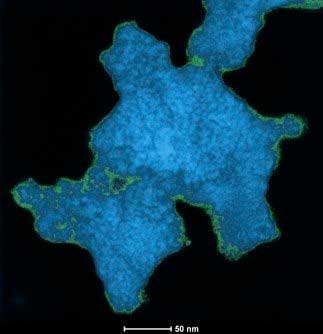
electron microscopy of cross-linked titania nanoparticles with boron-based clusters
This shows electron microscopy of cross-linked titania nanoparticles with boron-based clusters. Argonne researchers helped create a method to build these networks. (Image: Alexander Spokoyny, UCLA)
Metal oxides are of interest to scientists because of their unique electronic and chemical properties. Some, like titanium dioxide, are commonly used in photovoltaic and photocatalytic applications because of their ability to absorb light.
The key to forming these metal oxide networks is boron, which when annealed with metal oxides leads to the formation of thermally robust and stable interconnected clusters that act as strands of glue that connect a metal oxide web.
“This glue has the ability to be a key component of the entire reactive system, changing the properties that the metal oxides had on their own,” said Alexander Spokoyny, a chemist at UCLA.
The formation of the boron-metal oxide network provides a launching point for future studies of different materials that could combine their own natural properties with the added advantage of a similar “cross-linked” structure.
“We want to know, for instance, if we can transfer our knowledge of this mesh to a material like silicon dioxide. The photocatalytic properties of these materials are extraordinary compared to titanium dioxide,” said Argonne chemist Max Delferro.
In the future, the researchers seek to design a way to create precisely tailored materials by perfecting how the interconnecting clusters of boron “glue” are interspersed within the metal oxide. “If we can stitch in these molecules exactly where we want them to be, it will give us a powerful ability to make and understand hybrid materials with a wide range of uses,” Spokoyny said.
Because these materials are so new, the researchers believe they have a great deal of untapped potential. “We’re not claiming mission fully accomplished by any means; there are still parts of the chemistry that we don’t fully understand and appreciate,” Delferro said.
The research team included Argonne chemist Karena Chapman, who works at the laboratory’s Advanced Photon Source (APS), a DOE Office of Science User Facility. Chapman and Spokoyny met when they were named to Chemical and Engineering News’s “Talented Twelve” list in 2016, and established the collaboration that led to the research.
According to Chapman, a member of the Structural Sciences Group in the APS X-ray Science division, the structural characterization of the material involved the use of X-ray pair distribution function analysis carried out at the APS, which gives local structural information about the relative atom positions.
Chapman, Delferro and Spokoyny noted that the efforts of the research team to produce and analyze this new material were just as interconnected as the discovered hybrid material itself. “There are cross-linkages at both the molecular and the human level,” Delferro said. “This work proves that we work better and are stronger when we’re connected.”
Source: Argonne National Laboratory