Clasa nouă de materiale: Izolatori topologici de înaltă calitate;o nouă clasă de izolatori topologici care au proprietăți de conducere pe marginea cristalelor, mai degrabă decât pe suprafața lor;Cercetatorii spera ca in viitor nanofirele fabricate din izolatii topologice de ordin superior pot fi folosite ca trasee de conducere in circuitele electrice. Acestea ar putea fi combinate cu materiale magnetice și superconductoare și utilizate pentru construirea calculatoarelor cuantice.
Posted: Jun 01, 2018
Novel insulators with conducting edges
(Nanowerk News) Topology examines the properties of objects and solids that are protected against perturbations and deformations. Materials known so far include topological insulators, which are crystals that insulate on the inside but conduct electrical current on their surface. The conducting surfaces are topologically protected, which means that they cannot easily be brought into an insulating state.
New class of materials: Higher-order topological insulators
Theoretical physicists at the University of Zurich have now predicted a new class of topological insulators that have conducting properties on the edges of crystals rather than on their surface.
The research team, made up of scientists from UZH, Princeton University, the Donostia International Physics Center and the Max Planck Institute of Microstructure Physics in Halle, dubbed the new material class „higher-order topological insulators” (Science Advances, „Higher-order topological insulators”).
This is a schematic of a higher-order topological insulator in the shape of a nanowire, with conducting channels on its edges. (Image: University of Zurich)
The extraordinary robustness of the conducting edges makes them particularly interesting: The current of topological electrons cannot be stopped by disorder or impurities. If an imperfection gets in the way of the current, it simply flows around the impurity.
Like a highway for electrons
In addition, the crystal edges do not have to be specially prepared to conduct electrical current. If the crystal breaks, the new edges automatically also conduct current.
„The most exciting aspect is that electricity can at least in theory be conducted without any dissipation,” says Titus Neupert, professor at the Department of Physics at UZH. „You could think of the crystal edges as a kind of highway for electrons. They can’t simply make a U-turn.”
This property of dissipationless conductance, otherwise known from superconductors at low temperatures, is not shared with the previously known topological insulator crystals that have conducting surfaces, but is specific to the higher-order topological crystals.
Further theoretical and experimental research needed
The physicists’ study still mostly relies on theoretical aspects. They have proposed tin telluride as the first compound to show these novel properties. „More material candidates have to be identified and probed in experiments,” says Neupert.
The researchers hope that in the future nanowires made of higher-order topological insulators may be used as conducting paths in electric circuits. They could be combined with magnetic and superconducting materials and used for building quantum computers.
Pistoalele și revistele 590M sunt proiectate în mod unic, încorporând nervuri de stabilizare care angajează magazia direct la receptor pentru o blocare sigură. Seria 590M ™ oferă comoditate alimentată de magazine în legendara platformă tactică Mossberg cu pompă de acțiune.
Pentru aplicații de securitate la domiciliu, tactică și de competiție, acțiunile pompelor 590M Mag-Fed oferă multe avantaje practice: reîncărcarea / descărcarea mai rapidă, creșterea capacității fără o lungime suplimentară a tubului de revistă și trecerea rapidă și ușoară între diferite tipuri de încărcături ).
Mossberg 590M Heat Shield Mag-Fed Pump-Action Combat/Tactical Shotgun: Up to 20 rounds of 12-Gauge Firepower, and Quick Full-Capacity Reloads! (Videos!)
DefenseReview (DR) has always been a big fan of combat/tactical shotguns, particularly for home defense. However, we weren’t really properly trained in their use until Steve Fisher of Sentinel Conceptstaught us the right way to run a combat shotgun competently at Beretta Tactical Summit 2015. The course was a real eye opener, and made us much more confident in choosing a shotgun for certain dynamic CQB/CQC (Close Quarters Battle/Close Quarters Combat) gunfighting scenarios, like home defense, for example. Well, American heritage company Mossberg’s developed two shotguns that may just be the ultimate pump-action combat shotguns in the world, the Mossberg 590M Mag-Fed Shotgun and Mossberg 590M Heat Shield Mag Fed Shotgun.
Both Mossberg 590M Mag-Fed Shotguns will give you up to 20-rounds of 12-Gauge firepower and very fast full-capacity reloads to deal with whatever problem you’ve got. The only difference is that the Mossberg 590M Heat Shield Mag-Fed pump-action shotgun also gives you a nice-looking and functional perforated steel heat shield over the barrel, ghost ring combat sights (iron sights), and a “Tri-Rail” Mil-Std-1913 “Picatinny” rail underneath the pump-action grip, in case you want to mount a vertical fore grip. DR’s only concern with this last feature is that it might cause the pumping hand some discomfort, so we’d have to test it at the range. Other than than one question mark, the Heat Shield model is our current favorite, and it looks cooler.
For home defense, the Mossberg 590M Mag-Fed Shotguns are formidable, and there’s frankly nothing better that that loud pumping action to scare off an inttruder and would-be burglar before you actually have to shoot them in self defense. We’re not saying it’s a surefire deterrent, but it’s the best one we know, especially inside a structure, where sound is contained and magnified.
The Mossberg 590M Mag-Fed Shotgun mags (box magazines) are available in 5, 10, 15 and 20-round capacities, and Mossberg says that the mags will fit inside 7.62mm NATO (7.62x51mm NATO)/.308 Win. double-mag pouches.
Assuming they work as advertised and prove reliable, accurate and durable, Defense Review really digs these shotguns, and can’t wait to try them out at the range.
The following information on the Mossberg 590M Mag-Fed Shotguns comes from the company’s website:
“590M® Mag-Fed
RELOADING & UNLOADING CONVENIENCE USING COMPACT, INTERCHANGEABLE MAGAZINES
590M shotguns and magazines are uniquely designed incorporating stabilizing ribs that engage the magazine directly to the receiver for a sure lock-up. The 590M™ Series offers magazine-fed convenience in the legendary Mossberg pump-action tactical platform.
For home security, tactical, and competition applications, 590M Mag-Fed pump-actions offer many practical advantages: faster reloading/unloading, increased capacity without additional magazine tube length, and quick and easy transitioning between various types of loads (when using designated magazines).
Full magazines are the center of gravity point, making the 590M shotgun easy to balance for greater accuracy. The 590M is designed around the Mossberg 590,® the choice of tactical users worldwide and time-tested over decades of dependable service.
The features Mossberg tactical pump users expect are all there: Dual extractors, Twin action bars, Positive steel-to-steel lockup, Drilled and tapped receiver, Ambidextrous safety, and a Heavy-walled barrel.
590M Accessory magazines are available in 5,10,15 and 20 shot capacity.
World’s First Double-Stack Shotgun Magazine Design 590M magazine’s patented design provides more capacity in less magazine length than competitor’s single stack designs. Offered in four capacities: 20, 15, 10 and 5-Round.
All-steel magazine release button and housing is optimally positioned in front of the trigger guard for quick, ambidextrous access for reloading — and will not interfere with cycling the action.
590M shotguns and magazines are uniquely designed incorporating stabilizing ribs that engage the magazine directly to the receiver for a sure lock-up.
590M™ SERIES ACCESSORY MAGAZINES PACK MORE ROUNDS INTO SHORTER MAGAZINES — QUICKLY AND EFFICIENTLY ADDING CAPACITY.
The world’s first production double-stack 12GA shotgun magazine offers a shorter magazine length vs. capacity than competitor’s single-stack designs, providing better swing, balance and control.
Magazine construction highlights: Hardened steel feed lips, over-molded steel shell ramps, easy-grip external molded design, proprietary self-lubricating polymer magazine body material, heavy-duty ASTM-A-228 music wire magazine spring, removable floor plate for easy cleaning, and a tough black oxide finish on steel components.
For shooting flexibility, 590M magazines are available in 5, 10, 15, and 20-Round, and are for use with 2.75” shotshells.
Hardened steel feed lips and over-molded steel shell ramps ensure efficient feeding. Anti-cant rounded follower improves feeding; round limiter improves spring life.
Removable floor plate for easy cleaning; ASTM-A-228 music wire springs improve feeding, increase durability, and prolong service life.“
UAV-urile sunt un schimbător de joc pentru Armata Australiană, oferind o conștientizare situațională sporită pentru o execuție mai bună a misiunii pentru soldați.
Dioxidul de vanadiu (VO 2 ) este un astfel de material. Se poate trece de la o fază izolatoare la o fază metalică chiar deasupra temperaturii camerei, o caracteristică exploatată deja pentru senzori.Privind materialul cu o rezoluție de 50 nm, oamenii de știință au putut observa că defectele din material au jucat un rol important în inițierea tranziției de fază de la izolator la metal. Cu toate acestea, mai important, autorii au observat de asemenea o a treia stare intermediară formată în timpul transformării de fază.
Posted: May 30, 2018
Insulator-metal transition at the nanoscale
(Nanowerk News) Controlling the flow of electrons within circuits is how electronic devices work. This is achieved through the appropriate choice of materials. Metals allow electrons to flow freely and insulators prevent conduction. In general, the electrical properties of a material are determined when the material is fabricated and cannot be changed afterwards without changing the material.
However, there are materials that can exhibit metal or insulator behaviour depending on their temperature. Being able switch their properties, these materials could lead to a new generation of electronic devices.
Vanadium Dioxide (VO2) is one such material. It can switch from an insulating phase to a metallic phase just above room temperature, a feature exploited already for sensors. However, the reason why the properties of this material change so dramatically has been a matter of scientific debate for over 50 years.
One of the challenges in understanding why and how this switch occurs is due to a process called phase separation. The insulator-metal phase transition is similar to the ice to liquid transition in water. When ice melts, both liquid and solid water can coexist in separate regions.
Similarly, in VO2, insulating and metallic regions of the material can be coexisting at the same time during the transition. But unlike water, where the different regions are often large enough to see with the naked eye, in VO2 this separation occurs on the nanoscale and it is thus challenging to observe.
As a result, it has been hard to know if the true properties of each phase, or the mixture of both phases, are being measured.
X-rays are a key tool for understanding the properties of materials, but it has been hard to use them to probe materials on the nanoscale because it is hard to build lenses for microscopes that can detect them.
This technique is capable of imaging the electronic and structural changes in this material with an unprecedented resolution at the nanoscale without the need of a lens.
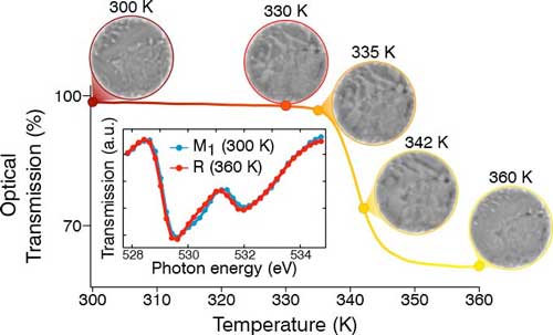
Phase transition from insulator to metallic phase in VO2 as a function of the temperature. (Image: ICFO)
By looking at the material with 50 nm resolution, the scientists were able to observe that defects in the material played an important role in initiating the phase transition from the insulator to the metal. However, more importantly, the authors also observed a third intermediate state formed during the phase transformation.
Whilst some regions transformed directly from the insulating to metallic phase, others transformed into a second different insulating state before becoming metallic at higher temperatures with the exact pathway taken depending on the defects present in the material.
The coexistences of three phases has radically changed the views of previous studies that assumed the presence of only two states during the transition. Even more, the study presents new ways in which the transition could be controlled.
In addition to the results obtained on the phase transition in VO2, the work also highlights the possibilities that X-ray holography can bring for studying materials on the nanoscale.
The technique is the only method that can image real-time nanoscale dynamics and is now being used to study the properties of other intriguing materials such as high temperature superconductors.
Nanoscientii de la Universitatea Northwestern au dezvoltat un plan pentru fabricarea de noi heterostructuri din diferite tipuri de materiale 2-D. Materialele 2-D sunt straturi individuale de atomi care pot fi stivuite împreună ca „blocuri de construcție nano-interblocate”. Materialele de știință și fizicienii sunt încântați de proprietățile materialelor 2-D și de aplicațiile lor potențiale.
Posted: May 30, 2018
Building nanomaterials for next-generation computing
(Nanowerk News) Nanoscientists at Northwestern University have developed a blueprint to fabricate new heterostructures from different types of 2-D materials. 2-D materials are single atom layers that can be stacked together like “nano-interlocking building blocks.” Materials scientists and physicists are excited about the properties of 2-D materials and their potential applications. The researchers describe their blueprint in the Journal of Applied Physics(„Controlled synthesis of 2D MX2 (M=Mo, W; X=S, Se) heterostructures and alloys”).
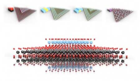
Top: Vertical MoSe2-WSe2 heterostructure, radial MoS2-WS2 heterostructure, hybrid MoS2-WS2heterostructure and MoSe2-WSe2 alloy building block representations and crystal structure models; Bottom: Vertical MoSe2-WSe2 heterostructure crystal structure model(Image: Cain, Hanson and Dravid)
“We’ve outlined an easy, deterministic and readily deployable way to stack and stitch these individual layers into orders not seen in nature,” said Jeffrey Cain, an author on the paper who was formerly at Northwestern University but is now at Lawrence Berkeley National Laboratory and the University of California.
Cain explained that for nanoscientists, “the dream” is to combine 2-D materials in any order and collate a library of these heterostructures with their documented properties. Scientists can then select appropriate heterostructures from the library for their desired applications. For instance, the computer industry is trying to make transistors smaller and faster to increase computing power. A nanoscale semiconductor with favorable electronic properties could be used to make transistors in next-generation computers.
So far, nanoscientists have lacked clear methods for fabricating heterostructures, and have not yet been able to develop this library. In this work, the scientists looked to solve these fabrication issues. After identifying trends in the literature, they tested different conditions to map out the different parameters required to grow specific heterostructures from four types of 2-D materials: molybdenum disulfide and diselenide, and tungsten disulfide and diselenide. To fully characterize the atomically thin final products, the scientists used microscopy and spectrometry techniques.
The group was inspired by the science of time-temperature-transformation diagrams in classical materials, which maps out heating and cooling profiles to generate precise metallic microstructures. Based on this method, the researchers packaged their findings into one diagrammatic technique – the Time-Temperature-Architecture Diagram.
“People had previously written papers for specific morphologies, but we have unified it all and enabled the generation of these morphologies with one technique,” Cain said.
The unified Time-Temperature-Architecture Diagrams provide directions for the exact conditions required to generate numerous heterostructure morphologies and compositions. Using these diagrams, the researchers developed a unique library of nanostructures with physical properties of interest to physicists and materials scientists. The Northwestern University scientists are now examining the behaviors displayed by some materials in their library, like the electron flow across the stitched junctions between materials.
The researchers hope that their blueprint design will be useful for heterostructure fabrication beyond the first four materials. “Our specific diagrams would need revisions in the context of each new material, but we think that this idea is applicable and extendable to other material systems,” Cain said.
Cercetatorii care lucreaza la Laboratorul National Lawrence Berkeley din cadrul Departamentului de Energie (Berkeley Lab) au un cuplu de grafen, o forma monostrat de carbon, cu straturi subtiri de materiale magnetice cum ar fi cobalt si nichel pentru a produce comportament exotic in electroni. – aplicații de calcul de generare.De obicei, cercetătorii care lucrează pentru a produce acest comportament pentru electronii din materiale au cuplat metale grele și scumpe precum platina și tantalul cu materiale magnetice pentru a obține astfel de efecte, dar grafenul oferă o alternativă potențial revoluționară, deoarece este ultrathin, ușor, are o conductivitate electrică foarte ridicată, și poate servi și ca strat protector pentru materiale magnetice predispuse la coroziune.
Posted: May 29, 2018
Graphene layered with magnetic materials could drive ultrathin spintronics
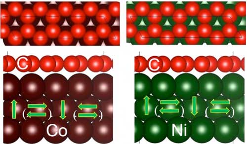
(Nanowerk News) Researchers working at the Department of Energy’s Lawrence Berkeley National Laboratory (Berkeley Lab) coupled graphene, a monolayer form of carbon, with thin layers of magnetic materials like cobalt and nickel to produce exotic behavior in electrons that could be useful for next-generation computing applications.
The work was performed in collaboration with French scientists including Nobel Laureate Albert Fert, an emeritus professor at Paris-Sud University and scientific director for a research laboratory in France. The team performed key measurements at Berkeley Lab’s Molecular Foundry, a DOE Office of Science User Facility focused on nanoscience research.
Fert shared the Nobel Prize in Physics in 2007 for his work in understanding a magnetic effect in multilayer materials that led to new technology for reading data in hard drives, for example, and gave rise to a new field studying how to exploit and control a fundamental property known as „spin” in electrons to drive a new type of low-energy, high-speed computer memory and logic technology known as spintronics.
In these images developed using the SPLEEM instrument at Berkeley Lab, the orientation of magnetization in samples containing cobalt (Co) and ruthenium (Ru) is represented with white arrows. The image at left shows how the orientation is altered when a layer of graphene (“Gr”) is added. The scale bar at the lower right of both images is 1 micron, or 1 millionths of a meter. (Image: Berkeley Lab)
The researchers found that the material’s electronic and magnetic properties create tiny swirling patterns where the layers meet, and this effect gives scientists hope for controlling the direction of these swirls and tapping this effect for a form of spintronics applications known as „spin-orbitronics” in ultrathin materials. The ultimate goal is to quickly and efficiently store and manipulate data at very small scales, and without the heat buildup that is a common hiccup for miniaturizing computing devices.
Typically, researchers working to produce this behavior for electrons in materials have coupled heavy and expensive metals like platinum and tantalum with magnetic materials to achieve such effects, but graphene offers a potentially revolutionary alternative since it is ultrathin, lightweight, has very high electrical conductivity, and can also serve as a protective layer for corrosion-prone magnetic materials.
„You could think about replacing computer hard disks with all solid state devices – no moving parts – using electrical signals alone,” said Andreas Schmid, a staff scientist at the Molecular Foundry who participated in the research. „Part of the goal is to get lower power-consumption and non-volatile data storage.”
The latest research represents an early step toward this goal, Schmid noted, and a next step is to control nanoscale magnetic features, called skyrmions, which can exhibit a property known as chirality that makes them swirl in either a clockwise or counterclockwise direction.
In more conventional layered materials, electrons traveling through the materials can act like an „electron wind” that changes magnetic structures like a pile of leaves blown by a strong wind, Schmid said.
But with the new graphene-layered material, its strong electron spin effects can drive magnetic textures of opposite chirality in different directions as a result of the “spin Hall effect,” which explains how electrical currents can affect spin and vice versa. If that chirality can be universally aligned across a material and flipped in a controlled way, researchers could use it to process data.
“Calculations by other team members show that if you take different magnetic materials and graphene and build a multilayer stack of many repeating structures, then this phenomenon and effect could possibly be very powerfully amplified,” Schmid said.
To measure the layered material, scientists applied spin-polarized low-energy electron microscopy (SPLEEM) using an instrument at the Molecular Foundry’s National Center for Electron Microscopy. It is one of just a handful of specialized devices around the world that allow scientists to combine different images to essentially map the orientations of a sample’s 3-D magnetization profile (or vector), revealing a its „spin textures.”
The research team also created the samples using the same SPLEEM instrument through a precise process known as molecular beam epitaxy, and separately studied the samples using other forms of electron-beam probing techniques.
Gong Chen, a co-lead author who participated in the study as a postdoctoral researcher at the Molecular Foundry and is now an assistant project scientist in the UC Davis Physics Department, said the collaboration sprang out of a discussion with French scientists at a conference in 2016 – both groups had independently been working on similar research and realized the synergy of working together.
While the effects that researchers have now observed in the latest experiments had been discussed decades ago in previous journal articles, Chen noted that the concept of using an atomically thin material like graphene in place of heavy elements to generate those effects was a new concept.
„It has only recently become a hot topic,” Chen said. „This effect in thin films had been ignored for a long time. This type of multilayer stacking is really stable and robust.”
Using skyrmions could be revolutionary for data processing, he said, because information can potentially be stored at much higher densities than is possible with conventional technologies, and with much lower power usage.
Molecular Foundry researchers are now working to form the graphene-magnetic multilayer material on an insulator or semiconductor to bring it closer to potential applications, Schmid said.
Cercetările conduse de oamenii de știință de la Universitatea din Luxemburg au arătat potențialul cojilor de cristal lichid ca materiale care permit o gamă largă de aplicații viitoare, de la tehnologia autoturismului până la tehnologia anti-contrafacere și o nouă clasă de senzori.Învelișurile de cristal lichid, numai fracții de un milimetru, astfel încât acestea să poată fi aplicate cu ușurință pe suprafețe, au câteva proprietăți unice care ar putea fi utilizate în inginerie: întrucât reflectă foarte selectiv lumina, ele pot fi aranjate în modele care pot fi citite pentru mașini, asemănător unui cod QR, adăugând informații codate obiectelor. „Aceste modele ar putea fi utilizate pentru a ghida vehicule autonome sau pentru a instrui roboții atunci când manipulează piesele dintr-o fabrică. Acest lucru ar putea deveni important mai ales în cazul aplicațiilor în interior unde dispozitivele GPS nu funcționează”, explică Prof. Lagerwall.
Posted: May 29, 2018
‘Smart’ material enables novel applications in autonomous driving and robotics
(Nanowerk News) Research led by scientists from the University of Luxembourg has shown the potential of liquid crystal shells as enabling material for a vast array of future applications, ranging from autonomous driving to anti-counterfeiting technology and a new class of sensors.
Liquid Crystals, already widely used in flat-screen TVs, are materials that are in a state between solid and liquid. Prof Jan Lagerwall and his team at the Physics and Materials Science Research Unit (PHYMS) at the University of Luxembourg have been investigating the unique mechanical and optical properties of microscopic shells that are produced of liquid crystal for several years.
Now, in a multidisciplinary collaboration with IT scientists Dr. Gabriele Lenzini and Prof Peter Ryan of the University’s Interdisciplinary Center for Security and Trust (SnT) as well as Mathew Schwartz, Assistant Professor at the New Jersey Institute of Technology, they published a report in the scientific journal Advanced Materials („Cholesteric Liquid Crystal Shells as Enabling Material for Information-Rich Design and Architecture”) describing potentially groundbreaking future applications for the material.
Liquid Crystal shells, only fractions of a millimeter in size so they can easily be applied to surfaces, have several unique properties that could be utilized in engineering: As they reflect light highly selectively, they can be arranged into patterns that are readable for machines, akin to a QR code, adding coded information to objects. „These patterns could be used to guide autonomous vehicles or to instruct robots when handling workpieces in a factory. This could become important especially in indoors applications where GPS devices don’t work,” Prof Lagerwall explains.
The shells can be manufactured to reflect only certain wavelengths of light, such as infrared, that would be invisible to the human eye. As the Liquid Crystal shells reflect light „omnidirectionally” meaning that beholders see the same pattern regardless of their position and viewing angle, the patterns can even be read by moving objects.
Additionally, the shells can be manufactured in a way that they change their structure when they are exposed to certain external impacts, such as pressure, heat or specific chemicals.
Together with computers to interpret these changes, the shells could be used as sensors, for example as pressure sensors in the fingertips of robots enabling tactile feeling which is currently hard to achieve in robotic engineering. Another application could be fire exit signage on walls inside buildings that only becomes visible when the temperature exceeds a certain threshold. The big advantage of these sensors is that they passively react to external impacts and don’t need electricity and batteries.
Finally, liquid crystal shells could be used to prevent counterfeiting. The micropatterns that emerge when the shells are brought together are unique and impossible to copy. These unclonable patterns could be used to create uncopiable identifiers that can be attached to valuable objects, such as art works or expensive pharmaceuticals. In combination with cryptographic tools they could be used to create a system that ensures that a buyer or user has the original and not a counterfeited product.
Prof Lagerwall makes clear that the ideas outlined in the report require further research. „Our hope is that the article can stimulate future research on liquid crystalline materials into new directions that are in line with the current societal developments,” he said.
Apoi, astfel de fibre ar putea fi filetate în bandaje, împreună cu textile, cum ar fi îmbrăcămintea atletică și pantofii ca indicatori de culoare pentru, de exemplu, tulpina musculară în timpul antrenamentelor. Kolle prevede că acestea pot fi, de asemenea, utilizate ca senzori de tensiune pentru infrastructură și mașini.
(Nanowerk News) Compression therapy is a standard form of treatment for patients who suffer from venous ulcers and other conditions in which veins struggle to return blood from the lower extremities. Compression stockings and bandages, wrapped tightly around the affected limb, can help to stimulate blood flow. But there is currently no clear way to gauge whether a bandage is applying an optimal pressure for a given condition.
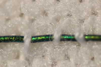
Now engineers at MIT have developed pressure-sensing photonic fibers that they have woven into a typical compression bandage. As the bandage is stretched, the fibers change color. Using a color chart, a caregiver can stretch a bandage until it matches the color for a desired pressure, before, say, wrapping it around a patient’s leg.
The photonic fibers can then serve as a continuous pressure sensor — if their color changes, caregivers or patients can use the color chart to determine whether and to what degree the bandage needs loosening or tightening.
“Getting the pressure right is critical in treating many medical conditions including venous ulcers, which affect several hundred thousand patients in the U.S. each year,” says Mathias Kolle, assistant professor of mechanical engineering at MIT. “These fibers can provide information about the pressure that the bandage exerts. We can design them so that for a specific desired pressure, the fibers reflect an easily distinguished color.”
Engineers at MIT have developed pressure-sensing photonic fibers that they have woven into a typical compression bandage. (Courtesy of the researchers)
Kolle and his colleagues have published their results in the journal Advanced Healthcare Materials(„Stretchable Optomechanical Fiber Sensors for Pressure Determination in Compressive Medical Textiles”). Co-authors from MIT include first author Joseph Sandt, Marie Moudio, and Christian Argenti, along with J. Kenji Clark of the Univeristy of Tokyo, James Hardin of the United States Air Force Research Laboratory, Matthew Carty of Brigham and Women’s Hospital-Harvard Medical School, and Jennifer Lewis of Harvard University.
Natural inspiration
The color of the photonic fibers arises not from any intrinsic pigmentation, but from their carefully designed structural configuration. Each fiber is about 10 times the diameter of a human hair. The researchers fabricated the fiber from ultrathin layers of transparent rubber materials, which they rolled up to create a jelly-roll-type structure. Each layer within the roll is only a few hundred nanometers thick.
In this rolled-up configuration, light reflects off each interface between individual layers. With enough layers of consistent thickness, these reflections interact to strengthen some colors in the visible spectrum, for instance red, while diminishing the brightness of other colors. This makes the fiber appear a certain color, depending on the thickness of the layers within the fiber.
“Structural color is really neat, because you can get brighter, stronger colors than with inks or dyes just by using particular arrangements of transparent materials,” Sandt says. “These colors persist as long as the structure is maintained.”
The fibers’ design relies upon an optical phenomenon known as “interference,” in which light, reflected from a periodic stack of thin, transparent layers, can produce vibrant colors that depend on the stack’s geometric parameters and material composition. Optical interference is what produces colorful swirls in oily puddles and soap bubbles. It’s also what gives peacocks and butterflies their dazzling, shifting shades, as their feathers and wings are made from similarly periodic structures.
“My interest has always been in taking interesting structural elements that lie at the origin of nature’s most dazzling light manipulation strategies, to try recreating and employing them in useful applications,” Kolle says.
A multilayered approach
The team’s approach combines known optical design concepts with soft materials, to create dynamic photonic materials.
While a postdoc at Harvard in the group of Professor Joanna Aizenberg, Kolle was inspired by the work of Pete Vukusic, professor of biophotonics at the University of Exeter in the U.K., on Margaritaria nobilis, a tropical plant that produces extremely shiny blue berries. The fruits’ skin is made up of cells with a periodic cellulose structure, through which light can reflect to give the fruit its signature metallic blue color.
Together, Kolle and Vukusic sought ways to translate the fruit’s photonic architecture into a useful synthetic material. Ultimately, they fashioned multilayered fibers from stretchable materials, and assumed that stretching the fibers would change the individual layers’ thicknesses, enabling them to tune the fibers’ color. The results of these first efforts were published in Advanced Materials in 2013.
When Kolle joined the MIT faculty in the same year, he and his group, including Sandt, improved on the photonic fiber’s design and fabrication. In their current form, the fibers are made from layers of commonly used and widely available transparent rubbers, wrapped around highly stretchable fiber cores. Sandt fabricated each layer using spin-coating, a technique in which a rubber, dissolved into solution, is poured onto a spinning wheel. Excess material is flung off the wheel, leaving a thin, uniform coating, the thickness of which can be determined by the wheel’s speed.
For fiber fabrication, Sandt formed these two layers on top of a water-soluble film on a silicon wafer. He then submerged the wafer, with all three layers, in water to dissolve the water-soluble layer, leaving the two rubbery layers floating on the water’s surface. Finally, he carefully rolled the two transparent layers around a black rubber fiber, to produce the final colorful photonic fiber.
Reflecting pressure
The team can tune the thickness of the fibers’ layers to produce any desired color tuning, using standard optical modeling approaches customized for their fiber design.
“If you want a fiber to go from yellow to green, or blue, we can say, ‘This is how we have to lay out the fiber to give us this kind of [color] trajectory,’” Kolle says. “This is powerful because you might want to have something that reflects red to show a dangerously high strain, or green for ‘ok.’ We have that capacity.”
The team fabricated color-changing fibers with a tailored, strain-dependent color variation using the theoretical model, and then stitched them along the length of a conventional compression bandage, which they previously characterized to determine the pressure that the bandage generates when it’s stretched by a certain amount.
The team used the relationship between bandage stretch and pressure, and the correlation between fiber color and strain, to draw up a color chart, matching a fiber’s color (produced by a certain amount of stretching) to the pressure that is generated by the bandage.
To test the bandage’s effectiveness, Sandt and Moudio enlisted over a dozen student volunteers, who worked in pairs to apply three different compression bandages to each other’s legs: a plain bandage, a bandage threaded with photonic fibers, and a commercially-available bandage printed with rectangular patterns. This bandage is designed so that when it is applying an optimal pressure, users should see that the rectangles become squares.
Overall, the bandage woven with photonic fibers gave the clearest pressure feedback. Students were able to interpret the color of the fibers, and based on the color chart, apply a corresponding optimal pressure more accurately than either of the other bandages.
The researchers are now looking for ways to scale up the fiber fabrication process. Currently, they are able to make fibers that are several inches long. Ideally, they would like to produce meters or even kilometers of such fibers at a time.
“Currently, the fibers are costly, mostly because of the labor that goes into making them,” Kolle says. “The materials themselves are not worth much. If we could reel out kilometers of these fibers with relatively little work, then they would be dirt cheap.”
Then, such fibers could be threaded into bandages, along with textiles such as athletic apparel and shoes as color indicators for, say, muscle strain during workouts. Kolle envisions that they may also be used as remotely readable strain gauges for infrastructure and machinery.
“Of course, they could also be a scientific tool that could be used in a broader context, which we want to explore,” Kolle says.
Oamenii de stiinta de la universitatile din Cambridge si Bristol au gasit o modalitate de a crea nanostructuri din material plastic semiconductoare care absorb lumina si transportul energiei sale de 20 de ori mai mult decat a fost observat anterior, deschizand calea pentru celulele solare mai flexibile si mai eficiente si fotodetectori .Echipa de cercetare planifică acum să pregătească structuri mai groase decât cele din studiul actual și mai mare decât adâncimea de absorbție optică, în vederea construirii prototipului de celule solare bazate pe această tehnologie.
Ele pregătesc și alte structuri capabile să utilizeze lumina pentru a efectua reacții chimice, cum ar fi împărțirea apei în hidrogen și oxigen
Posted: May 29, 2018
Plastic crystals hold key to record-breaking energy transport
(Nanowerk News) Scientists from the Universities of Cambridge and Bristol have found a way to create plastic semiconductor nanostructures that absorb light and transport its energy 20 times further than has been previously observed, paving the way for more flexible and more efficient solar cells and photodetectors.
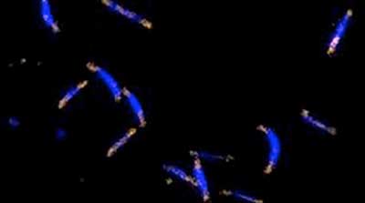
Image showing light emission from the polymeric nanostructures and schematic of a single nanostructure. (Image: University of Bristol)
Lightweight semiconducting plastics are now widely used in mass market electronic displays such as those found in phones, tablets and flat-screen televisions. However, using these materials to convert sunlight into electricity to make solar cells is far more complex.
The photo-excited states – when photons of light are absorbed by the semiconducting material – need to move so that they can be “harvested” before they lose their energy. These excitations typically only travel about 10 nanometres in plastic (or polymeric) semiconductors, so researchers need to build tiny structures patterned at the nanoscale to maximise the “harvest”.
Dr Xu-Hui Jin and colleagues at the University of Bristol developed a new way to make highly ordered crystalline semiconducting structures using polymers.
Dr Michael Price of Cambridge’s Cavendish Laboratory measured the distance that the photo-exited states travelled, which reached distances of 200 nanometres – 20 times further than was previously possible.
200 nanometres is especially significant because it is greater than the thickness of material needed to completely absorb ambient light, making these polymers more suitable as “light harvesters” for solar cells and photodetectors.
“The gain in efficiency would actually be for two reasons: first, because the energetic particles travel further, they are easier to “harvest”, and second, we could now incorporate layers around 100 nanometres thick, which is the minimum thickness needed to absorb all the energy from light – the so-called optical absorption depth,” said co-author Dr George Whittell from the University of Bristol. “Previously, in layers this thick, the particles were unable to travel far enough to reach the surfaces.”
“The distance that energy can be moved in these materials comes as a big surprise and points to the role of unexpected quantum coherent transport processes,” said co-author Professor Sir Richard Friend from Cambridge’s Cavendish Laboratory, and a Fellow of St John’s College.
The research team now plans to prepare structures thicker than those in the current study and greater than the optical absorption depth, with a view to building prototype solar cells based on this technology.
They are also preparing other structures capable of using light to perform chemical reactions, such as the splitting of water into hydrogen and oxygen.