Nanoparticulele polimerice fluorescente îndreaptă degetul spre urme de dispozitive explozive (Fluorescent polymer nanoparticles point the finger at traces of explosive devices )

Loturile de bombe ar putea fi contracarate cu ajutorul unui sistem portabil pentru detectarea urmelor de explozivi exploziva folosind nanoparticule polimerice fluorescente, dezvoltat de A * STAR. Imprimate pe hârtie, acești polimeri prezintă o performanță de detecție a explozivului mult mai robustă decât materialele anterioare cu proprietăți similare ( Polymer Chemistry , poli (trifenil ethene) și poli (tetraphenyl ethene): sinteza, proprietatea de emisie indusă de agregare și aplicarea ca hârtie senzori pentru detectarea efectivă a nitro-compușilor ” ).
Multe metode au fost dezvoltate pentru a detecta urme de explozivi de mare intensitate, cum ar fi trinitrotoluenul (TNT), dar majoritatea necesită instrumente analitice de laborator, cum ar fi detectorii de absorbție UV sau spectrometrele de masă, spune Jianwei Xu de la Institutul A * Engineering, care a condus lucrarea. „Ne-am propus să dezvoltăm o alternativă portabilă, rapidă, ieftină și foarte sensibilă”.

Posted: Sep 08, 2017

Fluorescent polymer nanoparticles point the finger at traces of explosive devices

(Nanowerk News) Bomb plots could be thwarted with the help of a portable system for detecting traces of high explosives using fluorescent polymer nanoparticles, developed by A*STAR. Coated on to paper, these polymers display an explosive-detection performance far more robust than previous materials with similar properties (Polymer Chemistry, „Poly(triphenyl ethene) and poly(tetraphenyl ethene): synthesis, aggregation-induced emission property and application as paper sensors for effective nitro-compounds detection”).

Many methods have been developed to detect traces of high explosives such as trinitrotoluene (TNT), but most require large, lab-based analytical instruments such as UV absorption detectors or mass spectrometers, says Jianwei Xu from the A*STAR Institute of Materials Research and Engineering, who led the work. “We aimed to develop a portable, quick, inexpensive and highly sensitive alternative.”
polymer-coated polymer readily could detect fingerprints contaminated with traces of four common high explosives
The polymer-coated polymer readily could detect fingerprints contaminated with traces of four common high explosives, including TNT.
Xu focused on fluorescent polymers whose light emission dims when exposed to vapors of molecules such as TNT that contain ‘nitro-groups’ — the nitrogen-rich structure that give high explosives their energetic properties.
Although explosive-detecting fluorescent polymers have been developed before, there have been obstacles to their practical use, Xu explains. Some lost part of their fluorescence in solid form through a process called aggregation-caused quenching. Others lacked the necessary porosity for explosives vapor penetration, only retaining an effective response when formed in layers of around 2.5 nanometers — so thin, the sensor would be very difficult to fabricate cheaply.
Xu and his colleagues have been developing polymers that, rather than losing their light emission in the solid state, become brighter, an effect known as aggregation-induced emission (AIE). “Our previous research demonstrated that porous films obtained from AIE active copolymers show a strong response to the vapor of nitro-compounds,” says Xu.
The team has now developed two new polymers, poly(triphenyl ethene) (PTriPE) and poly (tetraphenyl ethene) (PTPE), designed to maximize AIE, porosity and nitro group sensitivity. The polymers’ multiple bulky phenyl groups help keep them rigid and maximize light emission following aggregation. But in the presence of nitro-groups, electron transfer between polymer and analyte rapidly quenches the light.
“Paper sensors fabricated by absorbing the polymer nanoparticles on to filter paper showed high sensitivity for nitro-compound particles,” says Xu. PTriPE proved to be the pick of the pair, detecting TNT at a concentration of five parts per billion, even in polymer layers 1000 nanometers thick.
“This technology could be used at airports, ports and for border control for detecting explosives in any explosive-contaminated containers, clothing, boxes or bags,” says Xu. “We are seeking co-operation with industry to commercialize this technology.”
Source: A*STAR

Read more: Fluorescent polymer nanoparticles point the finger at traces of explosive devices

Cum pot fi direcționate bolile folosind nanotehnologia – și de ce este dificil( How diseases can be targeted using nanotechnology – and why it’s difficult)

anticorpul corect. Un antigen este legat de un anticorp. (Imagine: © ACS, Autor furnizat)
Aceste tipuri de nanoparticule pot funcționa bine în laborator, dar atunci când sunt utilizate în medii biologice mai complexe (cum ar fi în sânge, mai degrabă decât în ​​soluție tampon de sare), lucrurile devin rapid mai complicate.
De exemplu, atunci când nanoparticulele sunt injectate în sânge, proteinele se adsorb pe suprafața lor și acest lucru își poate schimba comportamentul complet ( Chem. , Rev. , „Corona biomoleculelor nanoparticule: lecții învățate – provocare acceptată?” ). Acest lucru se datorează faptului că această acoperire bio schimbă proprietățile importante ale particulelor, incluzând încărcarea (pozitivă, neutră sau negativă) și mărimea.Nanomaterialele administrate la o experiență de șoarece au multe niveluri diferite de complexitate biologică. Toate acestea trebuie luate în considerare la proiectarea nanomedicinei.

Posted: Sep 08, 2017

How diseases can be targeted using nanotechnology – and why it’s difficult

(Nanowerk News) Scientists are designing materials that are a thousand times smaller than the width of a hair. Known as nanomaterials or nanoparticles, some could help treat diseases.

However, the engineering of particles for biomedical applications remains challenging, particularly when moving from the test tube to biological environments.
This is an issue we discussed in a recent paper (Advanced Healthcare Materials, „Particle Targeting in Complex Biological Media”). A nanoparticle in the lab is one thing, but a nanoparticle interacting with blood, cells and tissues is another, and the behaviour of particles can change considerably when moving from one environment to another.
“Bio-nano interactions” are what govern these changes in behaviour, and this is a research area with plenty of difficulties, but also significant rewards.
layer-by-layer assembly - Using nanotechnology to prepare nanomaterials
Using nanotechnology to prepare nanomaterials. The example here is called layer-by-layer assembly. (© 2015 AAAS and 2016 ACS, Author provided)

Using nanoparticles to target diseases

Nanoparticles could help create more effective medical treatments. The aim is to improve areas ranging from drug delivery to the detection of diseases.
One of the potential benefits of nanoparticles is the possibility of developing targeted therapies, so that drugs go exactly where they are needed in the body.
For example, many highly effective chemo-therapeutics exist today, but because they do not interact only with cancer cells but with healthy ones too, many of them have side effects such as heart and bone marrow damage. This limits their efficacy and plays a big role in why treating cancer can be so difficult.

Why is targeting so hard?

But targeted drug therapies using nanoparticles also remain limited (ACS Central Science, „Does Nanomedicine Have a Delivery Problem?”). As in many other areas, what works in the laboratory can be difficult to translate into the clinic.
One example is the use of nanoparticles as “carriers” that are loaded with a drug and then accumulate at target cells (see image below).
Nanomaterials can be used to target specific cells
Nanomaterials can be used to target specific cells in the laboratory. In this image, they target/attach to the blue cells, but not to the green cells, and only when the correct antibody is used. An antigen is what an antibody binds to. (Image: © ACS, Author provided)
These types of nanoparticles can perform well in the laboratory, but when used in more complex biological environments (such as in blood rather than in salt buffer solution) things rapidly become more complicated.
For example, when nanoparticles are injected into blood, proteins adsorb onto their surface and this can completely change their behaviour (Chem. Soc. Rev., „The nanoparticle biomolecule corona: lessons learned – challenge accepted?”). This is because this bio-coating changes important properties of the particles, including charge (positive, neutral or negative) and size.

Possible solutions

New methods are being developed to evaluate nanoparticles in better ways. This includes investigative techniques that can complement cell and animal studies.
One example is microfluidic channels that can mimic blood vessels and can be used to study nanomaterial behaviour in blood capillaries.
Another option uses 3D printed tissues and organs. In one recent example, hydrogels filled with cells were printed onto a surface using a custom-built 3D printer.
The key point is to have adjustable complexity. That is, being able to adjust these methods so that we can get relevant and valuable information out of the studies. But not so complex that it becomes difficult to understand the mechanisms involved.
This is important, because a nanoparticle administered to an animal experiences several levels of biological complexity on its journey from the bloodstream to the target area (see image below). To understand fully what is happening, we need to study them all.
Nanomaterials administered to a mouse experience many different levels of biological complexity
Nanomaterials administered to a mouse experience many different levels of biological complexity. All of these need to be considered when designing nanomedicines. (Image: © ACS, Author provided)

Nanomedicines of tomorrow

The more we learn about bio-nano science – or how materials interact with biology on the nanoscale – the easier it will be to design nanoparticles that behave like we want them to.
After years of concerted efforts, a more clear picture of the mechanisms that determine how well a nanoparticle will work is emerging and the full extent of the challenge before us is starting to become clear.
It is unlikely that a single “quick fix” will be discovered.
Instead, research that manages to successfully combine ideas from different fields and researchers (JACS, „Increasing the Impact of Materials in and beyond Bio-Nano Science”) will likely lead to the development of new and improved targeted nanoparticles.
The aim is to provide new treatments for diseases that are difficult – or even impossible – to treat today.
Source: By Mattias Björnmalm, Marie Curie Research Fellow, Imperial College London and Frank Caruso, Professor and ARC Australian Laureate Fellow, University of Melbourne

Read more: How diseases can be targeted using nanotechnology – and why it’s difficult

Oamenii de știință dezvăluie noi perspective în materiale semiconductoare 2D promițătoare(Scientists unravel new insights into promising 2D semiconductor material )

au stabilit noi descoperiri cu privire la proprietatile disulfidului de molibden bidimensional (MoS 2 ), un semiconductor larg studiat al viitorului.MoS 2 – O alternativă la grafen
MoS 2 este un material semiconductor care prezintă proprietăți electronice și optice dorite pentru dezvoltarea și îmbunătățirea tranzistorilor, fotodetectoarelor și celulelor solare.structură similară cu MoS 2 .
„MoS 2 se încadrează într-un grup de materiale cunoscute sub numele de dihalcogenidele metalice de tranziție bidimensionale (2D-TMD) care prezintă un mare interes pentru cercetare din cauza potențialelor aplicații industriale. Noile cunoștințe din studiile noastre ne vor ajuta să deblocăm posibilitățile Aplicații bazate pe 2D-TMD, cum ar fi fabricarea de tranzistoare cu efect de câmp 2D-TMD „, a declarat Asst Prof Rusydi.
Folosind rezultatele acestor studii, cercetătorii vor aplica studii similare celorlalte 2D-TMD-uri și vor explora diferite posibilități de generare de proprietăți noi și valoroase în 2D-TMD care nu există în natură.

Posted: Sep 08, 2017

Scientists unravel new insights into promising 2D semiconductor material

(Nanowerk News) Researchers from the National University of Singapore (NUS) have established new findings on the properties of two-dimensional molybdenum disulfide (MoS2), a widely studied semiconductor of the future.

In two separate studies led by Professor Andrew Wee and Assistant Professor Andrivo Rusydi from the Department of Physics at the NUS Faculty of Science, the researchers uncovered the role of oxygen in MoS2, and a novel technique to create multiple tunable, inverted optical band gaps in the material. These novel insights deepen the understanding of the intrinsic properties of MoS2 which could potentially transform its applications in the semiconductor industry.
The studies were published in prestigious scientific journals Physical Review Letters and Nature Communications respectively.

MoS2 – An alternative to graphene

MoS2 is a semiconductor-like material that exhibits desirable electronic and optical properties for the development and enhancement of transistors, photodetectors and solar cells.
Prof Wee explained, „MoS2 holds great industrial importance. With an atomically thin two-dimensional structure and the presence of a 1.8eV energy band gap, MoS2 is a semiconductor that can offer broader applications than graphene which lacks a band gap.”

Presence of oxygen alters the electronic and optical properties of MoS2

In the first study published in Physical Review Letters on 16 August 2017 („Oxygen Passivation Mediated Tunability of Trion and Excitons in MoS2„), NUS researchers conducted an in-depth analysis which revealed that the energy storage capacity or dielectric function of MoS2 can be altered using oxygen.
The team observed that MoS2 displayed a higher dielectric function when exposed to oxygen. This new knowledge shed light on how adsorption and desorption of oxygen by MoS2 can be employed to modify its electronic and optical properties to suit different applications. The study also highlights the need for adequate consideration of extrinsic factors that may affect the properties of the material in future research.
The first author of this paper is Dr Pranjal Kumar Gogoi from the Department of Physics at NUS Faculty of Science.

MoS2 can possess two tunable optical band gaps

In the second study published in Nature Communications on 7 September 2017 („Tunable inverted gap in monolayer quasi-metallic MoS2 induced by strong charge-lattice coupling”), the team of NUS researchers discovered that as opposed to conventional semiconductors which typically have only one optical band gap, electron doping of MoS2 on gold can create two unusual optical band gaps in the material. In addition, the two optical bandgaps in MoS2 are tunable via a simple, straight forward annealing process.
The research team also identified that the tunable optical band gaps are induced by strong-charge lattice coupling as a result of the electron doping.
The first author of this second paper is Dr Xinmao Yin from the Department of Physics at NUS Faculty of Science.
The research findings from the two studies lend insights to other materials that possess similar structure with MoS2.
„MoS2 falls under a group of material known as the two-dimensional transitional metal dihalcogenides (2D-TMDs) which are of great research interest because of their potential industrial applications. The new knowledge from our studies will assist us in unlocking the possibilities of 2D-TMD-based applications such as the fabrication of 2D-TMD-based field effect transistors,” said Asst Prof Rusydi.
Leveraging the findings of these studies, the researchers will apply similar studies to other 2D-TMDs and to explore different possibilities of generating new, valuable properties in 2D-TMDs that do not exist in nature.
Source: National University of Singapore

Read more: Scientists unravel new insights into promising 2D semiconductor material

Evaluarea toxicității nanoclay(Assessing the toxicity of nanoclay)

„Modelul SAEC extinde impactul studiului nostru asupra unei platforme biologice mai umane, deoarece celulele primare imita mai mult țesutul lor de origine și reduc în continuare identificarea greșită, contaminarea, instabilitatea genetică generală și lipsa de funcții și markeri întâlnite adesea cu celulele imortalizate sisteme, „noteaza cercetatoriiCu o rată estimată de creștere de aproximativ 25% anual, nanocompozitele sau compozitele care conțin nanoclase încorporate în polimeri sunt de așteptat să aibă o largă implementare în produsele comerciale și industriale, de la materialele de ambalare pentru produsele alimentare la dispozitivele auto și medicale. În ambalajul alimentar, de exemplu, nanoclays sunt modificate organic pentru a permite o mai bună exfoliere în matricea polimerului la un procentaj scăzut în greutate silicat, ceea ce duce la aplicații comerciale de aproape 70% din volumul pieței.

Posted: Sep 07, 2017

Assessing the toxicity of nanoclay

(Nanowerk News) With an estimated growth rate of about 25% annually, nanocomposites or composites containing nanoclays incorporated into polymers are expected to have wide implementation in commercial and industrial products, from food packaging materials to automotive and medical devices. In food packaging, for instance, nanoclays are organically modified to allow for better exfoliation within the polymer matrix at a low silicate weight percent, leading to commercial applications of almost 70% of the market volume.

Some of the most common nanoclays used in food packaging are Nanomer I.31PS, Nanomer I.34TCN, and Nanomer I.44P. Researchers at West Virginia University now have designed a systematic study to help determine the potential for inhalation toxicity of the three organically modified Nanomer nanoclays currently used for food packaging applications.
This study, just reported in a paper in ACS Applied Materials & Interfaces („Early Assessment and Correlations of Nanoclay’s Toxicity to Their Physical and Chemical Properties”), uses human immortalized bronchial epithelial cells (BEAS-2B) and primary small airway epithelial cells (SAECs) as established cell lines for assessing toxicity induced via inhalation because they have previously helped assess toxicity of graphene nanoparticles, asbestos, and carbon nanotubes.
Assessment and Correlations of Nanoclay’s Toxicity to Their Physical and Chemical Properties
„The SAEC model expands the impact of our study to a more human-related biological platform as primary cells more closely mimic their tissue of origin and further reduce misidentification, contamination, general genetic instability, and lack of functions and markers often encountered with immortalized cellular systems,” the researchers note.
Additionally, through the use of two epithelial lung cell lines, the scientists were able to further assess the potential toxicity of nanoclays when they deposit in both the bronchioles and distal airways near the terminal bronchiole and alveolar duct, respectively.
Systematic assessment maps and correlates the physical and chemical properties of nanoclays at two points in their life cycle (i.e., production/manufacturing or the end of their life cycle) with their potential to induce toxicity for a better understanding of how nanoclays’ deleterious interactions with the cellular systems can be reduced so safe yet effective materials can be produced and implemented in commercial sectors.
„Our study showed that the chemical composition of individual organic modifiers used for nanoclay functionalization played a large role in their interactions with cellular systems,” the authors conclude their report. „Specifically, differences in organic modifiers caused differential size distributions in dispersion cellular media and differential degrees of toxicity upon their or thermally degraded byproducts exposure to lung epithelial cells. Understanding how the physical and chemical properties of such materials influence toxicity can aid in safer design functionalities while still maintaining beneficial properties to make them miscible with polymer matrixes for food packaging applications.”
By Michael is author of two books by the Royal Society of Chemistry: Nano-Society: Pushing the Boundaries of Technology and Nanotechnology: The Future is Tiny.

Read more: Assessing the toxicity of nanoclay

Echipa de cercetare descoperă „materialul de cauciuc” care ar putea duce la vopsea rezistentă la zgârieturi pentru mașină ( Research team discovers ‘rubber material’ that could lead to scratch-proof paint for car )

, o echipa internationala de cercetatori a descoperit super-lubricitate in cateva straturi de grafen – un concept in care frecarea dispar sau aproape dispar. Experții au constatat, de asemenea, că câteva straturi de nitrurați de bor hexagonal (h-BN) sunt la fel de puternice ca diamantul, dar sunt mai flexibile, mai ieftine și mai ușoare.
Constatările, care au fost raportate în Nature Communications ( „Proprietățile mecanice ale nitriului de bor subțire subțire atomică și rolul interacțiunilor intermediare” ), arată că straturile h-BN formează cel mai puternic izolator subțire disponibil la nivel global și calitățile unice ale materialului să fie folosite pentru a crea dispozitive inteligente, flexibile și aproape incomode, precum și vopsea rezistentă la zgârieturi pentru mașini.

Posted: Sep 07, 2017

Research team discovers ‘rubber material’ that could lead to scratch-proof paint for car

(Nanowerk News) Led by Dr Elton Santos from the University’s School of Mathematics and Physics, an international team of researchers have found superlubricity in a few layers of graphene – a concept where friction vanishes or very nearly vanishes. The experts also found that a few layers of hexagonal boron nitride (h-BN) are as strong as diamond but are more flexible, cheaper and lighter.

The findings, which have been reported in Nature Communications („Mechanical properties of atomically thin boron nitride and the role of interlayer interactions”), reveal that the h-BN layers form the strongest thin insulator available globally and the unique qualities of the material could be used to create flexible and almost unbreakable smart devices, as well as scratch-proof paint for cars.
Scratch proof paint for cars
Scratch proof paint for cars.
Dr Santos explains: „We have all at some point in life stepped on a slippery surface where we have to steady our balance so that we don’t fall. In most cases, liquid such as water or oil is the cause and this slippery state is what we describe as superlubricity – there is basically no friction on a surface.
„In graphene, this superlubricity state comes from atomic orbitals that compose carbon atoms. Normally, to generate friction some orbitals must overlap and heat, or some energy, must be released. Surprisingly, our research shows that graphene does not require this process, it just spontaneously slides on top of other layers but does not release heat. This means that graphene, which is 300 times stronger than steel, becomes mechanically weaker and can easily break.”
The research findings around the h-BN layers show that its mechanical properties are similar to diamond but are much cheaper, more flexible and lighter. It can easily be integrated in tiny electronic circuits or to reinforce structures as it is more robust against shocks or mechanical stress.
Dr Santos commented: „It has been a privilege to work with global researchers to predict and measure multilayer graphene and h-BN in an unprecedented way. It is nearly impossible at present to make major breakthroughs in science without working in collaboration. At Queen’s University we have advanced our knowledge of these layered materials and have made some major discoveries, which could help to tackle many global challenges within our society.
„Our key finding is that bilayer graphene develops a super-lubricity state where no heating is generated as the layers slide on top of each other. Just a few materials have these features and it looks like graphene has joined this exclusive club. During this process, we also discovered that h-BN, a common lubricant used in several automotive and industrial applications, developed a mechanical strength in a few layers. These are as strong as diamond, measured in terms of a quantity called Young modulus. This is a truly ground-breaking finding as even an insulator with thin layers could not keep its Young modulus at such high magnitudes.
„There are several possibilities for application of our discoveries which could have a positive impact in the real world. We are looking at a timeline of around five to ten years to transform the discoveries into real products but we could see benefits such as material reinforcement to mixture in solutions such as ink for paint, which would give further strength against corrosion and could potentially mean scratch-proof cars in future.
„This stretchy material could also be used in electronic devices and motor engines to make friction very low, as no heat is released.”
Dr Santos added: „In electronics, several companies are currently integrating h-BN in prototypes together with graphene for the creation of smart-devices such as iPads and Androids with unique features. These companies are also incorporating h-BN with polymers to give additional strength for novel mechanical applications such as aerospace, sports and civil engineering.
„We are currently looking for other combinations of 2D crystals which could be used for similar applications. So far, graphene seems the best candidate but there is still much to be explored within the library of layered materials. The future is bright for 2D materials because of the development, progress and research currently being performed worldwide.”
Source: Queen’s University Belfast

Read more: Research team discovers ‘rubber material’ that could lead to scratch-proof paint for car

Fotodiodele organice – detectori mai economici pentru regiunea NIR(Organic photodiodes – more economical detectors for the NIR region )

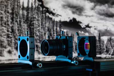
Senzor de imagine bazat pe fotodiodele organice pe siliciu, în aplicații tipice pentru camere. Context: Imagine NIR. (Imagine: Fraunhofer FEP, Fotograf: Jürgen Lösel)
Imaginile CMOS pe bază de siliciu convenționale sunt limitate la o regiune de lungime de undă restricționată din motive tehnologice fundamentale. Acestea sunt de obicei setate pe segmentul vizibil al spectrului. Dacă doriți să detectați lumina în infraroșu apropiat (NIR), cu toate acestea, soluții hibride, cum ar fi combinații de arsenid de iniu galiu (InGaAs) cu CMOS sunt, de obicei, recurs la.
Cu toate acestea, fabricarea acestor tipuri de soluții hibride este considerabil mai costisitoare și mai predispusă la defecte decât fabricarea utilizând procese standard CMOS. Aici fotodiodele organice oferă o alternativă. Straturile organice pot fi integrate pur și simplu la nivelul plachetelor și, prin urmare, sunt economice. În același timp, acestea pot avea, de asemenea, o sensibilitate ridicată în afara regiunii vizibile a lungimii de undă, în funcție de sistemul de materiale selectat

Posted: Sep 05, 2017

Organic photodiodes – more economical detectors for the NIR region

(Nanowerk News) The Fraunhofer Institute for Organic Electronics, Electron Beam and Plasma Technology FEP will be introducing a new generation of organic photodiodes on silicon substrates (OPD-on-silicon) during the SEMI European Imaging & Sensors Summit 2017, September 20-22 in Grenoble, France, at MINATEC, Booth 42.

Optical sensors are pervasive. Domestic life as well as the industrial environment are hard to imagine without them. For example, digital cameras using CMOS detectors have been indispensable vacation companions for many years, while in industry they serve as a simple and economical solution for automated image processing (such as in quality control applications, remote presence and position recognition and counting in conveyor systems, and object recognition in warehousing logistics). They can also be employed in medical engineering for diagnostic image processing. There are many future applications in the field of autonomous vehicles that are already foreseeable today.
Image sensor based on organic photodiodes on silicon in typical camera application
Image sensor based on organic photodiodes on silicon in typical camera application. Background: NIR image. (Image: Fraunhofer FEP, Photographer: Jürgen Lösel)
Conventional silicon-based CMOS imagers are limited to a restricted wavelength region for fundamental technological reasons. They are usually set to the visible segment of the spectrum. If you want to detect light in the near-infrared (NIR), however, hybrid solutions such as combinations of indium gallium arsenide (InGaAs) with CMOS are usually resorted to.
Nevertheless, the manufacture of these kinds of hybrid solutions is considerably more costly and more prone to defects than fabrication using standard CMOS processes. This is where organic photodiodes offer an alternative. The organic layers can be integrated simply at wafer level and are therefore economical. Simultaneously, they also may have high sensitivity outside the visible wavelength region, depending on the system of materials selected.
The Fraunhofer FEP has extensive experience in integrating organic layers on CMOS wafers. Diverse OLED microdisplays (high-resolution, low power, embedded image sensors, …) as well as sensors for fingerprint, flow, and photoelectric sensing applications have already been developed and fabricated.
“We will be debuting an organic photodiode array with SVGA resolution at SEMI European Imaging & Sensors Summit 2017. That means 800 × 600 pixels available for detection applications”, explains Philipp Wartenberg, head of the IC and System Design department at Fraunhofer FEP. “We have demonstrated that it is fundamentally feasible to fabricate a high-resolution organic photodiode matrix at this order of magnitude. It is sensitive at wavelengths up to 1,000 nanometers. We are able to develop customer- and application-specific organic photodiodes with optimized properties for the concrete application through appropriate adaption of material.”
The demonstrated image sensors were fabricated completely at wafer-level and therefore already under near-production conditions. With its extended region of sensitivity, the imager can be employed over the entire bandwidth of conventional applications in industry, automobiles, and medicine. They could be used for quality control of foodstuffs, as fingerprint sensors, and in biomedical tests, for example.
The scientists are now making the new technology available to industrial partners in order to jointly develop and produce optimized organic photodiodes and arrays as image sensors for their respective applications.
Source: Fraunhofer Institute for Organic Electronics, Electron Beam and Plasma Technology
Subscribe to a free copy of one of our daily
Nanowerk Newsletter Email Digests
with a compilation of all of the day’s news.

Read more: Organic photodiodes – more economical detectors for the NIR region

Nanoimateriale de carbon mai sigure, prin design (Nanoparticles limit damage in spinal cord injury)

Nanowerk News ) Nanomaterialele de carbon (CNM) sunt o clasă de nanomateriale fabricate care pot fi utilizate pentru multe aplicații de mediu, inclusiv tratarea apei și detectarea și remedierea contaminanților. În timp ce sunt apreciați pentru abilitatea lor de a detecta, îndepărta sau degrada contaminanții din mediul înconjurător, CNM-urile nu dispar doar după ce sunt folosite.
„Ca orice substanță chimică care persistă în mediul înconjurător, există îngrijorări cu privire la impactul asupra organismelor și sistemelor care rezultă din pericolul inerent al materialului, al produselor sale de degradare și al potențialului său de a se bioacumula – sau se acumulează în corpurile vieții,

Posted: Sep 05, 2017

Nanoparticles limit damage in spinal cord injury

(Nanowerk News) After a spinal cord injury, a significant amount of secondary nerve damage is caused by inflammation and internal scarring that inhibits the ability of the nervous system to repair itself.

A biodegradable nanoparticle injected after a spinal cord trauma prevented the inflammation and internal scarring that inhibits the repair process, reports a new Northwestern Medicine study.
As a result, mice with a spinal cord injury receiving the nanoparticle injection were able to walk better after the injury than those that didn’t receive it.
The treatment could potentially limit secondary damage to the spinal cord in humans after an injury, if administered a few hours after the accident in an emergency room or by paramedics in an ambulance.
“It’s not a cure. There is still the original damage, but we were able to prevent the secondary damage,” said co-senior author Dr. Jack Kessler, a professor of neurology at Northwestern University Feinberg School of Medicine and a Northwestern Medicine neurologist. “It’s an exciting potential treatment. We really believe this is something we’ll be able to take to the clinic.”
Further studies would need to confirm the safety of the injected nanoparticle, Kessler said, but he noted scientists haven’t seen any signs of toxicity so far.
The study was published in Neurobiology of Disease („Intravenous immune-modifying nanoparticles as a therapy for spinal cord injury in mice”).
The nanoparticles work by binding to the cells that cause the inflammation — inflammatory monocytes — and diverting them to the spleen. The particles are made of poly(lactic-co-glycolic) acid, a biocompatible substance already approved by the Food and Drug Administration (FDA) for use in re-absorbable sutures.
Developed in the lab of Northwestern scientist Stephen Miller, the particles also are FDA approved as an investigational drug for a new clinical trial in celiac disease.
“The study results suggest nanoparticle infusion could offer a novel and practical potential treatment for human spinal cord injury, a condition for which there are currently no effective treatments,” said Miller, the Judy Gugenheim Research Professor of Microbiology-Immunology at Feinberg.
After a spinal cord injury, blood cells that normally couldn’t enter the nervous system breech the protective blood brain barrier and flood the injury site. They release noxious chemicals, called inflammatory cytokines, which call in additional inflammatory blood cells. These cells further damage the central nervous system tissue by causing neuronal cell death and scar formation that blocks recovery from paralysis.
Two types of neurons die. One type — myelin — surrounds the nerve fibers and allows them to carry signals through the nervous system. If the myelin sheath is lost, the cells can no longer conduct signals. The other cells that die are axons, the long fibers extending from the neurons that carry signals from neuron to neuron.
“The new treatment is unusual because it is potentially immediately translatable to human beings,” Kessler said. “All we have to do is literally inject these beads into the blood stream. It doesn’t require surgery or any fancy intervention.”
The tiny beads also are very stable and can be kept in a syringe, Kessler noted. “An emergency medical technician at the site of an accident or somebody in an emergency room when someone is brought in can give this injection immediately,” he said.
Other researchers have tried techniques to block inflammatory monocytes from entering the nervous system after a spinal cord injury, but those methods blocked beneficial and harmful cells. The beneficial cells actually clean up the damage from the trauma and limit the scarring, so previous efforts resulted in only a modest improvement in scarring, cell death and repair.
The nanoparticle technology is being developed commercially by Cour Pharmaceuticals Development Co., which is working with Miller to bring this new approach to patients. Miller is a co-founder of Cour and a member of the scientific advisory board.
Miller also is a member of the Robert H. Lurie Comprehensive Cancer Center of Northwestern University.
Source: By Marla Paul, Northwestern University

Read more: Nanoparticles limit damage in spinal cord injury

Detectarea produselor alimentare contrafăcute(Detection of counterfeit food products )

Senzorul de pH fluorescent rasometric detectează modificările pH-ului în produsele lichide marcate atribuite contaminării bacteriene – o procedură comună în microbiologie

Detection

Prima analiză statică și dinamică a ceramicii tipărite sinterizate 3-D pentru aplicațiile de armură a corpului

Fabricarea tradițională a ceramicii utilizate pentru protecția împotriva impactului balistic este limitată de timpii lungi de plumb, de incapacitatea de a fabrica geometrii complexe și de componentele scumpe. Ceramica 3-D de tipărire oferă componente de inginerie la un timp de aproximativ 90% mai puțin decât fabricarea tradițională de ceramică. Schimbarea tipică poate fi zile, în loc de săptămâni, în funcție de complexitatea părții. Acest lucru permite un timp mai rapid de comercializare și permite mai multe iterații în timpul procesului de proiectare, rezultând un produs finit mai bun. În plus, piesele tipărite 3-D pot avea un grad mai mare de complexitate pentru reducerea greutății, economisind costul piesei, deoarece este necesar un material mai mic. Laboratorul de Cercetare al Armatei din S.U.A. (Adelphia, MD) a colaborat cu HotEnd Works LLC (Oberlin, Ohio) pentru a evalua fezabilitatea producerii armurii ceramice prin imprimare 3D. Acest raport examinează parametrii statici și cvasi-statici (inclusiv densitatea, duritatea și rezistența la fractură), performanța de penetrare semi-infinită și profilurile de fractură afectată a aluminei sinterizate tipărite 3-D în comparație cu performanța de bază a sinterizării tradiționale alumină

Fabricarea tradițională a ceramicii utilizate pentru protecția împotriva impactului balistic este limitată de timpii lungi de plumb, de incapacitatea de a fabrica geometrii complexe și de componentele scumpe. Ceramica 3-D de tipărire oferă componente de inginerie la un timp de aproximativ 90% mai puțin decât fabricarea tradițională de ceramică. Schimbarea tipică poate fi zile, în loc de săptămâni, în funcție de complexitatea părții. Acest lucru permite un timp mai rapid de comercializare și permite mai multe iterații în timpul procesului de proiectare, rezultând un produs finit mai bun. În plus, piesele tipărite 3-D pot avea un grad mai mare de complexitate pentru reducerea greutății, economisind costul piesei, deoarece este necesar un material mai mic. Laboratorul de Cercetare al Armatei din S.U.A. (Adelphia, MD) a colaborat cu HotEnd Works LLC (Oberlin, Ohio) pentru a evalua fezabilitatea producerii armurii ceramice prin imprimare 3D. Acest raport examinează parametrii statici și cvasi-statici (inclusiv densitatea, duritatea și rezistența la fractură), performanța de penetrare semi-infinită și profilurile de fractură afectată a aluminei sinterizate tipărite 3-D în comparație cu performanța de bază a sinterizării tradiționale alumină

Prima analiză statică și dinamică

ARL