
CERT: Aceste tehnologii emergente aduc noi riscuri(CERT :These emerging technologies bring new risks)
Tehnologiile emergente își găsesc drumul în viața de zi cu zi, pe măsură ce se maturizează și câștigă acceptarea
Tehnologiile emergente își găsesc drumul în viața de zi cu zi, pe măsură ce se maturizează și câștigă acceptarea
Filmele metalice cu o grosime de zeci de nanometri sau zeci de miliarde de metru sunt utilizate pe scară largă pentru a produce senzori compacți chimici și biologici, fotodetectoare, celule solare și componente pentru computere optice. Atunci când nanofilmele sunt mai subțiri decât 10 nanometri, ele devin nu doar conductive, ci și flexibile și transparente, care ar putea fi aplicabile într-o varietate de dispozitive moderne.Astfel de filme pot fi folosite în optică și optoelectronică pentru a dezvolta biosenzori compacți cu sensibilitate ridicată, celule solare, fotodetectoare în bandă largă și componente computerizate optoelectronice”. Filmele de aur de acest tip, cu o grosime de aproximativ 40 nanometri, sunt deja utilizate în proiectarea biosenzorilor.
| Posted: Oct 17, 2017 | |
Scientists revisit optical constants of ultrathin gold films(Nanowerk News) Researchers at Moscow Institute of Physics and Technology (MIPT) have conducted highly precise measurements of the optical constants of ultrathin gold films with thicknesses ranging from 20 to 200 billionths of a meter in the optical part of the electromagnetic spectrum. Thin gold films are key components of modern micro- and nanoscale optical and optoelectronic devices. The research findings will be in demand among researchers in the field. The paper was published in the journal Optics Express („Optical constants and structural properties of thin gold films”). |
|
| Metal films with a thickness of tens of nanometers, or tens of billionths of a meter, are widely used to produce compact chemical and biological sensors, photodetectors, solar cells, and components for optical computers. When nanofilms are made thinner than 10 nanometers, they become not just conductive but also flexible and transparent, which might be applicable in a variety of modern devices. | |
 |
|
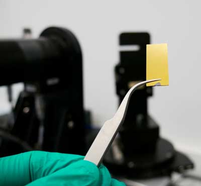
| Preparation of a thin gold film sample for spectroscopic ellipsometry measurements. (Image: MIPT) | |
| Gold, which is widely used in nanoscale device development, has proved to be the most suitable metal for the purpose. Such applications require gold in the form of very thin films or nanostructures. To develop and optimize devices, precise data on the properties of such films are necessary. But most of the data used by researchers at present are reported in papers published almost half a century ago. | |
| For instance, one of the most frequently cited articles on the optical constants of gold is „Optical constants of the noble metals” by P.B. Johnson and R.W. Christy, published as early as 1972. The Scopus citation database reveals that the reference constants for gold from this paper have been used in at least 10,000 other publications. To appreciate the significance of this work, it is important to keep in mind that in the 70s, research into the optical properties of thin metal films required a tremendous effort, because the challenging experiments had to be followed by complex calculations and computers were not yet widespread. | |
Thinner is better |
|
| State-of-the-art laboratory equipment and the nearly unlimited computing power available to modern researchers enable more detailed studies of thin metal films. However, it is known that the optical properties of such films – and therefore the efficiency of devices based on them – depend on factors such as film thickness, deposition rate, and the temperature of the substrate used for film deposition. | |
| Accordingly, the MIPT researchers adjusted the initial conditions, namely the deposition rate and the substrate temperature, so as to optimize the optical properties of the film. After that, they conducted the necessary measurements by means of spectroscopic ellipsometry, X-ray diffractometry, electron and atomic force microscopy. The data obtained allowed the MIPT team to study in detail how the properties of thin gold films are related to their structure and average grain size. | |
| The structure of a material affects its physical properties to a large extent, because it is at grain boundaries that conduction electrons are scattered, losing energy – the way a ball in a pinball machine loses its momentum as it runs into obstacles. As it turned out, both optical losses and direct current resistivity are substantially increased, as the thickness of the gold film is reduced to below 80 nanometers. | |
| The authors of the paper provide reference data on the optical constants of gold for a wide range of wavelengths, from 300 to 2,000 nanometers, for films that are 20 to 200 nanometers thick. These findings will be of use to researchers working on various nanophotonic devices and metamaterials. | |
State-of-the-art technology |
|
| To grow thin films, the researchers used a technique called electron beam evaporation, which involves the following steps:: A purified silicon substrate is introduced into a vacuum chamber. Opposite the substrate, a metal sample is positioned. The metal, in this case gold, is then subjected to a beam of electrons accelerated by an electric field. This rapidly heats up the gold causing it to melt and eventually transform into vapor. The evaporated gold atoms are then transported across a region of low pressure from their source and undergo condensation on the substrate to form the thin film. | |
| „Provided that you maintain a high vacuum, heat the metal appropriately, and otherwise follow the procedure, this technique yields films of arbitrary thickness, which is determined by the evaporation time. Moreover, the films are almost perfectly smooth, having a roughness of less than a nanometer,” comments Valentyn Volkov, who heads the Laboratory of Nanooptics and Plasmonics at MIPT. „Such films can be used in optics and optoelectronics to develop high-sensitivity compact biosensors, solar cells, broadband photodetectors, and optoelectronic computer components.” Gold films of this kind with a thickness of about 40 nanometers are already used in biosensor design. |
| Source: Moscow Institute of Physics and Technology |
au proiectat si testat o serie de matrice nanoantenna plasmonica care ar putea duce la dezvoltarea unei noi generatii de senzori de fluorescenta ultrasensibili si cu costuri reduse care ar putea să fie utilizat pentru a monitoriza calitatea apei.care dezvoltă senzori de fluorescență cuantificați, care vor ajuta la identificarea bacteriilor în câteva minute, nu în câteva zile.
| Posted: Oct 16, 2017 | |
Nanoantenna arrays power a new generation of fluorescence-based sensors(Nanowerk News) Researchers from the Universities of Bristol and Bedfordshire, in collaboration with multinational company ABB, have designed and tested a series of plasmonic nanoantenna arrays that could lead to the development of a new generation of ultrasensitive and low-cost fluorescence sensors that could be used to monitor water quality. |
|
| The arrays, designed and tested by Dr Neciah Dorh during his PhD at the University of Bristol, are made from aluminium nanorods fabricated using electron beam lithography by commercial partner Kelvin Nanotechnologies. The nanorods, 50nm wide and 158nm long, are designed to resonantly enhance fluorescence emission from a range of contaminants in water such as diesel or tryptophan. | |
 |
|
| SEM images of nanoantenna array and in the inset a magnified view of the array elements. (Image: University of Bristol) | |
| The work, published in Applied Optics („Nanoantenna arrays combining enhancement and beam control for fluorescence-based sensing applications”), shows a six-fold increase in measured fluorescence emission from a dye. The research also shows that by correctly designing the array element spacing, strongly directional fluorescent emission can be obtained which would allow for highly integrated multi-wavelength sensors to be designed. | |
| The work was carried out in Professor Martin Cryan’s research group, which is part of the Photonics Research group in the Department of Electrical and Electronic Engineering. | |
| The project was a collaboration with Dr Andrei Sarua from the School of Physics at Bristol and Dr Tahmina Ajmal from the University of Bedfordshire, who had previously worked on the Aquatest project at Bristol. | |
| Together they developed a prototype low-cost, LED based sensor system, which they plan to develop further into a hand-held field deployable system for performing water quality monitoring. | |
| Martin Cryan, Professor of Applied Electromagnetics and Photonics in the Department of Electrical and Electronic Engineering at the University of Bristol and co-author on the paper, said: „The nanoantenna arrays, which can be fabricated by lower cost production techniques such as nanoimprint lithography, can bring significant sensitivity enhancement so that laboratory quality measurements could be carried out in the field. This would allow for deployment of remote wireless sensor networks for early warning of pollution or continuous monitoring of water quality in sensitive environments.” | |
| Dr Dorh, now a Fellow within Bristol’s QTEC programme, has co-founded a start-up, FluoretiQ, developing quantum enhanced fluorescence sensors which will help identify bacteria within minutes rather than days. | |
| Professor Cryan’s group is developing systems that could combine the power of nanoantennas with quantum enhanced sensors to produce yet further sensitivity enhancements. |
| Source: University of Bristol |
Simulările sugerează că laserul SPP ar putea deveni un detector și mai sensibil pentru materialele biologice, chimice și de mediu decât utilizarea doar a cavității rezonante. Designul laserului permite, de asemenea, integrarea ușoară într-un circuit fotonic și poate permite, de asemenea, noi studii ale plasmonicii cuantice, interacțiunea nanometrică a materiei cu proprietățile cuantice ale luminii.
| Posted: Oct 13, 2017 | |
Plasmons in an open box create miniature laser(Nanowerk News) Scientists at the National Institute of Standards and Technology (NIST) have developed the first miniature laser in which the light is guided along the floor of an open metallic trench. The laser could act as a nanoscale device to sense minute amounts of pollutants and other chemicals in the environment, or detect the surface binding of biomolecules for medical diagnostics. |
|
| Wenqi Zhu of NIST and the University of Maryland, along with NIST physicists Henri Lezec and Amit Agrawal, described their work (link is external) in a recent edition of Science Advances(„Surface-Plasmon-Polariton Laser based on a Metallic Trench Fabry-Perot Resonator”). The work was performed in collaboration with Nanjing University in China and the University of Michigan. | |
 |
|
| Illustration depicts cavity and sidewalls, made of silver, that form the miniature laser fabricated by scientists working at NIST. The cavity’s ultrathin coating (flat red layer) is the amplifying layer used to induce SPP lasing under illumination from above (blue-green light beam); a small amount of the red laser light leaks through a nanoscale notch positioned just below the cavity’s floor enabling researchers to monitor small wavelength shifts induced by the presence of the molecules on the cavity floor. (Image: NIST) | |
| The development of the new laser relies on the interaction between photons—particles of light—and the sea of electrons that floats along the surface of a metal. Interactions between the photons and ripples in the electron sea yield a special type of light wave, dubbed a surface plasmon polariton (SPP), which is tightly confined to travel only along the metal’s surface. This confinement makes the SPPs highly sensitive to anything lying on the metal surface. | |
| As a first step toward building the miniature laser, the team fashioned out of silver a small trench-shaped open cavity in which SPPs can resonate. The cavity is a flat surface flanked by tiny, mirror-like sidewalls that reflect the surface waves back and forth. | |
| Through careful fabrication, the resonant cavity possessed two key properties: all of its interior surfaces were smooth on an atomic scale, varying in thickness by no more than a few nanometers, and its sidewalls were perpendicular with respect to the flat cavity floor. The design, made possible by molding silver using a precisely patterned silicon template, enabled the SPPs to bounce back and forth across the cavity hundreds of times without losing significant energy, like a guitar string sustaining a pure note for a long time. That property, known as high quality factor, or high Q, is essential for constructing a laser. The Q measured by the team is the highest to date for any visible-light resonator using only SPPs. | |
| The high Q also enabled the cavity to act as an extremely selective filter for SPPs—only those with wavelengths that fell within a narrow band could resonate in the cavity. The narrow range is important because it enables the resonant cavity (even before it became part of a laser) to become a highly sensitive detector of tiny changes in its environment—the presence of particulate matter or the addition of a thin film to the cavity’s floor. Such changes shift the center of the band of wavelengths that will resonate in the cavity. | |
| “By achieving a narrow resonance, the shift in wavelength is clear, and the open cavity can act as an exquisitely sensitive detector,” said Lezec. | |
| After demonstrating that the cavity could be used as a sensor, the team then worked to turn their design into a laser. They did so by adding an ultrathin coating to the cavity that amplified the intensity of the SPP traveling through the structure. This is the first nanoscale laser ever constructed by manipulating an SPP traveling on a single flat metal surface, Lezec noted. | |
| Simulations suggest the SPP laser could become an even more sensitive detector for biological, chemical and environmental materials than using just the resonant cavity. The design of the laser also enables it to be easily integrated into a photonic circuit and may also enable new studies of quantum plasmonics, the nanoscale interaction of matter with the quantum properties of light. |
| Source: NIST |
Armura lichidă dezvoltată la Universitatea din Delaware poate fi vopsită pe țesături, ceea ce face ca materialul textil să fie extrem de dificil de pătruns
au folosit o structură metalică organică bazată pe cobalt, care a imitat conductivitatea unui metal și a unui semiconductor la diferite temperaturi. Cadrul metalic-organic creat de oamenii de știință a demonstrat cea mai mare conductivitate la temperaturi foarte scăzute și foarte ridicate.
| Posted: Oct 12, 2017 | |
A metal-organic framework solution for storing renewable energy(Nanowerk News) Scientists have long searched for the next generation of materials that can catalyze a revolution in renewable energy harvesting and storage. |
|
| One candidate appears to be metal-organic frameworks. Scientists have used these very small, flexible, ultra-thin, super-porous crystalline structures to do everything from capturing and converting carbon into fuels to storing hydrogen and other gases. Their biggest drawback has been their lack of conductivity. | |
| Now, according to USC scientists, it turns out that metal-organic frameworks can conduct electricity in the same way metals do. | |
 |
|
| The cobalt-based metal-organic framework used by the USC scientists, with purple representing cobalt, yellow representing sulfur and gray representing carbon. (Image: Smaranda Marinescu) | |
| This opens the door for metal organic-frameworks to one day efficiently store renewable energy at a very large, almost unthinkable scale. | |
| „For the first time ever, we have demonstrated a metal-organic framework that exhibits conductivity like that of a metal. The natural porosity of the metal-organic framework makes it ideal for reducing the mass of material, allowing for lighter, more compact devices” said Brent Melot, assistant professor of chemistry at the USC Dornsife College of Letters, Arts & Sciences. | |
| „Metallic conductivity in tandem with other catalytic properties would add to its potential for renewable energy production and storage” said Smaranda Marinescu, assistant professor of chemistry at the USC Dornsife College. | |
| Their findings were published in the Journal of the American Chemical Society („Metallic Conductivity in a Two-Dimensional Cobalt Dithiolene Metal–Organic Framework”). | |
An emerging catalyst for long-term renewable energy storage |
|
| Metal-organic frameworks are so porous that they are well-suited for absorbing and storing gases like hydrogen and carbon dioxide. Their storage is highly concentrated: 1 gram of surface area provides the equivalent of thousands of square feet in storage. | |
| Solar has not yet been maximized as an energy source. The earth receives more energy from one hour of sunlight than is consumed in one year by the entire planet, but there is currently no way to use this energy because there is no way to conserve all of it. This intermittency is intrinsic to nearly all renewable power sources, making it impossible to harvest and store energy unless, say, the sun is shining or the wind is blowing. | |
| If scientists and industries could one day regularly reproduce the capability demonstrated by Marinescu, it would go a long way to reducing intermittency, allowing us to finally make solar energy an enduring and more permanent resource. | |
Metal or semiconductor: why not both? |
|
| Metal-organic frameworks are two-dimensional structures that contain cobalt, sulfur, and carbon atoms. In many ways, they very broadly resemble something like graphene, which is also a very thin layer of two-dimensional, transparent material. | |
| As temperature goes down, metals become more conductive. Conversely, as the temperature goes up, it is semiconductors that become more conductive. | |
| In the experiments run by Marinescu’s group, they used a cobalt-based metal-organic framework that mimicked the conductivity of both a metal and semiconductor at different temperatures. The metal-organic framework designed by the scientists demonstrated its greatest conductivity at both very low and very high temperatures. |
| Source: University of Southern California |
Fluidele de îngroșare prin forfecare permează țesăturile și straturile de material cu o tehnologie remarcabilă, care devine efectiv mai puternică atunci când este lovită cu o forță crescândă, ceea ce face ca materialul să fie puternic pătruns și rezistent la balistice. La fel de uimitor, materialul adăugat nanocompozit, denumit uneori „armură lichidă”, dar marcat ca STF-Armor, adaugă o greutate redusă materialului și nu reduce flexibilitatea acestuia – două caracteristici critice pentru un costum de spațiu.aplicate habitatelor spațioase gonflabile, precum și echipamente de protecție, echipamente de luptă împotriva incendiilor și de aplicare a legii, mănuși industriale și costume de hazmat
| Posted: Oct 12, 2017 | |
‘Liquid armor’ toughens spacesuits(Nanowerk News) Astronauts are a smart, courageous and resilient lot, no doubt about that. But when they go out for a walk in space – in environments none of us could survive on our own – they need a lot of protection. |
|
| There are plenty of perilous possibilities. One of the most serious threats is the stuff flying around in space – sharp stuff, dusty stuff, fast-moving stuff. | |
| Puncture an astronaut’s space suit – whether by projectile, the sharp edge of a tool or falling onto a rock – and you could let in a world of trouble. | |
 |
|
| ‘Liquid armor” developed at the University of Delaware can be painted on fabric, making the textile extremely difficult to puncture. (Image: University of Delaware) | |
| NASA sees great promise in a new protective textile – the shear thickening fluid technology co-developed at the University of Delaware by Norman Wagner, Unidel Robert L. Pigford Chair in Chemical and Biomolecular Engineering, and STF Technologies, the company he co-founded with UD alum Richard Dombrowski. | |
| Shear thickening fluids permeate fabrics and layers of material with a remarkable technology that actually gets stronger when it is struck with increasing force, making the material highly puncture and ballistic-resistant. Just as amazing, the added nanocomposite material, sometimes called „liquid armor,” but trademarked as STF-Armor, adds little weight to the fabric and does not reduce its flexibility – two critical features for a space suit. | |
| After proving its mettle with support from a NASA Small Business Innovation Research Phase 1 contract, STF Technologies has won a $750,000 Small Business Technology Transfer Research Phase II grant to produce a prototype that will shield astronauts whether they are in low-earth orbit – as they are at the International Space Station – on the moon or stepping onto Mars. | |
| That project has many benefits for ongoing work, too, including development of the Z2 spacesuit for NASA’s Journey to Mars mission. UD’s Center for Composite Materials has been integral to that effort, providing innovative components for the overall design created by ILC Dover. | |
| „It’s the same overall suit, but different aspects of it,” said Wagner, who has worked extensively with CCM. „They’re separate projects but both are related to making the suit better.” | |
| Wagner, a fellow in the National Academy of Inventors, was co-author of three presentations at the recent International Space Station Research & Development Conference in Washington D.C., including discussion of experiments his lab will do on the ISS and ways STF-Armor could be applied to inflatable space habitats as well as protective equipment, firefighting and law enforcement gear, industrial gloves and hazmat suits. With UD Prof. Christopher Kloxin (chemical & biomolecular engineering, materials science & engineering) and UD alum Melissa Gordon (now on the faculty at Lafayette College), Wagner explained recent advances with „self-healing” materials. | |
| Near-future plans include launching STF’s materials on a November trip to the ISS, where it will be placed outside the space station for a year and then analyzed to see how it fares in that environment. | |
| Undergraduates will have opportunity to be part of STF Technologies’ work through the Office of Economic Innovation and Partnership’s Spin-In Program, a popular and successful collaboration between UD students and business entrepreneurs who need their engineering, business or policy savvy. | |
| „NASA funding for small-business development has an expectation that space technology will have earth-based benefits, and they generally do,” Wagner said. | |
| The project brings many layers of innovation together – linking NASA’s missions with the research and innovation produced by Wagner and other researchers and giving students and business owners opportunity to contribute to significant projects, gaining invaluable experience. | |
| „Human exploration of space inspires people to do great things,” Wagner said. „And it attracts a lot of interesting, good people.” |
| Source: University of Delaware |
Ideea dopajului de electroni pentru a modifica strucCercetatorii au folosit ditelluri de molibden (MoTe 2 ), un semiconductor tipic 2-D, si au acoperit-o cu un lichid ionic (DEME-TFSI), care are o capacitate ultra-mare sau capacitatea de a stoca incarcatura electrica. Stratul de lichid ionic a permis cercetătorilor să injecteze semiconductorul cu electroni la o densitate de o sută de bilioane la un cvadrilioane pe centimetru pătrat. Este o densitate de electroni care este una-două ordine mai mare decât cea care ar putea fi obținută în materialele 3-D în vrac, au spus cercetătorii.tura atomică a materialului este unică pentru materialele 2-D, care sunt mult mai ușor de reglabil electric în comparație cu materialele în vrac 3-D”,
| Postat: 11 octombrie 2017 | |
Injectarea electronilor distruge structura 2D în noul model atomic( Nanowerk News ) Aceeași încărcătură electrostatică care poate face ca părul să stea pe capăt și să atragă baloane la îmbrăcăminte ar putea fi o modalitate eficientă de a conduce vehicule subțiri subțiri cu memorie electronică ale viitorului, potrivit unui nou studiu condus de cercetători de la Departamentul Energiei Lawrence Laboratorul Național Berkeley (Laboratorul Berkeley). |
|
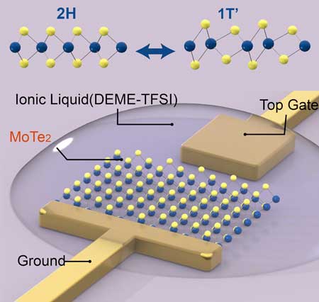
| Intr-un studiu publicat astazi in revista Nature ( „Transformarea fazei structurale in monostratul MoTe 2 condus de dopajul electrostatic” ), oamenii de stiinta au gasit o modalitate de a schimba in mod reversibil structura atomica a unui material 2-D prin injectare sau „doping” cu electroni.Procesul utilizează mult mai puțină energie decât metodele curente pentru a schimba configurația structurii unui material. | |
 |
|
| Schema prezintă configurația pentru tranziția fazei structurale pe un monostrat de molibden ditelluride (MoTe 2 , prezentat ca sfere galbene și albastre), care este ancorat de un electrod metalic (poarta de sus și sol). Lichidul ionic care acoperă monostratul și electrozii permite o densitate mare de electroni să populeze monostratul, ceea ce duce la modificări ale laturii structurale de la un model hexagonal (2H) la un monoclinic (1T ‘). (Credit: Ying Wang / Berkeley Lab) | |
| „Arătăm pentru prima dată că este posibil să se injecteze electroni pentru a conduce schimbări de fază structurală în materiale”, a declarat cercetătorul principal al studiului, Xiang Zhang, om de știință de la Facultatea de Materiale Berkeley Lab și profesor la UC Berkeley. „Prin adăugarea de electroni într-un material, energia totală urcă și va sfârși balanța, rezultând structura atomică rearanjând un nou model care este mai stabil. O astfel de tranziție a fazei structurale determinată de dopajul electronic la limita 2-D nu este importantă numai în fizica fundamentală; de asemenea, deschide ușa pentru noua memorie electronică și comutarea la putere redusă în următoarea generație de dispozitive ultra-subțiri. „ | |
| Comutarea configurației structurale a unui material de la o fază la alta este caracteristica fundamentală, binară care stă la baza circuitelor digitale actuale. Componentele electronice capabile de această tranziție de fază s-au diminuat până la dimensiuni subțiri de hârtie, dar ele sunt încă considerate a fi vrac, straturi 3D de către oamenii de știință. Prin comparație, materialele monostrat 2-D sunt compuse dintr-un singur strat de atomi sau molecule a căror grosime este de 100.000 de ori mai mică decât părul uman. | |
| „Ideea dopajului de electroni pentru a modifica structura atomică a materialului este unică pentru materialele 2-D, care sunt mult mai ușor de reglabil electric în comparație cu materialele în vrac 3-D”, a declarat co-lead autorul Jun Xiao, student în laboratorul Zhang . | |
| Abordarea clasică de a conduce tranziția structurală a materialelor implică încălzirea la peste 500 de grade Celsius. Astfel de metode sunt intensive din punct de vedere energetic și nu sunt fezabile pentru aplicații practice. În plus, căldura în exces poate reduce semnificativ durata de viață a componentelor în circuitele integrate. | |
| Un număr de grupuri de cercetare au investigat, de asemenea, utilizarea substanțelor chimice pentru a modifica configurația atomilor din materialele semiconductoare, dar acest proces este încă dificil de controlat și nu a fost adoptat pe scară largă de către industrie. | |
| „Aici folosim dopajul electrostatic pentru a controla configurația atomică a unui material bidimensional”, a declarat co-autorul studiului Ying Wang, un alt student absolvent în laboratorul lui Zhang. „În comparație cu utilizarea substanțelor chimice, metoda noastră este reversibilă și fără impurități. Are un potențial mai mare de integrare în fabricarea de telefoane mobile, computere și alte dispozitive electronice”. | |
| Cercetatorii au folosit ditelluri de molibden (MoTe 2 ), un semiconductor tipic 2-D, si au acoperit-o cu un lichid ionic (DEME-TFSI), care are o capacitate ultra-mare sau capacitatea de a stoca incarcatura electrica. Stratul de lichid ionic a permis cercetătorilor să injecteze semiconductorul cu electroni la o densitate de o sută de bilioane la un cvadrilioane pe centimetru pătrat. Este o densitate de electroni care este una-două ordine mai mare decât cea care ar putea fi obținută în materialele 3-D în vrac, au spus cercetătorii. | |
| Prin analiza spectroscopică, cercetătorii au stabilit că injectarea de electroni a schimbat dispunerea atomilor de ditelluri de molibden de la o formă hexagonală la una care este monoclinică, care are mai mult o formă cuboidă înclinată. Odată ce electronii au fost retrași, structura cristalină a revenit la modelul său hexagonal original, arătând că tranziția de fază este reversibilă. Mai mult decât atât, aceste două tipuri de aranjamente atomice au simetrii foarte diferite, oferind un contrast mare pentru aplicațiile componentelor optice. | |
| „Un astfel de dispozitiv subțire atomică ar putea avea funcții duale, care ar servi simultan ca tranzistori optici sau electrici și, prin urmare, vor lărgi funcționalitățile electronicii folosite în viața noastră de zi cu zi”, a spus Wang. |
| Sursă: Laboratorul Berkeley |
Există în prezent destul de multe obstacole atunci când vine vorba de construirea acestor super-avioane,
cercetatorii au demonstrat ca generatoarele termoelectrice care pot recupera energia din caldura corporala pot fi folosite pentru a alimenta biosenzori simpli pentru masurarea frecventei cardiace, a respiratiei sau a altor factori.”Comunitatea electronică a făcut progrese extraordinare în înțelegerea proprietăților electronice și optice ale materialelor pe bază de polimeri. Construim aceste cunoștințe pentru a înțelege transportul termic și termoelectric în aceste polimeri pentru a permite noi funcționalități ale dispozitivului. ”
Printre celelalte perspective ale materialelor dezvoltate se numără dispozitive de răcire localizate care inversează procesul, folosind electricitatea pentru a transfera energia termică dintr-o parte a unui dispozitiv în altul. Răcirea doar a unor părți ale corpului ar putea oferi percepția confortului fără costul aerului condiționat mare.
| Posted: Oct 09, 2017 | |
Novel circuit design boosts wearable thermoelectric generators(Nanowerk News) Using flexible conducting polymers and novel circuitry patterns printed on paper, researchers have demonstrated proof-of-concept wearable thermoelectric generators that can harvest energy from body heat to power simple biosensors for measuring heart rate, respiration or other factors. |
|
| Because of their symmetrical fractal wiring patterns, the devices can be cut to the size needed to provide the voltage and power requirements for specific applications. The modular generators could be inkjet printed on flexible substrates, including fabric, and manufactured using inexpensive roll-to-roll techniques. | |
| “The attraction of thermoelectric generators is that there is heat all around us,” said Akanksha Menon, a Ph.D. student in the Woodruff School of Mechanical Engineering at the Georgia Institute of Technology. “If we can harness a little bit of that heat and turn it into electricity inexpensively, there is great value. We are working on how to produce electricity with heat from the body.” | |
| The research was reported in the Journal of Applied Physics („Interconnect patterns for printed organic thermoelectric devices with large fill factors”) | |
 |
|
| Electrical conductivity is measured for a thermoelectric polymer film in the laboratory of Shannon Yee at the Georgia Institute of Technology. (Image: Georgia Tech) | |
| Thermoelectric generators, which convert thermal energy directly into electricity, have been available for decades, but standard designs use inflexible inorganic materials that are too toxic for use in wearable devices. Power output depends on the temperature differential that can be created between two sides of the generators, which makes depending on body heat challenging. Getting enough thermal energy from a small contact area on the skin increases the challenge, and internal resistance in the device ultimately limits the power output. | |
| To overcome that, Menon and collaborators in the laboratory of Assistant Professor Shannon Yee designed a device with thousands of dots composed of alternating p-type and n-type polymers in a closely-packed layout. Their pattern converts more heat per unit area due to large packing densities enabled by inkjet printers. By placing the polymer dots closer together, the interconnect length decreases, which in turn lowers the total resistance and results in a higher power output from the device. | |
| “Instead of connecting the polymer dots with a traditional serpentine wiring pattern, we are using wiring patterns based on space filling curves, such as the Hilbert pattern – a continuous space-filling curve,” said Kiarash Gordiz, a co-author who worked on the project while he was a Ph.D. student at Georgia Tech. “The advantage here is that Hilbert patterns allow for surface conformation and self-localization, which provides a more uniform temperature across the device.” | |
| The new circuit design also has another benefit: its fractally symmetric design allows the modules to be cut along boundaries between symmetric areas to provide exactly the voltage and power needed for a specific application. That eliminates the need for power converters that add complexity and take power away from the system. | |
| “This is valuable in the context of wearables, where you want as few components as possible,” said Menon. “We think this could be a really interesting way to expand the use of thermoelectrics for wearable devices.” | |
| So far, the devices have been printed on ordinary paper, but the researchers have begun exploring the use of fabrics. Both paper and fabric are flexible, but the fabric could be easily integrated into clothing. | |
| “We want to integrate our device into the commercial textiles that people wear every day,” said Menon. “People would feel comfortable wearing these fabrics, but they would be able to power something with just the heat from their bodies.” | |
| With the novel design, the researchers expect to get enough electricity to power small sensors, in the range of microwatts to milliwatts. That would be enough for simple heart rate sensors, but not more complex devices like fitness trackers or smartphones. The generators might also be useful to supplement batteries, allowing devices to operate for longer periods of time. | |
| Among the challenges ahead are protecting the generators from moisture and determining just how close they should be to the skin to transfer thermal energy – while remaining comfortable for wearers. | |
| The researchers use commercially-available p-type materials, and are working with chemists at Georgia Tech to develop better n-type polymers for future generations of devices that can operate with small temperature differentials at room temperatures. Body heat produces differentials as small as five degrees, compared to a hundred degrees for generators used as part of piping and steam lines. | |
| “One future benefit of this class of polymer material is the potential for a low-cost and abundant thermoelectric material that would have an inherently low thermal conductivity,” said Yee, who directs the lab as part of the Woodruff School of Mechanical Engineering. “The organic electronics community has made tremendous advances in understanding electronic and optical properties of polymer-based materials. We are building upon that knowledge to understand thermal and thermoelectric transport in these polymers to enable new device functionality.” | |
| Among the other prospects for the materials being developed are localized cooling devices that reverse the process, using electricity to move thermal energy from one side of a device to another. Cooling just parts of the body could provide the perception of comfort without the cost of large-space air conditioning, Yee said. |
| Source: Georgia Institute of Technology |
tencuială la răni interne.
Acum există un adeziv de țesut inovator, al cărui scop este de a ajuta la închiderea optimă a rănilor în zonele în care acestea sunt dificil de localizat sau accesate și pentru a evita hemoragii difuze și care pun viața în pericol. Ideea unui adeziv de țesut nu este nouă: clemele convenționale constau în principal din fibrină, o proteină produsă de organism, care joacă un rol esențial în coagularea sângelui. Fibrina nu este numai foarte scumpă, dar poate declanșa și răspunsuri imune, care de multe ori duc la complicații grave.
| Posted: Oct 09, 2017 | |
Nanoparticles that stick wounds together(Nanowerk News) In spite of medical advances, wound-related complications arising after operations can still be life-threatening. In order to avoid these complications in the future, a new nanoparticle-based tissue glue has been developed by researchers at Empa. |
|
| There are internal and external areas of the body where it is difficult to apply stitches. Although medical science has made considerable progress in recent decades, complications still arise, especially after operations. In some cases, these are fatal. Particularly with internal wounds, there is a risk of haemorrhage, which is difficult to treat because it is not easy to stitch or apply a plaster to internal wounds. | |
| Now there is an innovative tissue glue, the purpose of which is to help to close wounds optimally in areas where they are difficult to locate or access, and to avoid diffuse and often life-threatening haemorrhages. The idea of a tissue glue is not new: conventional glues consist primarily of fibrin, a protein produced by the body which plays a key role in clotting the blood. Fibrin is not only very expensive, but can also trigger immune responses, which frequently result in serious complications. | |
 |
|
| Pig intestines were used for testing the new nanoparticle-based tissue glue. (Image: Empa) | |
An adhesive that also heals |
|
| As described recently in the specialist literature, it has now been discovered that nanoparticles have an adhesive property, known as „nano-bridging”. In the study in question, researchers used silica (silicon dioxide) and iron oxide nanoparticles to stick pieces of tissue together. Under Inge Herrmann’s leadership, researchers at Empa used this innovative principle to develop a tissue glue to be used in the future for various operations and complaints. They created nanoparticles from various material combinations, with a view to making the glue bioactive. | |
| And they succeeded. A combination of glue and bioglass makes the blood clot more quickly at the location of the wound. Depending on the combination of the elements silicon, calcium, sodium and phosphorus, bioglass has various different properties. If the ideal combination is achieved, this will open up completely new treatment possibilities. Depending on the formula, for example, bioglass may form effective bonds with bones or soft tissue. The researchers also ensured that none of the materials used is harmful to health. | |
First study of potential surgical use is published |
|
| Doctors helped the Empa research team to develop the tissue glue. For example, they expressed their wish to use the glue for intestinal tears. If the intestinal wall is damaged, tissue-damaging substances may leak out – so a glue of this kind would be ideal. | |
| In their study (Nanoscale, „Developing a tissue glue by engineering the adhesive and hemostatic properties of metal oxide nanoparticles”), the Empa researchers aimed to fulfil the doctors’ wish. Martin Matter, a doctoral candidate in Herrmann’s team and lead author of the study, used pig intestines to test the new glue. He investigated its capacity to glue the intestines together in the Empa textile laboratory in St. Gallen, by using a machine that usually tests the tear strength of materials. The first findings were extremely promising. So promising, in fact, that this line of research is still being pursued. Herrmann is convinced that there are further exciting possibilities for the glue if it is given additional properties. |
| Source: By Cornelia Zogg,Empa |