
Eugenică invizibilă(Invisible Eugenics)
Modul în care sistemul medical și școlile publice ucid copiii dumneavoastră
Modul în care sistemul medical și școlile publice ucid copiii dumneavoastră
Elite financiare;Războiul Împotriva Populației civile
LCSS-urile pot fi setate de obicei în 20-25 de minute;Se umplu umbrele modelate care distrug contururile caracteristice ale unui obiect
au creat noi superconductori din straturi de sulfură de bismut (BiS2) și o fluorfluorură de aliaj de pământuri rare de entropie, conținând cinci elemente diferite de pământuri rare în același sit cristalografic. Noul material păstrează proprietățile supraconductoare într-o gamă mai largă de parametri de zăcământ decât materiale fără stări de aliaj cu entropie ridicată.
| Posted: May 04, 2018 | |
Making new layered superconductors using high entropy alloys(Nanowerk News) Researchers from Tokyo Metropolitan University have created new superconductors made of layers of bismuth sulfide (BiS2) and a high entropy rare earth alloy oxyfluoride, containing five different rare earth (RE) elements at the same crystallographic site. The new material retains superconducting properties over a wider range of lattice parameters than materials without high-entropy-alloy states. |
|
| Their work promises an exciting new strategy for designing new layered superconductors, a potentially key development in the search for high-temperature superconductors (Applied Physics Express, „Superconductivity in REO0.5F0.5BiS2 with high-entropy-alloy-type blocking layers”). | |
 |
|
| This is a schematic image of the crystal structure of high-entropy-alloy-type REO0.5F0.5BiS2. (Image: Yoshikazu Mizuguchi) | |
| Superconductors are key to a range of exciting potential applications. For example, zero resistivity promises loss-free power transmission and powerful electromagnets. The challenge has been to discover a material that retains this property at higher temperatures, closer to ambient temperatures. Despite focused work and a number of breakthroughs in recent years, the hunt is still on for effective strategies to create new superconducting materials. | |
| One strategy is the use of layered materials with a molecular structure consisting of alternating superconducting layers and „blocking layers” acting as insulating spacers. A team led by Associate Professor Yoshikazu Mizuguchi from the Department of Physics, Tokyo Metropolitan University, has uncovered an important aspect of designing the insulating layer. They were able to combine five different rare earth (RE) elements, lanthanum, cerium, praseodymium, neodymium, and samarium, and create a „high entropy alloy” in the blocking layer. | |
| High entropy alloys have attracted considerable attention in recent years for their toughness, resistance to fatigue and ductility, amongst many other notable physical properties. | |
| The team’s new materials, with different proportions of REs (10-30%), exhibited enhanced superconducting properties; in particular, materials with the same period in their molecular structure exhibited a superconducting transition at higher temperatures when the blocking layer contained a high entropy alloy. They believe that the high entropy alloy helps to stabilize the crystal structure of the superconducting layer. | |
| The work’s impact is not limited to the new materials they present. Given the existence of a large number of superconducting layers which are compatible with RE oxides, this innovation opens the way for a broad new strategy for engineering new, revolutionary superconducting materials. |
| Source: Tokyo Metropolitan University |
Membranele de polimer, care acționează ca un filtru pentru desalinizarea și îndepărtarea selectivă a contaminanților din diferite surse de apă, au ajutat la tratarea apei, însă selectivitatea lor rămâne o provocare semnificativă în ceea ce privește filtrarea proprietăților chimice – un potențial risc pentru mediu și sănătatea umană.
| Posted: May 04, 2018 | |
Engineered polymer membranes could be new option for water treatment(Nanowerk News) The world’s freshwater resources are in short supply. According to the United Nations, water scarcity affects an estimated 1.9 billion people and 2.1 billion people live with drinking water services that are not safely managed. The critical point of water scarcity has led scientists to look for new and efficient ways to make the most of nontraditional sources, including sea water, brackish water and wastewater. |
|
| Polymer membranes, which act as a filter to desalinate and selectively remove contaminants from various water sources, have aided water treatment, but their selectivity remains a significant challenge when it comes to filtering chemical properties — a potential risk to the environment and human health. | |
| Chemical and biomolecular engineers at the University of Notre Dame and Purdue University studied self-assembled block polymer membranes, which allow for both customizable and uniform pore sizes, as a platform for water treatment systems. The study, published in Clean Water („Fit-for-purpose block polymer membranes molecularly engineered for water treatment”), determined the platform has the potential to advance water treatment technologies. | |
| “Most state-of-the-art membranes for water treatment are designed to let water pass through while filtering contaminants,” said William Phillip, associate professor in the Department of Chemical and Biomolecular Engineering at Notre Dame. “This approach limits the ability to remove or recover dissolved species based on their chemical identity. The exciting thing about self-assembled block polymer membranes is that you can engineer the nanostructure and pore wall chemistry of the membrane through the design of the block polymer molecules. This capability has the potential to open up a variety of new separation mechanisms that can isolate species based on chemical identity, which in turn could help to enable decentralized reuse of wastewater.” | |
| Phillip and the research team focused on block polymer membranes because of their well-defined nanostructures and functionality. They were able to molecularly engineer the chemical properties of the polymer to create large areas of high-performance membrane, reduce pore size and design multifunctional pore wall chemistries for solute-specific separation. The membranes could essentially be customized depending on the water source and treatment needed. | |
| Membranes that are more selective and more resilient to certain exposures such as chlorine or boric acid and less prone to collecting unwanted properties — or fouling — than current state-of-the-art options could improve treatment in a number of ways. They could reduce the number of filtration passes required for irrigation, control concentrations of chlorine into the system to help forestall effects of biofouling and reduce chemical demands for membrane cleaning — reducing operating costs and environmental impact. | |
| The global applications are significant when considering those populations without suitable drinking water and limited resources. | |
| Transitioning the technology from the laboratory setting to practice presents its own set of challenges that will need to be addressed in the coming years. However, the researchers are hopeful the transition can be made since several of the techniques used to generate self-assembled block polymers are consistent with current membrane fabrication practices. |
| Source: By Jessica Sieff, University of Notre Dame |
Un material poros cu buzunare personalizate în structura sa este un material promițător pentru detectarea gazelor nocive. O peliculă subțire de material, acoperit pe un electrod, format un senzor electronic care ar putea detecta urme de dioxid de sulf gazos ( Journal of Materials Chemistry , „SO foarte sensibil și selectiv 2 senzor MF: integrarea MFM-300 MOF ca sensibil strat pe un electrod capsiv interdigitat ” ). Senzorul este un pas important către dispozitivele din lumea reală care pot străpunge gazele periculoase în aerul real.Cercetatorii au selectat o versiune pe baza de indiu a unui MOF numit MFM-300 ca material senzor.
| Posted: May 03, 2018 | |
Lining MOF pockets to detect noxious gases(Nanowerk News) A porous material with tailor-made pockets stitched into its structure is a promising material for sensing noxious gases. A thin film of the material, coated onto an electrode, formed an electronic sensor that could detect traces of sulfur dioxide gas (Journal of Materials Chemistry, „Highly sensitive and selective SO2 MOF sensor: the integration of MFM-300 MOF as a sensitive layer on a capacitive interdigitated electrode”). The sensor is a significant step toward real-world devices that can sniff out dangerous gases in real air. |
|
 |
|
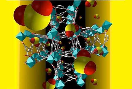
| Sulfur dioxide molecules (red and yellow) are selectively taken up by pores in the metal-organic framework. (Image: Valeriya Chernikova) | |
| Although several lab-based analytical instruments can detect traces of a specific gas in the air, these instruments are typically large, expensive, power-hungry machines. There is still a need for small, inexpensive, energy-efficient sensors that, for example, could be widely deployed around industrial sites to continually monitor air quality. | |
| One promising way to make such sensors involves porous materials called metal-organic frameworks (MOFs). By making the MOF from different metal atoms and organic linkers, researchers can create materials that selectively absorb specific gases into tailor-made pockets within the structure. Two King Abdullah University of Science and Technology (KAUST) research groups, led by materials scientist, Mohamed Eddaoudi, and electronic engineer, Khaled Salama, recently teamed up to develop MOF-based gas sensors. | |
| The first step was completed in 2015 when the team made a proof-of-concept sensor by coating a MOF layer on to an electrode (Sensors, „Insights on Capacitive Interdigitated Electrodes Coated with MOF Thin Films: Humidity and VOCs Sensing as a Case Study”). The device senses gases in a similar way that a touchscreen senses a finger. The gas changes the MOF sensor’s capacitance, an electronic property that can be directly measured using the electrode. | |
| Now, the team is working toward specific applications. “Our current work aims to identify the ideal MOF, in terms of sensitivity and selectivity, for detection of sulfur dioxide,” says Valeriya Chernikova, a Ph.D. student from Eddaoudi’s lab. | |
| The researchers selected an indium-based version of a MOF called MFM-300 as their sensor material. A thin film of the material could be grown onto the electrode under mild conditions that do not damage the sensor circuit. The resulting material forms pockets lined with two -OH groups and four C-H groups that selectively bind sulfur-dioxide molecules. In lab tests using simple mixtures of gases, the sensor could detect sulfur dioxide at concentrations of just a few parts per billion. | |
| To use the technology for real air—which comprises a much more complex mixture of gases—the next step is to develop sensor arrays that pool the responses of multiple MOF materials, Chernikova says. “The data will be processed using various statistical and machine learning algorithms to improve the accuracy of the sensor’s response,” she continues. “This is commonly referred to as an ‘artificial nose’.” |
| Source: King Abdullah University of Science and Technology |
Cercetatorii japonezi au dezvoltat o noua metoda de a construi arii mari de materiale semiconductoare, care are doar doua molecule groase si un total de 4.4 nanometri inaltime.Filmele funcționează ca tranzistori de film subțire și au aplicații potențiale viitoare în electronice flexibile sau detectoare chimice.Proprietățile semiconductoare ale bistratificatorului pot da aplicațiile de filme în electronică flexibilă sau în detectarea chimică.
| Posted: May 03, 2018 | |
Cell membrane inspires new ultrathin electronic film(Nanowerk News) Japanese researchers have developed a new method to build large areas of semiconductive material that is just two molecules thick and a total of 4.4 nanometers tall (Advanced Materials, „Semiconductive single molecular bilayers realized using geometrical frustration”). The films function as thin film transistors, and have potential future applications in flexible electronics or chemical detectors. These thin film transistors are the first example of semiconductive single molecular bilayers created with liquid solution processing, a standard manufacturing process that minimizes costs. |
|
 |
|
| 3D computer model and Atomic Force Microscopy image of the new film made by University of Tokyo scientists. Top surface view of 3D computer model (left) and Atomic Force Microscopy image (right) of the new film made by University of Tokyo scientists. The well-organized structure of the molecules is visible in both the 3D computer model and microscope image as a herringbone or cross-hair pattern. The color differences in the microscopy image are a result of the different lengths of the molecules’ tails; the length differences cause the geometric frustration that prevents layers from stacking. pm = picometers, nm = nanometers. (Image: Shunto Arai and Tatsuo Hasegawa) | |
| „We want to give electronic devices the features of real cell membranes: flexible, strong, sensitive, and super thin. We found a novel way to design semiconductive single molecular bilayers that allows us to manufacture large surface areas, up to 100 square centimeters (39 square inches). They can function as high performance thin film transistors and could have many applications in the future,” said Assistant Professor Shunto Arai, the first author on the recent research publication. | |
| Professor Tatsuo Hasegawa of the University of Tokyo Department of Applied Physics led the team that built the new film. The breakthrough responsible for their success is a concept called geometric frustration, which uses a molecular shape that makes it difficult for molecules to settle in multiple layers on top of each other. | |
| The film is transparent, but the forces of attraction and repulsion between the molecules create an organized, repeated herringbone pattern when the film is viewed from above through a microscope. The overall molecular structure of the bilayer is highly stable. Researchers believe it should be possible to build the same structure out of different molecules with different functionalities. | |
 |
|
| Artist’s representation of geometrically frustrated molecules. The molecules are aligned head-to-head (yellow portions) with their tails pointing in opposite directions (gray portions) so the molecules form a vertical line. The different tail lengths prevent additional layers of molecules from stacking on top. Thin film transistors made of single molecular bilayers will have better device performance than films that are irregular or greater thickness. (Image: The University of Tokyo) | |
| The individual molecules used in the current film are divided into two regions: a head and a tail. The head of one molecule stacks on top of another, with their tails pointing in opposite directions so the molecules form a vertical line. These two molecules are surrounded by identical head-to-head pairs of molecules, which all together form a sandwich called a molecular bilayer. | |
| Researchers discovered they could prevent additional bilayers from stacking on top by building the bilayer out of molecules with different length tails, so the surfaces of the bilayer are rough and naturally discourage stacking. This effect of different lengths is referred to as geometric frustration. | |
| Standard methods of creating semiconductive molecular bilayers cannot control the thickness without causing cracks or an irregular surface. The geometric frustration of different length tails has allowed researchers to avoid these pitfalls and build a 10cm by 10cm (3.9 inches by 3.9 inches) square of their film using the common industrial method of solution processing. | |
 |
|
| Artist’s representation of the blade coating solution process to produce single molecular bilayer thin film transistors. Liquid molecules are spread by a blade over the production surface at room temperature and standard air pressure in a technique called solution processing. As the liquid dries, the inter-molecular forces cause the molecules to automatically arrange themselves into geometrically frustrated single bilayers just 4.4 nanometers thick. (Image: Shunto Arai and Tatsuo Hasegawa) | |
| The semiconductive properties of the bilayer may give the films applications in flexible electronics or chemical detection. | |
| Semiconductors are able to switch between states that allow electricity to flow (conductors) and states that prevent electricity from flowing (insulators). This on-off switching is what allows transistors to quickly change displayed images, such as a picture on an LCD screen. The single molecular bilayer created by the UTokyo team is much faster than amorphous silicon thin film transistors, a common type of semiconductor currently used in electronics. | |
| The team will continue to investigate the properties of geometrically frustrated single molecular bilayers and potential applications for chemical detection. Collaborators based at the National Institute of Advanced Industrial Science and Technology, the Nippon Kayaku Company Limited, Condensed Matter Research Center, and High Energy Accelerator Research Organization also contributed to the research. |
| Source: University of Tokyo |
raporteaza informatii importante despre aurul nanoporos – un material cu aplicatii in crestere in mai multe domenii, incluzand dispozitive de stocare a energiei si dispozitive biomedicale – fara a intra intr-un laborator.Nanoporous aur a fost studiat de aproximativ 15 ani, dar putin este de fapt cunoscut despre caracteristicile sale fizice si limitele de tunability sale pentru aplicatii specifice, echipa scrie in rapoartele stiintifice .
| Posted: May 03, 2018 | |
Mining for nanogold with a computer(Nanowerk News) Engineers from Texas A&M University and Virginia Tech report important new insights into nanoporous gold–a material with growing applications in several areas, including energy storage and biomedical devices–all without stepping into a lab. |
|
| Instead of conducting any additional experiments, the team used image-analysis software developed in-house to „mine” the existing literature on nanoporous gold (NPG). Specifically, the software analyzed photographs of NPG from some 150 peer-reviewed papers, quickly measuring key features of the material that the researchers then correlated with written descriptions of how the samples were prepared. One of the results? A recipe, of sorts, for how to make NPG with specific characteristics. | |
| „We were able to back out a quantitative law that explains how you can change NPG features by changing the processing times and temperatures,” said Ian McCue, a postdoctoral researcher in the Texas A&M Department of Materials Science and Engineering. McCue is lead author of a paper on the work published in Scientific Reports („Gaining new insights into nanoporous gold by mining and analysis of published images”). | |
 |
|
| These images show some of the physical characteristics of nanoporous gold at different magnifications. (Image: Texas A&M University) | |
| The team also identified a new parameter related to NPG that could be used to better tune the material for specific applications. | |
| „Before our work, engineers knew of one tunable ‘knob’ for NPG. Now we have a second one that could give us even more control over the material’s properties,” said Josh Stuckner, a graduate student at Virginia Tech and co-author of the paper. Stuckner developed the software that allowed the new insights. | |
| Other authors are Dr. Michael J. Demkowicz, associate professor in the materials science and engineering department at Texas A&M, and Dr. Mitsu Murayama, associate professor at Virginia Tech. | |
| Nanoporous gold has been studied for some 15 years, but little is actually known about its physical characteristics and the limits of its tunability for specific applications, the team writes in Scientific Reports. | |
| The material is a three-dimensional porous network of interweaving strands, or ligaments. Multiple ligaments, in turn, connect at points called nodes. All of these features are almost unimaginably small. Stuckner notes, for example, that some of the smaller pores would fit about three strands of DNA side by side. As a result, McCue said the overall structure is very complex and it’s been extremely difficult and time-consuming to measure features like the lengths between nodes and the diameters of ligaments. But Stuckner’s software has changed that. | |
| „Manually it might take 20 minutes to over an hour to measure the features associated with one image,” Stuckner said. „We can do it in a minute, or even just tell the computer to measure a whole slew of images while we walk away.” | |
| Earlier attempts to measure NPG features led to very small data sets of five or six data points. The Texas A&M/Virginia Tech team has looked at around 80 data points. That, in turn, allowed the team to create the new quantitative description of NPG features associated with different processing techniques. All that without doing any actual experiments, just clever data-mining and analysis, said McCue. | |
| The work has also led to new publication guidelines for future researchers. Of the 2,000 papers the team originally analyzed, only 150 had useful information. | |
| „We had to throw out a lot of data due to poor image quality or a lack of written information on how a given NPG was processed,” McCue said. „The new guidelines could prevent that, ultimately allowing better data mining not only for NPG but for other materials.”
Source: By Elizabeth Thomson, Texas A&M University |
unei noi clase de catalizatori atomici unici (SAC) susținute pe nanotuburi de carbon care prezintă o reducere electrochimică remarcabilă a CO 2 la CO. % pentru clasa nouă, nanotuburile de carbon cu azot dopat de azot, cu un atom de azot (NiSA-N-CNT), se consideră a fi cea mai mare încărcare de metal pentru SAC-urile raportate până în prezent.
Atomii atomici de nichel, cobalt și fier au fost sprijiniți pe nanotuburi de carbon dopate cu azot printr-o metodă de piroliză cu un singur recipient și comparate în studiu.Noua clasă de SAC are un potențial extraordinar, cu aplicații promițătoare în domeniile electrocatalizei și catalizatorilor pentru conversia energiei, precum și a altor utilizări;au dezvoltat un nou proces de sinteză și dezvoltare a nanotuburilor de carbon dopate cu azot cu un ligand de nichel care demonstrează activitate catalitică ridicată.
| Posted: May 02, 2018 | |
New class of single atoms catalysts for carbon nanotubes exhibit outstanding electrochemical reduction of CO2 to CO(Nanowerk News) Experiments using X-rays on two beamlines at the Australian Synchrotron have helped characterise a new class of single atom catalysts (SACs) supported on carbon nanotubes that exhibit outstanding electrochemical reduction of CO2 to CO. A weight loading of 20 wt% for the new class, nickel single atom nitrogen doped carbon nanotubes (NiSA-N-CNTs), is believed to be the highest metal loading for SACs reported to date. |
|
| Single atoms of nickel, cobalt and iron were supported on nitrogen doped carbon nanotubes via a one-pot pyrolysis method and compared in the study. | |
| A large international collaboration, led by Prof San Ping Jiang, Deputy Director of the Fuels and Energy Technology Institute at the Curtin University of Technology and associates from the Department of Chemical Engineering, have developed a new synthesis and development process for nitrogen-doped carbon nanotubes with a nickel ligand that demonstrate high catalytic activity. | |
| The study was published in Advanced Materials („Atomically Dispersed Transition Metals on Carbon Nanotubes with Ultrahigh Loading for Selective Electrochemical Carbon Dioxide Reduction”) and featured on the inside cover of the publication. | |
| Dr Bernt Johannessen, instrument scientist on the X-ray absorption spectroscopy (XAS) beamline at the Australian Synchrotron was a co-author on the paper, which also included lead investigators from Curtin University of Technology and collaborators at the University of Western Australia, Institute of Metal Research (China), Oak Ridge National Laboratory (US), University of the Sunshine Coast, University of Queensland, Tsinghua University (China) and King Abdulaziz University (Saudi Arabia). Technical support and advice on the soft X-ray spectroscopy experiments was provided by Australian Synchrotron instrument scientist Dr Bruce Cowie. | |
| “The whole idea behind the approach is that the smaller particles you have, the more catalytically active they are. As you go to a nanoparticle size, you see catalytic activity increase. And if you take that to the extreme, you are looking at single metal atoms anchored on a supporting substrate of carbon,” said Johannessen. | |
| “Because surface atoms behave differently to bulk or other atoms, XAS was used to verify there were in fact single atoms and the position of those nickel atoms relative to other atoms. We were able to determine bond lengths and coordination numbers.” | |
| The adding or subtracting single atoms from a particle opens up the possibility of tuning its properties. | |
| The challenge has been to keep the metal atoms, which provide a strong metal support bond, from interacting with each other and aggregating because of their higher surface energy. | |
| The investigators overcame this by developing a multistep method to synthesise atomically dispersed nickel atoms on nitrogen doped CNTs that included decomposing the precursor solution at high temperature. | |
| The X-ray absorption near edge structure spectroscopy (XANES) measurements at the Australian Synchrotron provided supporting evidence of the electrochemical efficiency of NiSA-N-CNTs. The results suggested that the Ni-N species are the active centres for the reduction reaction of CO2 to CO. The single nickel atoms are held by coordinating nitrogen atoms in the N- doped carbon nanotube structure and this helps stabilise the structure from metal aggregation. | |
| The NiSA-N-CNTs also demonstrated a higher turnover frequency than other nitrogen doped CNTs. The data confirmed there was no obvious aggregation or breakdown of nickel and also revealed the structural durability of the NiSA-N-CNTs as electrocatalysts. | |
| A number of other techniques and simulations were undertaken as part of materials characterisation and to confirm the CO2 reaction reduction. | |
| The new class of SACs has tremendous potential with promising applications in the areas of electrocatalysis and catalysts for energy conversion as well as other uses. |
| Source: Australian Synchrotron |
Pulsul generat de laserul cu matrice nanoparticule este atât de rapid încât nu există camere electronice convenționale care să-și poată capta dinamica. Cercetatorii au folosit un alt laser ca o „camera”, facand fotografii foarte rapide ale laserului mic. Metoda se numește spectroscopie sonda pompă.
| Posted: May 02, 2018 | |
Ultrafast laser pulse created by golden nanoparticles(Nanowerk News) A new study shows that organic dye material combined with metallic nanostructures can provide ultrafast lasing dynamics with short and rapidly appearing laser pulses (Nano Letters, „Ultrafast Pulse Generation in an Organic Nanoparticle-Array Laser”). |
|
| ‘We wanted to find out how fast we can turn our laser device on and off. Generating laser pulses quickly can be very useful in information processing and can improve the response of some optoelectronic devices,’ explains postdoctoral researcher Konstantinos Daskalakis at Aalto University. | |
| The samples used in the experiments are made out of gold nanoparticles placed on glass and immersed in an organic, light-emitting material. The nanoparticles are arranged very close to each other in a square array. Electric fields localised around the particles result in high field strengths that speed up the molecular dynamics in the organic dye. | |
 |
|
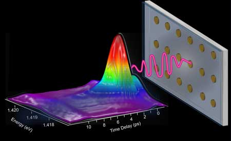
| Illustration of the nanoparticle-array laser generating one-trillionth-of-a-second-long laser pulses. (Image: Konstantinos Daskalakis) | |
| The electromagnetic fields and the conducting gold particles interact both with each other and the organic dye to generate a directional laser pulse that is ultrafast, one trillionth of a second long. | |
| Generating a laser of this kind is promising for all-optical switching and sensing and will potentially improve the speed of optical telecommunications and performance of devices that use light to process information, such as cameras and transistors. | |
| Very small nanolasers do not usually provide clearly directional beams. Arranging nanoparticles in an array considerably improves directionality. Such lasers have already been created in several laboratories in the world, but their potential for ultrafast pulses has not been proven before the experiments conducted at Aalto University. | |
| Measuring the properties of the pulses is very demanding because of their tremendous speed. | |
| ‘The key achievement here is that we have succeeded in experimentally demonstrating that the laser pulses are indeed ultrafast. The lasing occurs in optical modes that are hybrids of light and the motion of electrons in metal. These modes are called surface lattice resonances,’ explains Academy Professor Päivi Törmä. | |
| The laser light is first squeezed by the metallic nanoparticles into sub-wavelength dimensions, and then it escapes from the surface lattice resonance modes as a picosecond-fast, concentrated laser pulse. | |
| ‘These kinds of metal nanoparticle array lasers are excellent for generating pulsed laser radiation with a high modulation speed,’ says doctoral student Aaro Väkeväinen. | |
| The pulse generated from the nanoparticle-array laser is so fast that there are no conventional electronic cameras that can capture its dynamics. The researchers used another laser as a “camera”, taking very fast pictures of the tiny laser. The method is called pump-probe spectroscopy. |
| Source: Aalto University |
Retina artificială constă într-o peliculă subțire circulară de material fotoactiv și este similară cu un pixel individual într-un senzor de cameră digitală. Fiecare pixel este cu adevărat microscopic – este de aproximativ 100 de ori mai subțire decât o singură celulă și are un diametru mai mic decât diametrul părului uman. Se compune dintr-un pigment de nanocristale semiconductoare. Astfel de pigmenți sunt ieftini și non-toxici și sunt utilizați în mod obișnuit în cosmeticele comerciale și în cerneala tatuajelor.
| Posted: May 02, 2018 | |
Organic printing nanoinks may restore sight to blind people(Nanowerk News) A simple retinal prosthesis is being developed in collaboration between Tel Aviv University in Israel and Linköping University in Sweden. Fabricated using cheap and widely-available organic pigments used in printing inks and cosmetics, it consists of tiny pixels like a digital camera sensor on a nanometric scale. Researchers hope that it can restore sight to blind people. |
|
| Researchers led by Eric Glowacki, principal investigator of the organic nanocrystals subgroup in the Laboratory of Organic Electronics, Linköping University, have developed a tiny, simple photoactive film that converts light impulses into electrical signals. These signals in turn stimulate neurons (nerve cells). The research group has chosen to focus on a particularly pressing application, artificial retinas that may in the future restore sight to blind people. | |
| The Swedish team, specializing in nanomaterials and electronic devices, worked together with researchers in Israel, Italy and Austria to optimise the technology. Experiments in vision restoration were carried out by the group of Yael Hanein at Tel Aviv University in Israel. Yael Hanein’s group is a world-leader in the interface between electronics and the nervous system. | |
| The results have recently been published in Advanced Materials („Direct electrical neurostimulation with organic pigment photocapacitors”). | |
 |
|
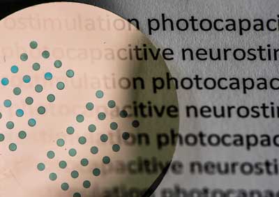
| An array of semitransparent organic pixels on top of a ultrathin sheet of gold. The thickness of both the organic islands and the underlying gold is more than one-hundred times thinner than a single neuron. (Image: Thor Balkhed) | |
| The retina consists of several thin layers of cells. Light-sensitive neurons in the back of the eye convert incident light to electric signals, while other cells process the nerve impulses and transmit them onwards along the optic nerve to an area of the brain known as the “visual cortex”. An artificial retina may be surgically implanted into the eye if a person’s sight has been lost as a consequence of the light-sensitive cells becoming degraded, thus failing to convert light into electric pulses. | |
| The artificial retina consists of a thin circular film of photoactive material, and is similar to an individual pixel in a digital camera sensor. Each pixel is truly microscopic – it is about 100 times thinner than a single cell and has a diameter smaller than the diameter of a human hair. It consists of a pigment of semi-conducting nanocrystals. Such pigments are cheap and non-toxic, and are commonly used in commercial cosmetics and tattooing ink. | |
| “We have optimised the photoactive film for near-infrared light, since biological tissues, such as bone, blood and skin, are most transparent at these wavelengths. This raises the possibility of other applications in humans in the future,” says Eric Glowacki. | |
| He describes the artificial retina as a microscopic doughnut, with the crystal-containing pigment in the middle and a tiny metal ring around it. It acts without any external connectors, and the nerve cells are activated without a delay. | |
| “The response time must be short if we are to gain control of the stimulation of nerve cells,” says David Rand, postdoctoral researcher at Tel Aviv University. “Here, the nerve cells are activated directly. We have shown that our device can be used to stimulate not only neurons in the brain but also neurons in non-functioning retinas.” | |
| Eric Glowacki and his research group work at the Laboratory of Organic Electronics in Norrkoping, Sweden. The research group is part of a larger research initiative called the Wallenberg Center for Molecular Medicine, WCMM, at Linköping University. This initiative has created the unique environment necessary to develop this technology in a collaboration between nanomaterials scientists, biomedical engineers, and biologists. |
| Source: Linköping Universitet |