Arhitecturile grafene moleculare văd lumina

Pe suprafețele plane plate ale unui substrat cu diamant acoperit cu grafen, moleculele se auto-asamblează în arhitectura țintă într-un mod asemănător cu proteinele și nanotehnologia ADN-ului. Singura forță motrice provine din interacțiunile supramoleculare construite prin legături de hidrogen. Asa cum era de asteptat, reteaua moleculara produce o fotocurent atunci cand este expusa la lumina.

Posted: Mar 02, 2016

Molecular graphene architectures see the light

(Nanowerk News) Organic photovoltaics bear great potential for large-scale, cost-effective solar power generation. One challenge to be surmounted is the poor ordering of the thin layers on top of the electrodes. Utilizing self-assembly on atomically flat, transparent substrates, a team of scientists at the Technical University of Munich (TUM) has engineered ordered monolayers of molecular networks with photovoltaic responses. The findings open up intriguing possibilities for the bottom-up fabrication of optoelectronic devices with molecular precision.

Nature is unrivaled when it comes to the self-assembly of complex, high-performance molecular machinery for light absorption, exciton or charge separation and electron transfer. Molecular nanotechnologists have long dreamt of mimicking such extraordinary biomolecular architectures and rewiring them to produce inexpensive electricity.
Now researchers from the Departments of Physics and Chemistry at the Technical University of Munich (TUM), from the Max-Planck Institute for Polymer Research (Mainz, Germany) and the Université de Strasbourg (France) have modified dye molecules in such a manner that allows them to serve as building blocks of self-assembling molecular networks (Nature Communications, „Photoresponse of supramolecular self-assembled networks on graphene-diamond interfaces”).
On the atomically flat surfaces of a graphene coated diamond substrate the molecules self-assemble into the target architecture in a manner akin to proteins and DNA nanotechnology. The sole driving force stems from the engineered supramolecular interactions via hydrogen bonds. As expected, the molecular network produces a photocurrent when exposed to light.
Scanning tunneling microscopic topography of melamine linked terrylene-diimide molecules with inserted model of the molecular nertwork
Scanning tunneling microscopic topography of melamine linked terrylene-diimide molecules with inserted model of the molecular nertwork (Scale bar: 2nm). (Image: C. A. Palma / TUM)
From art to application
“For a long time engineered self-assembled molecular architectures were looked upon as arty,” says PD Dr. Friedrich Esch, a lead author of the study. “With this publication we present for the first time a serious practical implementation of this technology.”
“In conventional organic photovoltaics the improvement of molecular order is still a challenge. In contrast, the nanotechnology toolbox provides us with the possibility of an atomically precise layout of the constituting components a priori,” says Dr. Carlos-Andres Palma, who co-supervised the study. “The possibility of full physicochemical control of the components gives us additional set-screws for functional optimization.”
The scientists now hope to scale up the device configuration and certify the photovoltaic response under standard conditions. “Intercalating self-assembled dyes between stacks of two-dimensional electrodes like graphene, opens up the possibility of easy scale-up to efficient photovoltaic monolayer elements”, claims Dr. Palma “This will put our work on the solar cell technology map”.
Perfect match of surface chemistry and physics
The scientists used terrylene-diimide molecules as photoactive dyes. The network is formed when the elongated terrylene molecules link up with trivalent melamine. By choosing adequate side groups for the terrylene diimide the authors of the study determine which architectures can form.
“This work is an excellent example of the interdisciplinary cooperation we seek to initiate with the institution of the Catalysis Research Center: a perfect match of chemistry and physics,” says Professor Ulrich Heiz, director of the TUM Catalysis Research Center.
Source: Technical University of Munich

Read more: Molecular graphene architectures see the light

Caracterizarea cuantică a luminii Hall cu zoom în jurul unui cip fotonic

Cercetătorii au elaborat un comportament cuantic în alte platforme, pe lângă domeniul solidar în care a fost descoperit inițial. Semnăturile unei astfel de fizici au fost observate în gazele atomice ultravold și în fotoni, unde lumina se deplasează în chipsuri fabricate. Hafezi și colegii au condus acuzația în domeniul fotonicii.
Grupul utilizează un cip pe bază de siliciu care este umplut cu o serie de structuri în formă de inel numite rezonatoare. Rezonatorii sunt conectați între ei prin intermediul ghidurilor de undă.
Designul cipului determină strict condițiile în care lumina poate călători de-a lungul marginilor, mai degrabă decât prin regiunile interioare. Cercetatorii masoara spectrul de transmitere, care este fractia de lumina care trece cu succes printr-o cale margine. Pentru a circula fără obstacole prin modurile protejate de margini, lumina trebuie să posede o anumită energie. Transmisia crește atunci când energia luminoasă corespunde acestui criteriu.

Posted: Mar 02, 2016

Characterizing quantum Hall light zooming around a photonic chip

(Nanowerk News) When it comes to quantum physics, light and matter are not so different. Under certain circumstances, negatively charged electrons can fall into a coordinated dance that allows them to carry a current through a material laced with imperfections. That motion, which can only occur if electrons are confined to a two-dimensional plane, arises due to a phenomenon known as the quantum Hall effect.

Researchers, led by Mohammad Hafezi, a JQI Fellow and assistant professor in the Department of Electrical and Computer Engineering at the University of Maryland, have made the first direct measurement that characterizes this exotic physics in a photonic platform.
The research was published online Feb. 22 and featured on the cover of the March 2016 issue of Nature Photonics („Measurement of Topological Invariants in a 2D Photonic System”). These techniques may be extended to more complex systems, such as one in which strong interactions and long-range quantum correlations play a role.
text
Image of photonic chip and apparatus. (Image: E. Edwards/JQI)
The quantum Hall effect is best understood by peering through the lens of topology. In the 1980s, physicists discovered that electrons in some materials behave strangely when subjected to large magnetic fields at extreme cryogenic temperatures. Remarkably, the electrons at the boundary of the material will flow along avenues of travel called ‘edge states’, protected against defects that are most certainly present in the material.
Moreover, the conductance–a measure of the current–is quantized. This means that when the magnetic field is ramped up, then the conductance does not change smoothly. Instead it stays flat, like a plateau, and then suddenly jumps to a new value. The plateaus occur at precise values that are independent of many of the material’s properties. This hopping behavior is a form of precise quantization and is what gives the quantum Hall effect its great utility, allowing it to provide the modern standard for calibrating resistance in electronics, for instance.
Researchers have engineered quantum Hall behavior in other platforms besides the solid-state realm in which it was originally discovered. Signatures of such physics have been spotted in ultracold atomic gases and photonics, where light travels in fabricated chips. Hafezi and colleagues have led the charge in the photonics field.
The group uses a silicon-based chip that is filled with an array of ring-shaped structures called resonators. The resonators are connected to each other via waveguides.
The chip design strictly determines the conditions under which light can travel along the edges rather than through the inner regions. The researchers measure the transmission spectrum, which is the fraction of light that successfully passes through an edge pathway. To circulate unimpeded through the protected edge modes, the light must possess a certain energy. The transmission increases when the light energy matches this criteria.
For other parameters, the light will permeate the chip interior or get lost, causing the transmission signal to decrease. The compiled transmission spectrum looks like a set of bright stripes separated by darker regions (see figure). Using such a chip, this group previously collected images of light traveling in edge states, definitively demonstrating the quantum Hall physics for photons.
In this new experiment Hafezi’s team modified their design to directly measure the value of the topology-related property that characterizes the photonic edge states. This measurement is analogous to characterizing the quantized conductance, which was critical to understanding the electron quantum Hall effect. In photonics, however, conductance is not relevant as it pertains to electron-like behavior. Here the significant feature is the winding number, which is related to how light circulates around the chip. Its value equals to the number of available edge states and should not change in the face of certain disruptions.
To extract the winding number, the team adds 100 nanometer titanium heaters on a layer above the waveguides. Heat changes the index of refraction, namely how the light bends as it passes through the waveguides. In this manner, researchers can controllably imprint a phase shift onto the light. Phase can be thought of in terms of a time delay. For instance, when comparing two light waves, the intensity can be the same, but one wave may be shifted in time compared to the other. The two waves overlap when one wave is delayed by a full oscillation cycle—this is called a 2π phase shift.
text
(click on image to enlarge)
On the chip, enough heat is added to add a 2π phase shift to the light. The researchers observe an energy shift in the transmission stripes corresponding to light traveling along the edge. Notably, in this chip design, the light can circulate either clockwise (CW) or counterclockwise (CCW), and the two travel pathways do not behave the same (in contrast to an interferometer). When the phase shift is introduced, the CW traveling light hops one direction in the transmission spectrum, and the CCW goes the opposite way. The winding number is the amount that these edge-state spectral features move and is exactly equivalent to the quantized jumps in the electronic conductance.
Sunil Mittal, lead author and postdoctoral researcher explains one future direction, “So far, our research has been focused on transporting classical [non-quantum] properties of light–mainly the power transmission. It is intriguing to further investigate if this topological system can also achieve robust transport of quantum information, which will have potential applications for on-chip quantum information processing.”
Background: Symmetry and Topology
Physicists use different approaches to classify matter; symmetry is one powerful method. For instance, the microscopic structure of a material like diamond looks the same even while shifting your gaze to a new spot in the crystal. These symmetries – the rotations and translations that leave the microscopic structure the same – predict many of the physical properties of crystals.
Symmetry can actually offer a kind of protection against disruptions. Here, the word protection means that the system (e.g. a quantum state) is robust against changes that do not break the symmetry. Recently, another classification scheme based on topology has gained significant attention. Topology is a property that depends on the global arrangement of particles that make up a system rather than their microscopic details. The excitement surrounding this mathematical concept has been driven by the idea that the topology of a system can offer a stability bubble around interesting and even exotic physics, beyond that of symmetry. Physicists are interested in harnessing states protected by both symmetry and topology because quantum devices must be robust against disturbances that can interfere with their functionality.
Source: Joint Quantum Institute

Read more: Characterizing quantum Hall light zooming around a photonic chip

Respectarea cerințelor de performanță crescătoare la frecvențele cu valuri milimetrice

dezvolta funcționalitatea complementară a materialului semiconductor compus (III-V CMOS), care susține atât funcționalitatea analogică, cât și cea digitală în domeniul frecvențelor undei milimetrice. Nivelele III-V vor fi folosite pentru a menține controlul electrostatic, deoarece lungimea porții este redusă pentru nodurile tehnologice viitoare. Secțiunea transversală mică a nanofirelor facilitează în continuare integrarea pe substraturile cu ajutorul nanotehnologie

Posted: Mar 02, 2016

Meeting the increasing performance demands at millimetre-wave frequencies

(Nanowerk News) Future radar imaging systems and 5G communication systems will generate improved resolution and provide higher data-transmission rates when operated at higher frequencies, but at the cost of increased power consumption. To reduce power consumption, increase performance, and lower costs, the European project INSIGHT (Integration of III-V Nanowire Semiconductors for Next Generation High Performance CMOS SOC Technologies) is aiming at developing III-V CMOS (complementary metal-oxide-semiconductor) technology. The six partners, including universities, research institutes and one company, are committed to establishing a manufacturable III-V CMOS technology on Si substrates, to reduce costs and to save scarce materials.

The INSIGHT mission is to develop complementary functionality in compound semiconductor material (III-V CMOS), supporting both analogue and digital functionality in the millimetre-wave frequency domain. III-V nanowires will be used to maintain electrostatic control, as the gate length is scaled for future technology nodes. The small nanowire cross-section further facilitates the integration onto Si substrates using nanotechnology.
“The fabrication of high-performance III-V components on large Si substrates using CMOS compatible technologies opens a path for cost reduction of millimetre-wave key components with minimized usage of critical materials” says Lars-Erik Wernersson, Professor at Lund University and coordinator for INSIGHT. Lund University is coordinating this new European Horizon 2020 research project that has been funded with 4.3 million Euros over 36 months.
Professor Lars-Erik Wernersson from Lund University, introducing the INSIGHT project.
IBM foresees a growing need to push the limits of chip technology to meet the emerging demands of cognitive computers, Internet of Things and Cloud platforms, due to the enormous amount of data they are handling – 90% of which is unstructured. The new technology developed in INSIGHT offers a potential solution to scale chip technology beyond the 10 nm node as well as opening up a range of new application areas. Integrating III-V materials into Si CMOS can enable better logic circuits with a lower power consumption, and in addition can enable the realization of System-on-Chip (SoC) products taking full advantage of III-V’s state-of-the-art RF/Analog metrics.
There is a growing need for performance enhancements of key components in the millimetre-wave frequency range and new consumer applications are demanding low costs. The new technology offers a potential solution, as it may provide both high-performance analogue and digital functionality on the same platform where the improved manufacturability allows production on larger wafers. The INSIGHT consortium addresses the technology need with the ambition to demonstrate circuits and systems by optimizing both material and device properties.
The introduction of III-V materials on silicon substrates by using nanowires is one of the most innovative heterogeneous integration approaches today. Fraunhofer
IAF will bring in their III-V process and circuit design experience, and is interested in transferring the results and findings to next generation III-V device technologies.
The LETI participation in the INSIGHT project involves both the Silicon Component division and the Integrated Circuit & Embedded System division, ranging from materials to the circuit demonstration. The technology expands the LETI platform for smart devices and Internet of Things with the potential to squeeze multiple functions into a single die.
III-V CMOS technology may be particularly suited for millimetre-wave front-ends where it will be used to detect and generate signals for communication, radar and imaging. It is the goal of the INSIGHT consortium to develop key technologies for both the receivers and transmitters, while exploring the limits of the transistor geometry and layout.
Besides Fraunhofer IAF (Germany) and LETI (France), the consortium consists of Lund University (Sweden), University of Glasgow (UK), Tyndall National Institute (Ireland) and IBM (Switzerland). The expertise of the partners spans the complete spectrum from materials, through devices, all the way to circuits and systems, allowing the consortium to take this promising technology further along the path to commercial products. INSIGHT is funded under the Horizon 2020 Programme for Research and Development of the European Union (Grant agreement number 688784).
Source: Project INSIGHT

Read more: Meeting the increasing performance demands at millimetre-wave frequencies

Spinning mai bine dispozitive electronice

Folosind o combinație de pulverizare (pentru metale) și depunere pulsată cu laser (pentru izolator), am arătat cu succes că izolatorul magnetic cu grosimea de 50-100 nanometri, cum ar fi granat de fier de ytriu, nu este numai magnetic și izolator, Este cultivată pe platină de 5 nanometri grosime.

Posted: Mar 02, 2016

Spinning better electronic devices

(Nanowerk News) A team of researchers, led by a group at the University of California, Riverside, have demonstrated for the first time the transmission of electrical signals through insulators in a sandwich-like structure, a development that could help create more energy efficient electronic devices.

Jing Shi, University of California - Riverside
Jing Shi, a professor of physics.
Conventional electronic devices rely on the transport of electrons in a semiconductor such as silicon. Now, researchers are exploiting the ‘spin’ of the electron rather than its charge to create a new generation of ‘spintronic’ devices that are potentially more energy efficient and more versatile than those currently making up silicon chips and circuit elements.The UC Riverside-led research, which was published online Wednesday (March 2) in the journal Nature Communications („Observation of magnon-mediated current drag in Pt/yttrium iron garnet/Pt(Ta)trilayers”), is significant because it demonstrates that a tri-layer, sandwich-like, structure can serves as a scalable pure spin current device, an essential ingredient in spintronics.

A key element in this breakthrough is the material. To demonstrate the effect, the magnetic insulator needs to be truly insulating, or there will be a parasitic signal from leakage. On the other hand, a high-quality magnetic insulator grown on metal had never been demonstrated.

Using combination of sputtering (for metals) and pulsed laser deposition (for insulator), we successfully showed that the 50-100 nanometer thick magnetic insulator, such as yttrium iron garnet, is not only magnetic and insulating, but also of high quality when it is grown on 5 nanometer thick platinum.
In the structures used by the researchers, there are two metals and a magnetic insulator in between. The metals are for spin current generation and detection (conversion of spin current back to charge current) via the so-called spin Hall effect and inverse spin Hall effect.
The magnetic insulator is an electrical insulator but a good spin current conductor. The spin current flowing in the insulator does not involve mobile electrons therefore it does not dissipate energy as an electrical current does in joule heating.
The researchers have also demonstrated that the signal transmission can be switched on and off and modulated in its strength by a magnetic field. The electrical signal transmission through the magnetic insulators can be switched on and off depending on the magnetic state, or direction of the magnetization, of the magnetic insulators.
So the direction of the magnetization can be regarded as a memory state of non-volatile random access memory devices. In addition, the signal level can be modulated by changing the direction of the magnetization; therefore, it can also be used as analog devices. The sandwich structure can be made small by nanofabrication so that the devices can be scaled down.
Source: University of California – Riverside

Read more: Spinning better electronic devices

Cercetătorii au șanse pentru noi materiale optoelectronice 2-D

Studiul lor oferă o platformă pentru ingineria materialelor bidimensionale (2D) cu proprietăți optice și electronice care depind puternic de configurațiile de stivuire. Constatările sunt publicate în ACS Nano („Twisted MoSe2 Bilayers cu stivuire variabilă locală și cuplaj interlayer dezvăluit de spectrometrie Raman de joasă frecvență”).

Posted: Mar 02, 2016

Researchers stack the odds for novel optoelectronic 2-D materials

(Nanowerk News) Stacking layers of nanometer-thin semiconducting materials at different angles is a new approach to designing the next generation of energy-efficient transistors and solar cells. The atoms in each layer are arranged in hexagonal arrays. When two layers are stacked and rotated, atoms from one layer overlap with those in the other layer and can form an infinite number of overlapping patterns, like the Moiré patterns that result when two screens are overlaid and one is rotated on top of the other. Theoretical calculations predict excellent electronic and optical properties for some stacking patterns, but practically, how can these patterns be made and characterized?

Recently a team led by researchers from the Department of Energy’s Oak Ridge National Laboratory used the vibrations between two layers to decipher their stacking patterns. The team employed a method called low-frequency Raman spectroscopy to measure how the layers vibrate with respect to each other and compared the frequencies of the measured vibrations with their theoretically predicted values. Their study provides a platform for engineering two-dimensional (2D) materials with optical and electronic properties that strongly depend on stacking configurations. The findings are published in ACS Nano („Twisted MoSe2 Bilayers with Variable Local Stacking and Interlayer Coupling Revealed by Low-Frequency Raman Spectroscopy”).
Stacked Semiconductor
Mutual rotation of two monolayers of a semiconducting material creates a variety of bilayer stacking patterns, depending on the twist angle. Fast and efficient characterization of these stacking patterns may aid exploration of potential applications in electronics and optoelectronics. (Image: ORNL)
„Low-frequency Raman spectroscopy, in combination with first-principles modeling, offers a quick and easy approach to reveal complex stacking configurations in the twisted bilayers of a promising semiconductor, without relying on other expensive and time-consuming experimental techniques,” said co-lead author Liangbo Liang, a Wigner Fellow at ORNL. „We are the first to show that low-frequency Raman spectra can be used as fingerprints to characterize the relative layer stacking in semiconducting 2D materials.”
In Raman scattering, an optical method for probing atomic vibrations, a material scatters monochromatic light from a laser. Whereas conventional Raman spectroscopy may probe more than approximately 3 trillion atomic vibrations per second, low-frequency Raman spectroscopy detects vibrations that are an order of magnitude slower. The low-frequency technique is sensitive to weak attractive forces between layers, called van der Waals coupling. It can provide crucial insight about layer thickness and stacking–aspects that govern fundamental properties of 2D materials.
„This work combines state-of-the art synthesis and processing of 2D materials, their unique spectroscopic characterization, and data interpretation using first-principles theory,” said co-lead author Alex Puretzky. „High-resolution Raman spectroscopy that can probe low-frequency modes requires specialized instrumentation, and only a few places around the world have such a capability together with advanced synthesis and characterization tools, and theory and computational modeling expertise. The Center for Nanophase Materials Sciences at ORNL is among them.”
Chemical vapor deposition, widely employed to synthesize 2D materials like graphene, was used to make perfectly triangular crystal monolayers of molybdenum diselenide just three atoms thick. Feedstock molecules of molybdenum oxide and sulfur were reacted in a flowing gas within a high-temperature furnace to form the triangular crystals on silicon substrates.
„Numerous parameters need to be properly adjusted to synthesize large, triangular 2D crystals successfully,” Puretzky said. „Then, carefully removing the crystals and stacking them precisely in different orientations is a big challenge.”
He continued, „The precise, equilateral triangular shape of the synthesized and transferred crystals allowed us to measure the twist angles with a high precision using standard optical and atomic force microscopy images, which was a key factor in our experiments.”
Theoretical and computational aspects were challenging too. „Raman spectroscopy is heavily based on theory for interpretation and assignment of the observed Raman spectra, especially for new materials that have never before been measured,” Puretzky said.
The study revealed patterns in the stacked bilayers that strongly depend on the twist angle. Some specific twist angles, though, showed periodically repeating patches with the same stacking orientation. „These unique patterns may provide a new platform for optoelectronic applications of these materials,” Puretzky said.
The team’s findings also showed fascinating effects of the vibrations between the layers. As different stacking patterns appeared when layers were displaced, variable spacings occurred between the layers at some specific twist angles. The researchers plan further measurements and modeling for different stacking configurations to better understand how these vibrational decays might alter the thermal properties of these materials–knowledge that could affect applications in heat dissipation and thermoelectric energy conversion.
Source: Oak Ridge National Laboratory

Read more: Researchers stack the odds for novel optoelectronic 2-D materials

Separarea metamaterialelor propusă pentru utilizări chimice, biomoleculare

cercetatorii cred ca manipularea transferului de masa folosind metamaterialele ar putea ajuta la reducerea energiei necesare pentru anumite procese chimice si biomoleculare. Tehnica propusă ar folosi materiale polimerice cu model special pentru a direcționa fluxul atomilor prin folosirea proprietăților lor fizice specifice.
O explicație detaliată a modului în care tehnica ar putea fi utilizată pentru a separa un amestec de azot și oxigen – prin mascarea azotului și concentrarea oxigenului

Posted: Mar 02, 2016

Metamaterial separation proposed for chemical, biomolecular uses

(Nanowerk News) The unique properties of metamaterials have been used to cloak objects from light, and to hide them from vibration, pressure waves and heat. Now, a Georgia Institute of Technology researcher wants to add another use for metamaterials: creating a new directional separation technique that cloaks one compound while concentrating the other. Though the idea must still be proven experimentally, the researchers believe that manipulating mass transfer using metamaterials could help reduce the energy required for certain chemical and biomolecular processes. The proposed technique would use specially-patterned polymeric materials to direct the flow of atoms by taking advantage of their specific physical properties.

A detailed explanation for how the technique could be used to separate a mixture of nitrogen and oxygen – by cloaking the nitrogen and concentrating the oxygen – was reported February 25 in the journal Scientific Reports („Mass Separation by Metamaterials”). The research was supported by a seed grant from the American Chemical Society.
Concentration profiles for concentrated compound B at different times and steady-state
Concentration profiles for concentrated compound B at different times and steady-state. (a–e) background, (f–j) anisotropic homogeneous concentrator, (k–o) multilayer concentrator. (Credit: Martin Maldovan and Juan Manuel Restrepo-Flórez, Georgia Tech)
„We will control how the atoms cross the metamaterial, in which direction they will go,” said Martin Maldovan, an assistant professor in Georgia Tech’s School of Chemical & Biomolecular Engineering and School of Physics. „By designing the diffusivity of the metamaterials, we can make the atoms of one compound go one way, and the atoms of another compound go a different way. We are manipulating the physical properties to control the direction the atoms take through the metamaterial shell.”
Maldovan and Graduate Research Assistant Juan Manuel Restrepo-Flórez have evaluated their metamaterial using computational techniques, and plan to build a prototype separation device this summer. The work could have applications in such areas as chemical manufacturing, crystal growth of semiconductors, waste recovery of biological solutes or chemicals, and production of artificial kidneys.
The metamaterial technique could supplement traditional membranes, which control the passage of chemicals by varying solubility and diffusivity. Similar in principle to other metamaterials, the mass transfer technique can either direct chemicals around the shell, or concentrate them within the shell.
„Inside the metamaterial shell, you can tell one atom to do one thing, and another atom to do something else,” Maldovan said. „Our metamaterials will control the flow because they are anisotropic – certain directions are favored by the structure. We are controlling where the atoms go.”
Maldovan’s plan for the mass transfer metamaterials uses four different types of polymers, two with high diffusivity and two with low diffusivity. The size and patterning of blocks made from each material is determined by mathematical algorithms.
„With this metamaterial, we can control the direction the atoms can go using the trick of anisotropy,” he explained. „This would be in addition to separation based on solubility and diffusivity. We have added an important parameter to the toolbox of chemical engineers: where to send the atoms.”
In addition to separating atoms, the ability of the metamaterials to concentrate atoms could allow sensors to detect more dilute quantities, essentially amplifying the available chemical signal.
In their paper, the researchers show how to separate a 50-50 mixture of nitrogen and oxygen using available polymers that have the necessary properties. Each type of separation will require polymers with different properties, not all of which are available in existing materials, meaning not all chemical or biomolecular mixtures will be amenable to separation with the new technique.
The new separation process won’t replace traditional distillation and membrane separation processes, but could supplement them, Maldovan said.
„Distillation and evaporation are very energy intensive, but they are the workhorses of the chemical industry,” he said. „Membrane processes have been developed to reduce energy use. Our goal is to provide a technique that uses even less energy. This could lead to better and more efficient membranes that would provide better separation.”
The metamaterials will ultimately have to be fabricated at the micron scale to be effective. But Maldovan says prototypes can be made using larger structures – at the centimeter scale – to demonstrate the process.
„We need first to fabricate them, then optimize the design,” he said. „We know what needs to be fabricated, so future efforts will combine design, fabrication, and optimization.”
Source: Georgia Institute of Technology

Read more: Metamaterial separation proposed for chemical, biomolecular uses

Noul ceramică nanostructurată transformă căldura risipită în electricitate

a proiectat ceramică nanostructurată, care sunt materiale termoelectrice care convertesc căldura produsă în procesele industriale în energie electrică.
Pentru a găsi o sursă alternativă de energie, cercetătorul modelează și proiectează aceste materiale pentru a fi utilizate în diferite industrii, cum ar fi spațiul sau automobilul, pentru a reutiliza căldura eliberată în conducta de eșapament a unei mașini.

Posted: Mar 01, 2016

Novel nanostructured ceramics convert wasted heat into electricity

(Nanowerk News) Talia Alvarez, currently studying her doctorate at the University Of Manchester, UK, designed nanostructured ceramics, which are thermoelectric materials that convert the heat produced un industrial processes into electrical energy.

In order to find an alternative energy source, the researcher shapes and designs these materials for use in different industries, such as space or automobile, in the latter to reuse the heat released in the exhaust pipe of a car.
Nanostructured ceramics
Nanostructured ceramics.
The air temperature exiting said device is at approximately 800 degrees kelvin, and causes the exhaust pipe of an automobile to reach between 700 and 600 degrees Celsius. A temperature difference that can be used to generate electricity, said Alvarez Ruiz, master of science in electrical engineering from the Center of Research and Advances Studies (CINVESTAV) in Mexico.
The aim is to create a ceramic with excellent chemical conditions, which is economical and coats the tube leakage or engine of a vehicle. This assures the recovery of heat and savings on fuel.
More than two thirds of the energy released in burning fossil fuel is wasted as heat and released to the environment. Besides the machines, vehicles, even the human body produces this energy source that goes to waste, said Alvarez Ruiz.
In search for cheap ceramics
The native of Tapachula, Chiapas, in the south of Mexico, shapes and designs nanostructured ceramics which main component is zinc oxide, a semiconductor used in industry, abundant in nature, economical and environmentally friendly.
„What I do is play with the chemical composition of the material and the manufacturing process to improve the properties, because the current ceramics with high efficiency are expensive and toxic”.
Alvarez Ruiz seeks a ceramic that does not have these toxic characteristics. The problem is that the temperature difference needs to be very large and so far in the laboratory only a small voltage is obtained.
„Commercial materials have an efficiency of 4, mine has an efficiency of 0.6. The difference is large but the advantages are many, we aim to reduce production costs that in the future will be beneficial to society.”
Ceramics designed at the University of Manchester could be implemented to take advantage of the heat released in thermoelectric plants and generate enough electricity to power light bulbs.
Source: Investigación y Desarrollo

Read more: Novel nanostructured ceramics convert wasted heat into electricity

Controlul artificial al exciplexurilor deschide posibilități pentru noile electronice

Posted: Feb 26, 2016

Artificial control of exciplexes opens possibilities for new electronics

(Nanowerk News) Demonstrating a strategy that could form the basis for a new class of electronic devices with uniquely tunable properties, researchers at Kyushu University were able to widely vary the emission color and efficiency of organic light-emitting diodes based on exciplexes simply by changing the distance between key molecules in the devices by a few nanometers. This new way to control electrical properties by slightly changing the device thickness instead of the materials could lead to new kinds of organic electronic devices with switching behavior or light emission that reacts to external factors.

Organic electronic devices such as OLEDs and organic solar cells use thin films of organic molecules for the electrically active materials, making flexible and low-cost devices possible.
A key factor determining the properties of organic devices is the behavior of packets of electrical energy called excitons. An exciton consists of a negative electron attracted to a positive hole, which can be thought of as a missing electron.
In OLEDs, the energy in these excitons is released as light when the electron loses energy and fills the vacancy of the hole. Varying the exciton energy, for example, will change the emission color.
However, excitons are commonly localized on a single organic molecule and tightly bound with binding energies of about 0.5 eV. Thus, entirely new molecules must usually be designed and synthesized to obtain different properties from these Frenkel-type excitons, such as red, green, or blue emission for displays.
Researchers at Kyushu University’s Center for Organic Photonics and Electronics Research (OPERA) instead focused on a different type of exciton called an exciplex, which is formed by a hole and electron located on two different molecules instead of the same molecule.
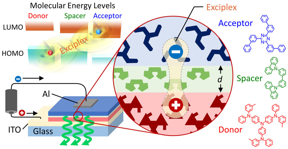
By manipulating the molecular distance between the electron-donating molecule (donor) and the electron-accepting molecule (acceptor) that carry the exciplex’s hole and electron, respectively, the researchers could modify the properties of these weakly bound excitons.
basic structure of an exciplex-based OLED with emission color and efficiency that can be controlled simply by changing the spacer thickness
This schematic shows the basic structure of an exciplex-based OLED with emission color and efficiency that can be controlled simply by changing the spacer thickness. An exciplex forms when a hole in the highest occupied molecular orbital (HOMO) of a donor molecule is attracted to an electron in the lowest unoccupied molecular orbital (LUMO) of an acceptor molecule. Light is emitted when the electron releases energy as light and transfers across the spacer layer to the donor molecule, thus replacing the missing electron represented by the hole. The thickness of the spacer can be used to modify the attraction between the hole and electron and tune the exciplex energy. Without changing any of the molecules, emission color could be varied from orange to yellowish green and the efficiency enhanced eight fold by increasing the spacer thickness to 5 nm. (click on image to enlarge)
„What we did is similar to placing sheets of paper between a magnet and a refrigerator,” said Associate Professor Hajime Nakanotani, lead author of the paper reporting these results published online February 26, 2016, in the journal Science Advances („Long-range coupling of electron-hole pairs in spatially separated organic donor-acceptor layers”).
„By increasing the thickness of an extremely thin layer of organic molecules inserted as a spacer between the donor and acceptor, we could reduce the attraction between the hole and electron in the exciplex and thereby greatly influence the exciplex’s energy, lifetime, and emission color and efficiency.”
Indeed, the changes can be large: by inserting a spacer layer with a thickness of only 5 nm between a donor layer and an acceptor layer in an OLED, the emission color shifted from orange to yellowish green and the light emission efficiency increased 700%.
For this to work, the organic molecule used for the spacer layer must have an excitation energy higher than those of the donor and acceptor, but such materials are already widely available.
While the molecular distance is currently determined by the thickness of the vacuum-deposited spacer layer, the researchers are now looking into other ways to control the distance.
„This gives us a powerful way to greatly vary device properties without redesigning or changing any of the materials,” said Professor Chihaya Adachi, director of OPERA. „In the future, we envision new types of exciton-based devices that respond to external forces like pressure to control the distance and electrical behavior.”
In addition, the researchers found that the exciplexes were still formed when the spacer was 10 nm thick, which is long on a molecular scale.
„This is some of the first evidence that electrons and holes could still interact like this across such a long distance,” commented Professor Adachi, „so this structure may also be a useful tool for studying and understanding the physics of excitons to design better OLEDs and organic solar cells in the future.”
„From both scientific and applications standpoints, we are excited to see where this new path for exciton engineering takes us and hope to establish a new category of exciton-based electronics.”
Source: Kyushu University

Read more: Artificial control of exciplexes opens possibilities for new electronics

Cum cresc grupurile metalice

Procesele de transformare a clusterelor metalice au loc rapid. În mod normal, nu este posibil să se respecte aceste procese și produsele intermediare. „Chiar și primii pași sunt în mare parte necunoscuți și pot fi identificați numai prin combinarea sintezei cu măsurarea și modelarea chimică computerizată”, spun experții. Dacă s-ar cunoaște toate etapele de dezvoltare, grupurile metalice cu proprietăți optoelectronice și magnetice ajustate fin pot fi personalizate pentru aplicații tehnice.
În studiul publicat acum, echipa raportează formarea unui cluster metalic multinucleat, prin sintetizarea mai întâi a unei serii de clustere cu dimensiuni variabile ale metaloizilor germaniu și arsenic. Clusterele mai mari au un atom de tantal de metal tranzițional în centrul moleculelor de colivie. Măsurătorile și simulările pe calculator sugerează că metalul de tranziție joacă foarte devreme un rol în formarea clusterelor.

Posted: Feb 26, 2016

How metal clusters grow

(Nanowerk News) First the nucleus, then the shell: Researchers from Marburg and Karlsruhe have studied stepwise formation of metal clusters, smallest fractions of metals in molecular form. The shell gradually forms around the inner atom rather than by later inclusion of the central atom. Knowledge of all development steps may allow for customized optoelectronic and magnetic properties, as is reported by the researchers in the science journal Nature Communications („Understanding of multimetallic cluster growth”).

formation of a metal cluster from the atomic constituents to the compound
Step by step towards the complete shell: formation of a metal cluster from the atomic constituents to the compound. (Image: Dehnen Group, Philipps-Universität Marburg) (click on image to enlarge)
To specifically synthesize chemical compounds, mechanisms responsible for their formation have to be known. „Purely inorganic compounds are a black box in this respect,” Florian Weigend of Karlsruhe Institute of Technology (KIT) and Stefanie Dehnen of Philipps-Universität Marburg, the corresponding authors of this study, explain. „This particularly applies to the formation of multinucleated metal complexes, so-called clusters.”
Processes of transforming metal clusters take place rapidly. Normally, it is not possible to observe these processes and the intermediate products. „Even the very first steps are largely unknown and can only be identified by combining synthesis with measurement and computerized chemical modeling,” the experts say. If all development steps were known, metal clusters with finely adjusted optoelectronic and magnetic properties might be customized for technical applications.
In the study published now, the team reports the formation of a multinucleated metal cluster by first synthesizing a series of variably sized clusters of the metalloids germanium and arsenic. Larger clusters have an atom of the transition metal tantalum in the center of the cage molecules. Measurements and computer simulations suggest that the transition metal very early plays a role in cluster formation.
„It may be considered a type of catalyst that initiates the formation and breaking of bonds,” Weigend and Dehnen point out. Altogether, the findings show that the transition metal does not settle into an earlier formed cluster shell, but that the shell of the cluster gradually forms around the atom in the center. „The results can be generalized for a whole family of metallic cluster compounds,” Weigend and Dehnen say.
Apart from chemical syntheses and measurements in Marburg, extensive computer simulations with the largely KIT-developed quantum chemistry program package TURBOMOLE were made at KIT. In this way, the role of the many isomers in the reaction was determined. Isomers are chemical compounds of identical composition, but with different spatial arrangements of the atoms.
„Thanks to the calculation of reaction paths, we have found that transformations of isomers are possible with a relatively small energy expenditure,” Weigend says.
Source: Karlsruhe Institute of Technology

Read more: How metal clusters grow

Inginerii descoperă un nou tip de material semiconductor 2D pentru electronică(Engineers discover a new kind of 2D semiconducting material for electronics)

Inginerii de la Universitatea din Utah au descoperit un nou tip de material semiconductor 2D pentru electronică, care deschide ușa pentru computerele mult mai rapide și smartphone-urile care consumă și mai puțină putere.
Semiconductorul, realizat din elemente de staniu și oxigen sau monoxid de staniu (SnO), este un strat de material 2D cu un singur atom gros, permițând încărcăturilor electrice să se deplaseze mult mai repede decât materialele convenționale 3D, cum ar fi siliciul. Acest material ar putea fi folosit în tranzistori, sângele vieții tuturor dispozitivelor electronice, cum ar fi procesoarele de calculator și procesoarele grafice în computerele desktop și dispozitivele mobile

Posted: Feb 15, 2016

Engineers discover a new kind of 2D semiconducting material for electronics

(Nanowerk News) University of Utah engineers have discovered a new kind of 2D semiconducting material for electronics that opens the door for much speedier computers and smartphones that also consume a lot less power.

The semiconductor, made of the elements tin and oxygen, or tin monoxide (SnO), is a layer of 2D material only one atom thick, allowing electrical charges to move through it much faster than conventional 3D materials such as silicon. This material could be used in transistors, the lifeblood of all electronic devices such as computer processors and graphics processors in desktop computers and mobile devices. The material was discovered by a team led by University of Utah materials science and engineering associate professor Ashutosh Tiwari.
Ashutosh Tiwari, University of Utah
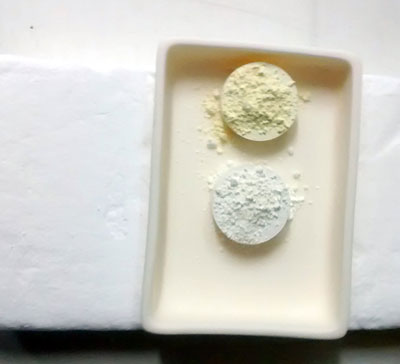
University of Utah materials science and engineering associate professor Ashutosh Tiwari holds up a substrate layered with a newly discovered 2-D material made of tin and oxygen. Tiwari and his team have discovered this new material, tin monoxide, which allows electrical charges to move through it much faster than common 3-D material such as silicon. This breakthrough in semiconductor material could lead to much faster computers and mobile devices such as smartphones that also run on less power and with less heat. (Photo: Dan Hixson/University of Utah College of Engineering)
A paper describing the research was published online Monday, Feb. 15, 2016 in the journal, Advanced Electronic Materials („2D Tin Monoxide—An Unexplored p-Type van der Waals Semiconductor: Material Characteristics and Field Effect Transistors”). The paper, which also will be the cover story on the printed version of the journal, was co-authored by University of Utah materials science and engineering doctoral students K. J. Saji and Kun Tian, and Michael Snure of the Wright-Patterson Air Force Research Lab near Dayton, Ohio.
Transistors and other components used in electronic devices are currently made of 3D materials such as silicon and consist of multiple layers on a glass substrate. But the downside to 3D materials is that electrons bounce around inside the layers in all directions.
The benefit of 2D materials, which is an exciting new research field that has opened up only about five years ago, is that the material is made of one layer the thickness of just one or two atoms. Consequently, the electrons „can only move in one layer so it’s much faster,” says Tiwari.
While researchers in this field have recently discovered new types of 2D material such as graphene, molybdenun disulfide and borophene, they have been materials that only allow the movement of N-type, or negative, electrons. In order to create an electronic device, however, you need semiconductor material that allows the movement of both negative electrons and positive charges known as „holes.” The tin monoxide material discovered by Tiwari and his team is the first stable P-type 2D semiconductor material ever in existence.
„Now we have everything – we have P-type 2D semiconductors and N-type 2D semiconductors,” he says. „Now things will move forward much more quickly.”
Now that Tiwari and his team have discovered this new 2D material, it can lead to the manufacturing of transistors that are even smaller and faster than those in use today. A computer processor is comprised of billions of transistors, and the more transistors packed into a single chip, the more powerful the processor can become.
Transistors made with Tiwari’s semiconducting material could lead to computers and smartphones that are more than 100 times faster than regular devices. And because the electrons move through one layer instead of bouncing around in a 3D material, there will be less friction, meaning the processors will not get as hot as normal computer chips. They also will require much less power to run, a boon for mobile electronics that have to run on battery power. Tiwari says this could be especially important for medical devices such as electronic implants that will run longer on a single battery charge.
„The field is very hot right now, and people are very interested in it,” Tiwari says. „So in two or three years we should see at least some prototype device.”
Source: University of Utah