New solar-powered organic compound to tackle air and water pollution(Compus organic bazat pe energie solară pentru combaterea poluării aerului și a apei)

Este ieftin să producă și deloc toxice, dioxidul de titan (cunoscut ca titania) are multe utilizări. Este folosit ca un pigment pentru a asigura albitatea și opacitatea pentru totul, de la săpunuri, cosmetice, vopsele, hârtie la alimente, pastă de dinți și medicamente. Este, de asemenea, utilizat pe scară largă ca o protecție solară, datorită capacităților puternice de absorbție a luminii UV.
Este, de asemenea, un fotocatalizator excelent, reacționând sub lumină ultravioletă pentru a deveni un agent de sterilizare. Totuși, deoarece lumina UV reprezintă doar 5% din radiația solară, titanele albe sunt relativ ineficiente în acest rol.
În acest studiu, cercetătorii au adăugat un compus obișnuit prezent în coloranții de păr în timpul preparării dioxidului de titan pentru a crea „titania neagră”. Deoarece negrul absoarbe o gamă mult mai largă a spectrului solar, titanul negru prezintă o activitate fotocatalitică mult mai eficientă atât în ​​domeniul luminii UV, cât și al luminii vizibile.
Ca atare, titanii negri găsesc utilizări semnificative în instalațiile de tratare a apei și cum ar fi curățarea bazinelor. Acționat numai de lumina soarelui, este capabil să descompună poluanții organici și să purifice apa.
Se poate aplica și pe drumurile, fațadele și terasele clădirilor, unde acest „praf negru”funcționează pentru a elimina oxidul de azot din atmosferă și a îmbunătăți calitatea aerului.a modificat culoarea dioxidului de titan de la alb la negru pentru a fi utilizat ca agent eficient de sterilizare, eliminând contaminanții organici din aer și apă.

Posted: Feb 12, 2016

New solar-powered organic compound to tackle air and water pollution

(Nanowerk News) Nanoscientists at the Univeristy of Alicante have modified a commonly-used compound, titanium dioxide, turning it from white to black to boost its efficiency and make environmental applications a real possibility.

Researcher Elena Serrano at the Universidad de Alicante (University of Alicante, UA) has modified the colour of titanium dioxide from white to black for use as an efficient sterilising agent, removing organic contaminants from air and water.
Black and white titania
Black and white titanias. (Image: NANOMOL, University of Alicante)
Cheap to produce and not at all toxic, titanium dioxide (known as titania) has many uses. It is used as a pigment to provide whiteness and opacity to everything from soaps, cosmetics, paints, paper to foods, toothpaste and medicines. It is also widely used as a sunscreen, due to its strong UV light-absorbing capabilities.
It is also an excellent photocatalyst, reacting under ultraviolet light to become a sterilising agent. However, since UV light accounts for just 5% of solar radiation, white titania is relatively inefficient in this role.
In this study, researchers added a common compound present in hair dyes during the preparation of the titanium dioxide to create “black titania”. Since black absorbs a much larger range of the solar spectrum, black titania presents a much more efficient photocatalytic activity in both the UV and visible light ranges.
As such, black titania finds significant uses in water treatment plants and such as pool cleaning. Powered only by sunlight, it is able to break down organic pollutants and purify the water.
It can also be applied to roads, building facades and terraces, where this “black dust” works to remove nitrogen oxide from the atmosphere and improve air quality.
Although similar technologies do already exist, “they generally require the use of noble metals like gold, or are the result of very complicated synthesis procedures, both of which are very expensive. Our black titania is much more efficient and cost-effective to produce, needing only water, alcohol and mild temperatures” (Serrano).
The simple and cost-effective new procedure has been patented by the UA under the title (translated) “Procedure for the in-situ synthesis of functionalised titanias and their uses”. Elena Serrano appears as co-author, alongside the director of the UV’s Molecular Nanotechnology Lab (NANOMOL), Javier García, where the work has been carried out.
Source: Univeristy of Alicante

Read more: New solar-powered organic compound to tackle air and water pollution

Grafen se sprijină pe sticlă pentru a avansa electronica (Graphene leans on glass to advance electronics )

a crea grafenă flexibilă, personalizată și cu performanțe ridicate: stratificându-l pe partea de sus a sticlei comune. Acest proces scalabil și ieftin facilitează deschiderea unei noi clase de dispozitive microelectronice și optoelectronice – totul de la celule solare eficiente la ecrane tactile.De exemplu, conductivitatea ridicată și transparența graphenei o fac un candidat foarte promițător ca un electrod transparent și conducător pentru a înlocui oxidul de staniu indiu relativ fragil și scump (ITO) în aplicații cum ar fi celule solare, diode emițătoare de lumină organică (OLED) afișaje și ecrane tactile. Pentru a înlocui ITO, trebuie dezvoltate metode scalabile și cu costuri scăzute pentru a controla rezistența grafenului la fluxul de curent electric prin controlarea puterii de dopaj. Acest nou sistem de sticla-grafen se poate ridica la aceasta provocare, spun cercetatorii.

Posted: Feb 12, 2016

Graphene leans on glass to advance electronics

(Nanowerk News) Graphene, the two-dimensional powerhouse, packs extreme durability, electrical conductivity, and transparency into a one-atom-thick sheet of carbon. Despite being heralded as a breakthrough „wonder material,” graphene has been slow to leap into commercial and industrial products and processes.

Now, scientists have developed a simple and powerful method for creating resilient, customized, and high-performing graphene: layering it on top of common glass. This scalable and inexpensive process helps pave the way for a new class of microelectronic and optoelectronic devices—everything from efficient solar cells to touch screens.
The collaboration—led by scientists at the U.S. Department of Energy’s (DOE) Brookhaven National Laboratory, Stony Brook University (SBU), and the Colleges of Nanoscale Science and Engineering at SUNY Polytechnic Institute—published their results February 12, 2016, in the journal Scientific Reports („Spontaneous and strong multi-layer graphene n-doping on soda-lime glass and its application in graphene-semiconductor junctions”).
Schematic of a graphene field-effect-transistor
Left: Schematic of a graphene field-effect-transistor used in this study. The device consists of a solar cell containing graphene stacked on top of a high-performance copper indium gallium diselenide (CIGS) semiconductor, which in turn is stacked on an industrial substrate (either soda-lime glass, SLG, or sodium-free borosilicate glass, BSG). The research revealed that the SLG substrate serves as a source of sodium doping, and improved device performance in a way not seen in the sodium-free substrate. Right: A scanning electron micrograph of the device as seen from above, with the white scale bar measuring 10 microns, and a transmission electron micrograph inset of the CIGS/graphene interface where the white scale bar measures 100 nanometers. (click on image to enlarge)
„We believe that this work could significantly advance the development of truly scalable graphene technologies,” said study coauthor Matthew Eisaman, a physicist at Brookhaven Lab and professor at SBU.
The scientists built the proof-of-concept graphene devices on substrates made of soda-lime glass—the most common glass found in windows, bottles, and many other products. In an unexpected twist, the sodium atoms in the glass had a powerful effect on the electronic properties of the graphene.
„The sodium inside the soda-lime glass creates high electron density in the graphene, which is essential to many processes and has been challenging to achieve,” said coauthor Nanditha Dissanayake of Voxtel, Inc., but formerly of Brookhaven Lab. „We actually discovered this efficient and robust solution during the pursuit of something a bit more complex. Such surprises are part of the beauty of science.”
Crucially, the effect remained strong even when the devices were exposed to air for several weeks—a clear improvement over competing techniques.
The experimental work was done primarily at Brookhaven’s Sustainable Energy Technologies Department and the Center for Functional Nanomaterials (CFN), which is a DOE Office of Science User Facility.
The graphene tweaks in question revolve around a process called doping, where the electronic properties are optimized for use in devices. This adjustment involves increasing either the number of electrons or the electron-free „holes” in a material to strike the perfect balance for different applications. For successful real-world devices, it is also very important that the local number of electrons transferred to the graphene does not degrade over time.
„The graphene doping process typically involves the introduction of external chemicals, which not only increases complexity, but it can also make the material more vulnerable to degradation,” Eisaman said. „Fortunately, we found a shortcut that overcame those obstacles.”
The team initially set out to optimize a solar cell containing graphene stacked on a high-performance copper indium gallium diselenide (CIGS) semiconductor, which in turn was stacked on an industrial soda-lime glass substrate.
The scientists then conducted preliminary tests of the novel system to provide a baseline for testing the effects of subsequent doping. But these tests exposed something strange: the graphene was already optimally doped without the introduction of any additional chemicals.
„To our surprise, the graphene and CIGS layers already formed a good solar cell junction!” Dissanayake said. „After much investigation, and the later isolation of graphene on the glass, we discovered that the sodium in the substrate automatically created high electron density within our multi-layered graphene.”
Pinpointing the mechanism by which sodium acts as a dopant involved a painstaking exploration of the system and its performance under different conditions, including making devices and measuring the doping strength on a wide range of substrates, both with and without sodium.
„Developing and characterizing the devices required complex nanofabrication, delicate transfer of the atomically thin graphene onto rough substrates, detailed structural and electro-optical characterization, and also the ability to grow the CIGS semiconductor,” Dissanayake said. „Fortunately, we had both the expertise and state-of-the-art instrumentation on hand to meet all those challenges, as well as generous funding.”
The bulk of the experimental work was conducted at Brookhaven Lab using techniques developed in-house, including advanced lithography. For the high-resolution electron microscopy measurements, CFN staff scientists and study coauthors Kim Kisslinger and Lihua Zhang lent their expertise. Coauthors Harry Efstathiadis and Daniel Dwyer—both at the College of Nanoscale Science and Engineering at SUNY Polytechnic Institute—led the effort to grow and characterize the high-quality CIGS films.
„Now that we have demonstrated the basic concept, we want to focus next on demonstrating fine control over the doping strength and spatial patterning,” Eisaman said.
The scientists now need to probe more deeply into the fundamentals of the doping mechanism and more carefully study material’s resilience during exposure to real-world operating conditions. The initial results, however, suggest that the glass-graphene method is much more resistant to degradation than many other doping techniques.
„The potential applications for graphene touch many parts of everyone’s daily life, from consumer electronics to energy technologies,” Eisaman said. „It’s too early to tell exactly what impact our results will have, but this is an important step toward possibly making some of these applications truly affordable and scalable.”
For example, graphene’s high conductivity and transparency make it a very promising candidate as a transparent, conductive electrode to replace the relatively brittle and expensive indium tin oxide (ITO) in applications such as solar cells, organic light emitting diodes (OLEDs), flat panel displays, and touch screens. In order to replace ITO, scalable and low-cost methods must be developed to control graphene’s resistance to the flow of electrical current by controlling the doping strength. This new glass-graphene system could rise to that challenge, the researchers say.
Source: Brookhaven National Laboratory

Read more: Graphene leans on glass to advance electronics

O bază mai bună pentru memoria 3D

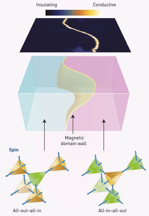
Kentaro Ueda de la Centrul RIKEN pentru Știința Emergent Matter și colegii săi au investigat pyrochlore de iodură de neodim (Nd 2 Ir 2 O 7 ), un izolator magnetic cu pământuri rare, cu proprietăți neobișnuite. Spinurile din acest material sunt aranjate tetraedral și alternativ îndreptate „all-in” spre centrul tetraedrului, sau în fața „all-out”. Doua tipuri de domenii magnetice se formeaza in Nd 2 Ir 2 O 7 – ” totul in tot” sau „totul out-all-in” (fig.1) – si unele studii la scara larga au sugerat o conductivitate anormala Care se petrec la barierele dintre ele.

Posted: Feb 05, 2016

A better foundation for 3D memory

(Nanowerk News) Efforts to shrink memory devices beyond the limits imposed by conventional lithography have focused on nanoscale regions, known as magnetic domain walls, which can be manipulated in three dimensions. Now, RIKEN researchers and international collaborators have detected a new type of domain wall with highly conductive, mobile metallic states that promises to make three-dimensional memory systems easier to control and miniaturize (Science, „Mobile metallic domain walls in an all-in-all-out magnetic insulator”).

metal-like domain walls emerge at the nanoscale when two insulating, ‘all-in–all-out’ magnetic phases come into contact
Scanning probe experiments reveal that metal-like domain walls emerge at the nanoscale when two insulating, ‘all-in–all-out’ magnetic phases come into contact. (Image: Eric Yue Ma, Stanford University)
Magnetic materials contain distinct regions, known as domains, in which electrons with the same spin configuration—normally spin-up or spin-down states—are separated by domain wall boundaries. Recent theoretical studies have suggested that domain walls adopt different electronic states and become electrically active in certain magnetic insulators. But detecting metallic behavior in insulating crystals, where grains are often smaller than the width of a human hair, is experimentally challenging.
Kentaro Ueda from the RIKEN Center for Emergent Matter Science and colleagues investigated neodymium iridate pyrochlore (Nd2Ir2O7), a rare-earth-based magnetic insulator with unusual properties. Spins in this material are arranged tetrahedrally and alternately point ‘all-in’ toward the center of the tetrahedron, or face ‘all-out’. Two types of magnetic domains form in Nd2Ir2O7—‘all-in–all-out’ or ‘all-out–all-in’ (Fig. 1)—and some large-scale studies have hinted at abnormal conductivity occurring at the barriers between them.
The team used a technique called microwave impedance microscopy to obtain direct nanoscale information on the domain walls of Nd2Ir2O7. Samples were cooled to close to absolute zero and their surfaces were then scanned by an ultrasharp and highly conductive probe that senses variations in electrical resistance. The resulting images revealed the presence of narrow, curvilinear features, roughly 100 nanometers wide, that were hundreds of times more conductive than surrounding regions.
“The emergence of metallic domain walls, in spite of the fully insulating bulk state, provoked a lot of discussion in our team,” says Ueda. “Where does this behavior originate? And why is this material so special?”
The strong response of the nanoscale regions to thermal and magnetic fields provided some clues to these questions. “In conventional metals, resistivity usually depends on temperature,” explains Ueda. “The domain walls show virtually temperature-independent ohmic behavior, indicating an anomalous metallic defect or edge state.”
One potential application of this technology is magnetic random access memory (MRAM), in which data is stored by altering the electrical resistance of the recording medium. Currently, resistance changes of several tens of per cent are used in MRAM. In contrast, metallic domains can change the resistance by factors of several hundred, which should enable much more compact MRAM devices to be fabricated.
Source: RIKEN

Read more: A better foundation for 3D memory

Nanomaterialul unei noi clase

Cercetătorii de cercetare au dezvoltat o nouă tehnică care produce un material care este în același timp puternic, dur și rigid. Pentru a realiza acest lucru, oamenii de știință au folosit mai întâi o procedură standard, folosită pe scară largă atunci când lucrează cu nanoparticule, prin care nanoparticulele din ceramică de fier sunt depozitate într-o gamă regulată. Acest lucru se face cu ajutorul acidului oleic organic, care intră în golul îngust între nanoparticule și le ține împreună

Posted: Feb 05, 2016

Nanomaterial of a new class

(Nanowerk News) Classical materials such as ceramics, metals and polymers have their typical mechanical properties. They are hard, soft, strong, flexible or stiff. Hamburg research scientists have now synthesized a material that unites several different properties, and could thereby open the way to new applications in medical engineering and manufacturing. The scientists from the Hamburg University of Technology (TUHH), the University of Hamburg, the Helmholtz Centre Geesthacht and DESY have presented their novel nanocomposite in the journal Nature Materials („Organically linked iron oxide nanoparticle supercrystals with exceptional isotropic mechanical properties”).

Ultra-high vacuum chamber at the DESY-NanoLab
Ultra-high vacuum chamber at the DESY-NanoLab, in which the spectroscopic analysis was carried out to characterise the nature of the bond formed by the oleic acid molecules. (Image: DESY)
This new class of material could for example be suitable for filling dental cavities, or manufacturing watch cases. The materials used in applications like these need to be both hard and damage-tolerant.
The research scientists have developed a new technique which produces a material that is at the same time strong, hard and stiff. To achieve this, the scientists first employed a standard procedure, widely used when working with nanoparticles, whereby ceramic iron oxide nanoparticles are deposited in a regular array. This is done with the help of organic oleic acid, which seeps into the narrow gaps between the nanoparticles and holds them together.
“The self-organisation of these nanoparticles leads to an extended, closely packed supercrystal reminiscent of atomic crystal lattices,” explains one of the authors, Axel Dreyer from the TUHH.
The crucial discovery is that by subsequently exposing the material to moderate heat levels, the resulting nanocomposite displays a much stronger cohesion and its mechanical properties are unlike those of any other.
transmission electron microscope image of  iron oxide nanoparticles, immersed in oleic acid
High resolution transmission electron microscope image of the iron oxide nanoparticles, immersed in oleic acid. (Image: TUHH)
On the smallest scale, the structure of the new material resembles that of biological hard tissues, such as mother of pearl and dental enamel. It consists of uniformly sized iron oxide nanoparticles, which are coated with oleic acid. In previous studies, the bonds between the oleic acid molecules were very weak and due to so-called Van der Waals’ forces. By drying and pressing the material at an elevated temperature and then applying a controlled thermal treatment, the scientist have now managed to create a much stronger bond between the oleic acid molecules, thereby markedly improving the mechanical properties of the nanocomposite.
Since oleic acid is very often used when processing other nanoparticles too, this new method could potentially improve the mechanical properties of a great many other nanocomposites as well. The bonding properties of the oleic acid, which serves as an adhesive, have been examined spectroscopically by the staff of the DESY-Nanolab. “Our measurements showed that the oleic acid molecules survive the thermal treatment and form additional crosslinks during the process,” reports co-author Andreas Stierle, a Leading Scientist at DESY. “This important finding can serve as the basis for successfully modelling the mechanical properties of this novel material.”
Source: Deutsches Elektronen-Synchrotron

Read more: Nanomaterial of a new class

Oțeluri cu oxid de metal: O nouă opțiune de manipulare a proprietăților interfețelor

Am reușit să combinăm doi oxizi de metal de tranziție foarte diferiți: în timp ce în electronii titanați, legăturile chimice sunt puternic localizate în jurul ionilor, în partea de nickelat acești electroni sunt împărțiți între ionii de nichel și oxigen și, prin urmare, foarte covalent „, Explică Manuel Bibes.
Când se pun împreună ambele materiale, o anumită încărcare se transferă de la stratul de titanat la cel de aluminiu. Ei au investigat acest proces de transfer de sarcină pentru eșantioane care conțin diferite elemente de pământuri rare în stratul de nichelat, cum ar fi Lanthanum, Neodymium și Samarium la BESSY II.

Posted: Feb 04, 2016

Metal oxide sandwiches: New option to manipulate properties of interfaces

(Nanowerk News) Sandwich systems of thin film transition metal oxides display surprising properties at their interfaces. In case of the paradigmatic example of Lanthan-Aluminate ( LaAlO3) and Strontium-Titanate (SrTiO3) both materials are insulators and non-magnetic, while their interface has been observed to display ferromagnetism, high electrical conductivity and even superconductivity.

Now the team of Manuel Bibes, CNRS Thales at Palaiseau, France, in collaboration with scientists at HZB around Sergio Valencia and several European groups, devised a new approach to tailor interface properties. Together they designed a series of experiments at the synchrotron source BESSY II to shed more light on the emergence of such property changes, identifying a new „knob” for their control (Nature Physics, „Hybridization-controlled charge transfer and induced magnetism at correlated oxide interfaces”).
metal oxide layers
This is a sketch of the structure of both metal oxide layers. Interesting new properties can arise at the interface. (Image: M. Bibes)
Rare-Earth Elements influence charge transfer
The samples, which the team of Manuel Bibes did produce, consisted of a sandwich of 2 nm Gadolinium-Titanate (GdTiO3) and „R”-Nickelate (RNiO3) films, where R is a rare-earth element. „We have been able to combine two very different transition metal oxides: whereas in the titanate electrons in the chemical bonds are strongly localized around the ions, in the nickelate side these electrons are shared between Nickel- and Oxygen-ions, and thus highly covalent”, Manuel Bibes explains.
When putting both materials together some charge is transferred from the titanate layer to the nickelate one. They investigated this charge transfer process for samples containing different rare-earth elements in the nickelate layer such as Lanthanum, Neodymium and Samarium at BESSY II.
Their results show that the charge transfer at the interface between the materials strongly depends on the rare earth element in the nickelate layer. Different rare-earth elements have different atomic radii (size).This modifies the interaction between the Ni and O atoms and the degree of „covalency” between Ni and O changes. This was already known, but now the scientists have observed that this also affects the charge transferred from the GdTiO3 to the Nickelate film. „This is the key result”, Sergio Valencia from HZB explains. „We have found a new „knob”. Covalency (which is controlled by changing R) controls the charge transfer between the titanate and the nickelate.”
Ferromagnetism observed, superconductivity still searched
Tuning the charge transfer in this way might allow to control the formation of new interfacial phases too. For example, the scientists observed a new ferromagnetic phase at the interface. „Our work may help in the ongoing quest for cuprate-like superconductivity in nickelate heterostructures”, Valencia says. „We hope that this study will help to design better interfaces for exploring new exciting new phases of matter at interfaces between covalent materials”, Bibes adds.
Source: Helmholtz-Zentrum Berlin für Materialien und Energie

Read more: Metal oxide sandwiches: New option to manipulate properties of interfaces

Cercetătorii caută mijloace eficiente de împărțire a apei cu nanoroduri

Hidrogenul din aceste reacții ar putea alimenta vehicule cu pile de combustie cu hidrogen curate sau ar putea fi combinat cu dioxid de carbon pentru a produce metanol, care ar putea fi distribuit prin sistemul nostru existent de combustibil lichid. Această din urmă abordare are avantajul suplimentar de a scoate dioxidul de carbon din atmosferă.

Posted: Feb 04, 2016

Researchers seek efficient means of splitting water with nanorods

(Nanowerk News) Photovoltaics promise to help meet our energy needs by turning sunlight into electricity. We can’t run everything that way, but with a little tweaking, photovoltaic materials can use solar energy to split water into hydrogen and oxygen.

Cornell researchers are studying how this works, hoping to make the process more efficient and less expensive. “There are several existing systems, but none actually work well,” said Peng Chen, the Peter J. W. Debye Professor of Chemistry.
Hydrogen from these reactions could power vehicles with clean-burning hydrogen fuel cells, or could be combined with carbon dioxide to make methanol, which could be distributed through our existing liquid-fuel system. The latter approach has the added benefit of taking carbon dioxide out of the atmosphere.
Chen and colleagues studied water-splitting activity on the surface of nanorods of the semiconductor titanium dioxide, finding that variations in the structure of the surface determine where and how the reaction takes place. They report their results in the Feb. 4 issue of the journal Nature („Sub-particle reaction and photocurrent mapping to optimize catalyst-modified photoanodes”).
Flashes of fluorescence seen under a microscope
Flashes of fluorescence seen under a microscope show where chemical reactions to (b) split water molecules or (c) electric currents take place on a nanorod of photovoltaic material. The outline of the rod laid over flash images is taken from the scanning electron microscope image at right.
When a photon of light hits a crystal of titanium dioxide, the added energy kicks an electron into a higher energy level, leaving behind a “hole” – a space where an electron ought to be but isn’t, that looks like a positive charge. If electrodes are attached to the crystal, the free electrons will flow through a circuit as an electric current.
But in the presence of a catalyst – in this case cobalt borate – the array of positive charges can withdraw electrons from a water molecule (whose formula can be written as H-O-H), pulling it apart into a positively charged proton – the nucleus of a hydrogen atom – and a neutral hydroxyl radical, or OH. The OH radicals combine into hydrogen peroxide (H-O-O-H), which the catalytic reaction again pulls apart into protons and oxygen.
To study the reaction, Chen’s research team focused a powerful microscope on titanium dioxide rods about 127×1,735 nanometers in a microfluidic chamber through which water was flowed. A light microscope can’t see chemical reactions, so Chen employed a technique he calls “fluorescence microscopy,” adding chemicals to the water that change into a fluorescent material when the reactions take place. One changes in the presence of free electrons; the other changes in the presence of OH radicals, which are produced when water is split. When the sample is zapped with a laser to induce fluorescence, the microscope sees flashes of light that reveal where the reactions are taking place.
Alternating from one probe to the other, they observed that the reactions were not distributed evenly across the surface. Water splitting occurred only at certain “hotspots” that seem to be characterized by some irregularities in the surface or the presence of a few “doping” atoms.
“This gives us a way to improve the process,” Chen said. “Now we know where to deposit the catalyst according to the map of the hole and electron reactions on each nanorod.”
The researchers propose a method for selectively depositing catalyst on the areas that will be most productive.
Source:By Bill Steele, Cornell University

Read more: Researchers seek efficient means of splitting water with nanorods

Oamenii de știință îndrume nanoparticulele de aur pentru a forma supralaturi „diamante”

poate deschide o cale către noi materiale care să profite de proprietățile optice și mecanice ale acestei Structura cristalină pentru aplicații precum tranzistoare optice, materiale de schimbare a culorii și materiale ușoare, dar dure.

Posted: Feb 04, 2016

Scientists guide gold nanoparticles to form ‘diamond’ superlattices

(Nanowerk News) Using bundled strands of DNA to build Tinkertoy-like tetrahedral cages, scientists at the U.S. Department of Energy’s Brookhaven National Laboratory have devised a way to trap and arrange nanoparticles in a way that mimics the crystalline structure of diamond. The achievement of this complex yet elegant arrangement, as described in a paper published February 5, 2016, in Science („Diamond family of nanoparticle superlattices”), may open a path to new materials that take advantage of the optical and mechanical properties of this crystalline structure for applications such as optical transistors, color-changing materials, and lightweight yet tough materials.

„We solved a 25-year challenge in building diamond lattices in a rational way via self-assembly,” said Oleg Gang, a physicist who led this research at the Center for Functional Nanomaterials (CFN, www.bnl.gov/cfn/) at Brookhaven Lab in collaboration with scientists from Stony Brook University, Wesleyan University, and Nagoya University in Japan.
guiding gold nanoparticles to form 'diamond' superlattices
Schematic illustration of the experimental strategy: Double stranded DNA bundles (gray) form tetrahedral cages. Single stranded DNA strands on the edges (green) and vertices (red) match up with complementary strands on gold nanoparticles. This results in a single gold particle being trapped inside each tetrahedral cage, and the cages binding together by tethered gold nanoparticles at each vertex. The result is a crystalline nanoparticle lattice that mimics the long-range order of crystalline diamond. The images below the schematic are (left to right): a reconstructed cryo-EM density map of the tetrahedron, a caged particle shown in a negative-staining TEM image, and a diamond superlattice shown at high magnification with cryo-STEM. (click on image to enlarge)
The scientists employed a technique developed by Gang that uses fabricated DNA as a building material to organize nanoparticles into 3D spatial arrangements [ www.bnl.gov/newsroom/news.php?a=11728]. They used ropelike bundles of double-helix DNA to create rigid, three-dimensional frames, and added dangling bits of single-stranded DNA to bind particles coated with complementary DNA strands.
„We’re using precisely shaped DNA constructs made as a scaffold and single-stranded DNA tethers as a programmable glue that matches up particles according to the pairing mechanism of the genetic code-A binds with T, G binds with C,” said Wenyan Liu of the CFN, the lead author on the paper. „These molecular constructs are building blocks for creating crystalline lattices made of nanoparticles.”
The difficulty of diamond
As Liu explained, „Building diamond superlattices from nano- and micro-scale particles by means of self-assembly has proven remarkably difficult. It challenges our ability to manipulate matter on small scales.”
The reasons for this difficulty include structural features such as a low packing fraction-meaning that in a diamond lattice, in contrast to many other crystalline structures, particles occupy only a small part of the lattice volume-and strong sensitivity to the way bonds between particles are oriented. „Everything must fit together in just such a way without any shift or rotation of the particles’ positions,” Gang said. „Since the diamond structure is very open, many things can go wrong, leading to disorder.”
„Even to build such structures one-by-one would be challenging,” Liu added, „and we needed to do so by self-assembly because there is no way to manipulate billions of nanoparticles one-by-one.”
Gang’s previous success using DNA to construct a wide range of nanoparticle arrays suggested that a DNA-based approach might work in this instance.
DNA guides assembly
The team first used the ropelike DNA bundles to build tetrahedral „cages”-a 3D object with four triangular faces. They added single-stranded DNA tethers pointing toward the interior of the cages using T,G,C,A sequences that matched up with complementary tethers attached to gold nanoparticles. When mixed in solution, the complementary tethers paired up to „trap” one gold nanoparticle inside each tetrahedron cage.
The arrangement of gold nanoparticles outside the cages was guided by a different set of DNA tethers attached at the vertices of the tetrahedrons. Each set of vertices bound with complementary DNA tethers attached to a second set of gold nanoparticles.
When mixed and annealed, the tetrahedral arrays formed superlattices with long-range order where the positions of the gold nanoparticles mimics the arrangement of carbon atoms in a lattice of diamond, but at a scale about 100 times larger.
Brookhaven Lab’s Oleg Gang describes the idea of using DNA to drive the self-assembly of materials from nanoscale particles.
„Although this assembly scenario might seem hopelessly unconstrained, we demonstrate experimentally that our approach leads to the desired diamond lattice, drastically streamlining the assembly of such a complex structure,” Gang said.
The proof is in the images. The scientists used cryogenic transmission electron microscopy (cryo-TEM) to verify the formation of tetrahedral frames by reconstructing their 3D shape from multiple images. Then they used in-situ small-angle x-ray scattering (SAXS) at the National Synchrotron Light Source (NSLS, www.bnl.gov/ps/), and cryo scanning transmission electron microscopy (cryo-STEM) at the CFN, to image the arrays of nanoparticles in the fully constructed lattice.
„Our approach relies on the self-organization of the triangularly shaped blunt vertices of the tetrahedra (so called ‘footprints’) on isotropic spherical particles. Those triangular footprints bind to spherical particles coated with complementary DNA, which allows the particles to coordinate their arrangement in space relative to one another. However, the footprints can arrange themselves in a variety of patterns on a sphere. It turns that one particular placement is more favorable, and it corresponds to the unique 3D placement of particles that locks the diamond lattice,” Gang said.
The team supported their interpretation of the experimental results using theoretical modeling that provided insight about the main factors driving the successful formation of diamond lattices.
Sparkling implications
„This work brings to the nanoscale the crystallographic complexity seen in atomic systems,” said Gang, who noted that the method can readily be expanded to organize particles of different material compositions. The group has demonstrated previously that DNA-assembly methods can be applied to optical, magnetic, and catalytic nanoparticles as well, and will likely yield the long-sought novel optical and mechanical materials scientists have envisioned.
„We’ve demonstrated a new paradigm for creating complex 3D-ordered structures via self-assembly. If you can build this challenging lattice, the thinking is you can build potentially a variety of desired lattices,” he said.
Source: Brookhaven National Laboratory

Read more: Scientists guide gold nanoparticles to form ‘diamond’ superlattices

Grafenul este puternic, dar este greu?

Deși grafina monocristalină pură poate avea mai puține defecte, autorii au studiat grafina policristalină, deoarece este mai ieftină și sintetizată în mod obișnuit cu depunerea chimică de vapori. Ritchie este conștient de o singură măsură experimentală a durității materialului.

Posted: Feb 04, 2016

Graphene is strong, but is it tough?

(Nanowerk News) Graphene, a material consisting of a single layer of carbon atoms, has been touted as the strongest material known to exist, 200 times stronger than steel, lighter than paper, and with extraordinary mechanical and electrical properties. But can it live up to its promise?

Scientists at the U.S. Department of Energy’s Lawrence Berkeley National Laboratory (Berkeley Lab) have developed the first known statistical theory for the toughness of polycrystalline graphene, which is made with chemical vapor deposition, and found that it is indeed strong (albeit not quite as strong as pristine monocrystalline graphene), but more importantly, its toughness—or resistance to fracture—is quite low. Their study was published recently in Nature Communications („Toughness and strength of nanocrystalline graphene”).
Polycrystalline graphene contains inherent nanoscale line and point defects
Polycrystalline graphene contains inherent nanoscale line and point defects that lead to significant statistical fluctuations in toughness and strength. (Image: Berkeley Lab)
“This material certainly has very high strength, but it has particularly low toughness—lower than diamond and a little higher than pure graphite,” said Berkeley Lab scientist Robert Ritchie. “Its extremely high strength is very impressive, but we can’t necessarily utilize that strength unless it has resistance to fracture.”
Ritchie, a senior scientist in the Materials Sciences Division of Berkeley Lab and a leading expert on why materials fail, was co-author of the study along with Ashivni Shekhawat, a Miller Research Fellow in his group. Together they developed a statistical model for the toughness of polycrystalline graphene to better understand and predict failure in the material.
“It’s a mathematical model that takes into account the nanostructure of the material,” Ritchie said. “We find that the strength varies with the grain size up to a certain extent, but most importantly this is a model that defines graphene’s fracture resistance.”
Toughness, a material’s resistance to fracture, and strength, a material’s resistance to deformation, are often mutually incompatible properties. “A structural material has to have toughness,” Ritchie explained. “We simply don’t use strong materials in critical structures—we try to use tough materials. When you look at such a structure, like a nuclear reactor pressure vessel, it’s made of a relatively low-strength steel, not an ultrahigh-strength steel. The hardest steels are used to make tools like a hammer head, but you’d never use them to manufacture a critical structure because of the fear of catastrophic fracture.”
As the authors note in their paper, many of the leading-edge applications for which graphene has been suggested—such as flexible electronic displays, corrosion-resistant coatings, and biological devices—implicitly depend on its mechanical properties for structural reliability.
Although pure monocrystalline graphene may have fewer defects, the authors studied polycrystalline graphene as it is more inexpensively and commonly synthesized with chemical vapor deposition. Ritchie is aware of only one experimental measurement of the material’s toughness.
“Our numbers were consistent with that one experimental number,” he said. “In practical terms these results mean that a soccer ball can be placed on a single sheet of monocrystalline graphene without breaking it. What object can be supported by a corresponding sheet of polycrystalline graphene? It turns out that a soccer ball is much too heavy, and polycrystalline graphene can support only a ping pong ball. Still remarkable for a one-atom thick material, but not quite as breathtaking anymore.”
Next, Shekhawat and Ritchie are studying the effects of adding hydrogen to the material. “We don’t know a lot about the fracture of graphene, so we’re trying to see if it’s sensitive to other atoms,” he said. “We’re finding the cracks grow more readily in the presence of hydrogen.”
Source: Lawrence Berkeley National Laboratory

Read more: Graphene is strong, but is it tough?

Un nou răsucire pe tehnologia veche ar putea aduce culoarea vie la putere redusă

Folosind o inginerie inteligentă, cercetătorii au depășit acest impas prin plasarea unui film subțire de polimeri electrochromi pe un nanograt de aluminiu. În configurația lor, lumina întâlnește întâi nanograma care, în funcție de spațierea fantelor, filtrează numai o singură culoare a luminii. Acoperirea electrochromică servește pentru a modula această lumină permițând tuturor sau unuia (sau niciunuia) să treacă. Un afișaj bazat pe această schemă ar avea o serie de nanograme care acționează ca pixeli cu o singură culoare, ale căror culori, adăugând sau scăzând, ar produce toate culorile curcubeului, pixelii individuali având niveluri reglabile de luminozitate sau contrast.

Posted: Feb 04, 2016

New twist on old tech could bring living color at low power

(Nanowerk News) By marrying state-of-the-art nanometer-scale gratings with a Space Age-era thin-film polymer, researchers working at the National Institute of Standards and Technology (NIST) have developed a new technology for building power-sipping full-color video displays, switches and routers for optical signals, as well as smart windows and coatings (Nature Communications, „High-contrast and fast electrochromic switching enabled by plasmonics”).

Surface Plasmons
In this schematic, light enters from above and encounters a nanometer-scale grating made of aluminum and coated with a special ‘electrochromic’ material. Light passes through the nanograting as surface plasmons, oscillations that travel at the interface of a metal and a dielectric (insulating) material. The spacing of the slits serves to filter out all but one color of light, and an additional layer of silicon nitride further spectrally purifies the escaping light. (Image: T. Xu and A. Agrawal/NIST) (click on image to enlarge)
Electrochromic polymers make up a special class of materials that can switch from clear to colored and back again when their electrical charge changes. Their wide adoption, however, has been hindered because this transformation depends on how quickly electrons can get into and out of the material, which can take several seconds depending on the thickness of the film. Why not just make the films thinner so they’ll change color faster? Good idea, but unfortunately, reducing the film’s thickness robs the colors of their contrast, giving you a semitransparent black tint when what you wanted was an impenetrable, opaque black.
If the choice between being slow or weakly colored weren’t bad enough, an electrochromic display using an additive color scheme—in which red, green and blue are mixed to achieve full color—would need up to six transparent electrically conducting layers to work, adding substantially to the cost of manufacturing.
Using some clever engineering, the researchers overcame this impasse by layering a thin film of electrochromic polymer over an aluminum nanograting. In their setup, the light first encounters the nanograting which, depending on the spacing of the slits, filters out all but one color of light. The electrochromic coating serves to modulate that light by allowing all or some (or none) of it to pass. A display based on this scheme would have an array of nanogratings acting as single-color pixels whose colors would, by adding or subtracting them, produce all the colors of the rainbow, with the individual pixels having adjustable levels of brightness or contrast.
But how does combining a thin film of electrochromic polymer with a nanograting make up for the just-described deficiencies of using said thin film? According to co-lead author Amit Agrawal, it’s all about the architecture.
“Because the electrochromic film that coats the sidewalls of the nanograting is so thin, it’s very easy for electrons to make their way through and change its opacity,” Agrawal says. “The slits are much narrower (about 60 nanometers) than the wavelengths of light they are transmitting (from about 400 to 700 nanometers). This forces the incoming light to cling to the interface between the metal and the electrochromic layer on its way down the slits. And because the grating is so much deeper (about 250 nanometers) than it is wide, and the walls of the slits are coated with electrochromic polymer all the way down, it can reduce the light’s intensity to the same degree as if the light were passing through a much thicker layer of electrochromic film, enabling a great amount of control.”
NIST Fellow Henri Lezec, an author of the paper, says the setup they have now uses a liquid electrolyte, a chemical that facilitates the proper flow of electrons, which is not ideal for manufacturability and reliability, but that it could easily be replaced with a more physically stable and compact solid-state electrolyte.
Alec Talin, a co-author based at Sandia National Laboratories, says that the next step in extending this principle would be toward reflective, sunlight-readable displays that do not require an energy-consuming backlight.
Source: The National Institute of Standards and Technology

Read more: New twist on old tech could bring living color at low power

Betonul de dezghețare ar putea îmbunătăți siguranța pe carosabil, ar putea proteja împotriva spionajului corporativ(De-icing concrete could improve roadway safety , guard against corporate espionage)

Am o terasă în curtea mea, care este făcută din beton conductiv;Echipa de cercetare a lui Tuan demonstrează performanța de dezghețare a betonului la aviația federală în timpul unei faze de testare

77 sept

Primul material care urmează să fie țesut la nano nivel(First material to be woven at nano level)

Țesutul este un mod bine-cunoscut de fabricare a țesăturii, dar până acum nu a fost niciodată folosit la nivel molecular. Oamenii de știință au reușit acum să tese firele organice într-un material tridimensional, folosind cuprul ca șablon. Noul material este un cadru organic COF, covalent, și se numește COF-505. Ionii de cupru pot fi îndepărtați și adăugați fără a schimba structura de bază și, în același timp, elasticitatea poate fi schimbată în mod reversibil.

Posted: Jan 21, 2016

First material to be woven at nano level

(Nanowerk News) For the first time, scientists have been able to weave a material at molecular level. The research is led by University of California Berkeley, in cooperation with Stockholm University. The new material is presented in the scientific journal Science („Weaving of organic threads into a crystalline covalent organic framework”).

Weaving is a well-known way of making fabric, but has until now never been used at the molecular level. Scientists have now been able to weave organic threads into a three-dimensional material, using copper as a template. The new material is a COF, covalent organic framework, and is named COF-505. The copper ions can be removed and added without changing the underlying structure, and at the same time the elasticity can be reversibly changed.
„It almost looks like a molecular version of the Vikings chain-armour. The material is very flexible,” says Peter Oleynikov, researcher at the Department of Materials and Environmental Chemistry at Stockholm University.
COF’s are like MOF’s porous three-dimensional crystals with a very large internal surface that can adsorb and store enormous quantities of molecules. A potential application is capture and storage of carbon dioxide, or using COF’s as a catalyst to make useful molecules from carbon dioxide.
The research is led by Professor Omar Yaghi at University of California Berkeley. At Stockholm University Professor Osamu Terasaki, PhD Student Yanhang Ma and Researcher Peter Oleynikov have contributed to determine the structure of COF-505 at atomic level from a nano-crystal, using electron crystallography methods.
„It is a difficult, complicated structure and it was very demanding to resolve. We’ve spent lot of time and efforts on the structure solution. Now we know exactly where the copper is and we can also replace the metal. This opens up many possibilities to make other materials,” says Yanhang Ma, PhD Student at the Department of Materials and Environmental Chemistry at Stockholm University.
Source: Stockholm University