Nanotuburile de carbon îmbunătățesc longevitatea metalului sub radiații

o echipă de cercetători de la MIT și în altă parte a constatat că, cel puțin în unele reactoare, adăugarea unei cantități mici de nanotuburi de carbon la metal poate încetini dramatic acest proces de defalcare.utilizabilă în aliajele de temperatură mai ridicată utilizate în reactoarele comerciale.
Metalul cu nanotuburi de carbon uniform dispersat în interiorul „este conceput pentru a atenua daunele cauzate de radiații

Posted: Mar 02, 2016

Carbon nanotubes improve metal’s longevity under radiation

(Nanowerk News) One of the main reasons for limiting the operating lifetimes of nuclear reactors is that metals exposed to the strong radiation environment near the reactor core become porous and brittle, which can lead to cracking and failure. Now, a team of researchers at MIT and elsewhere has found that, at least in some reactors, adding a tiny quantity of carbon nanotubes to the metal can dramatically slow this breakdown process.

For now, the method has only proved effective for aluminum, which limits its applications to the lower-temperature environments found in research reactors. But the team says the method may also be usable in the higher-temperature alloys used in commercial reactors.
The findings are described in the journal Nano Energy („Dispersion of carbon nanotubes in aluminum improves radiation resistance”), in a paper by MIT Professor Ju Li, postdocs Kang Pyo So and Mingda Li, research scientist Akihiro Kushima, and 10 others at MIT, Texas A&M University, and universities in South Korea, Chile, and Argentina.
metal with carbon nanotubes uniformly dispersed inside
The metal with carbon nanotubes uniformly dispersed inside “is designed to mitigate radiation damage” for long periods without degrading, Kang Pyo So says. Pictured is an example of how the researchers created aluminum with carbon nanotubes inside. (Image: Courtesy of the researchers)
Aluminum is currently used in not only research reactor components but also nuclear batteries and spacecraft, and it has been proposed as material for storage containers for nuclear waste. So, improving its operating lifetime could have significant benefits, says Ju Li, who is the Battelle Energy Alliance Professor of Nuclear Science and Engineering and a professor of materials science and engineering.
Long-term stability
The metal with carbon nanotubes uniformly dispersed inside “is designed to mitigate radiation damage” for long periods without degrading, says Kang Pyo So.
Helium from radiation transmutation takes up residence inside metals and causes the material to become riddled with tiny bubbles along grain boundaries and progressively more brittle, the researchers explain. The nanotubes, despite only making up a small fraction of the volume — less than 2 percent — can form a percolating, one-dimensional transport network, to provide pathways for the helium to leak back out instead of being trapped within the metal, where it could continue to do damage.
Testing showed that after exposure to radiation, the carbon nanotubes within the metal can be chemically altered to carbides, but they still retain their slender shape, “almost like insects trapped in amber,” Ju Li says. “It’s quite amazing — you don’t see a blob; they retain their morphology. It’s still one-dimensional.” The huge total interfacial area of these 1-D nanostructures provides a way for radiation-induced point defects to recombine in the metal, alleviating a process that also leads to embrittlement. The researchers showed that the 1-D structure was able to survive up to 70 DPA of radiation damage. (DPA is a unit that refers to how many times, on average, every atom in the crystal lattice is knocked out of its site by radiation, so 70 DPA means a lot of radiation damage.)
After radiation exposure, Ju Li says, “we see pores in the control sample, but no pores” in the new material, “and mechanical data shows it has much less embrittlement.” For a given amount of exposure to radiation, the tests have shown the amount of embrittlement is reduced about five to tenfold.
The new material needs only tiny quantities of carbon nanotubes (CNTs) — about 1 percent by weight added to the metal — and these are inexpensive to produce and process, the team says. The composite can be manufactured at low cost by common industrial methods and is already being produced by the ton by manufacturers in Korea, for the automotive industry.
Strength and resilience
Even before exposure to radiation, the addition of this small amount of nanotubes improves the strength of the material by 50 percent and also improves its tensile ductility — its ability to deform without breaking — the team says.
“This is a proof of principle,” says Kang Pyo So. While the material used for testing was aluminum, the team plans to run similar tests with zirconium, a metal widely used for high-temperature reactor applications such as the cladding of nuclear fuel pellets. “We think this is a generic property of metal-CNT systems,” he says.
“This is a development of considerable significance for nuclear materials science, where composites — particularly oxide dispersion-strengthened steels — have long been considered promising candidate materials for applications involving high temperature and high irradiation dose,” says Sergei Dudarev, a professor of materials science at Oxford University in the U.K., who was not involved in this work.
Dudarev adds that this new composite material “proves remarkably stable under prolonged irradiation, indicating that the material is able to self-recover and partially retain its original properties after exposure to high irradiation dose at room temperature. The fact that the new material can be produced at relatively low cost is also an advantage.”
Sergei Kucheyev, a physicist at the Lawrence Livermore National Laboratory who also was not involved in this research, says, “These results could have important technological implications. They also point to our still-limited understanding of the physics of radiation defects at interfaces in technologically relevant regimes.”
Source: By David L. Chandler, MIT

Read more: Carbon nanotubes improve metal’s longevity under radiation
Nanostructurile utilizate ca biosenzori permit detectarea bolilor sau a alergenilor

a dezvoltat structuri de o scara nanometrica care pot fi folosite ca biosenzori pentru sectoare medicale, alimentare sau de mediu pentru a detecta boli, alergeni sau contaminanti; Sau pot fi utilizate pentru a reduce reflexia celulelor solare, pentru a crește eficiența acestora.

Posted: Mar 02, 2016

Nanostructures used as biosensors allow diseases or allergens to be detected

(Nanowerk News) The industrial engineer Iñaki Cornago-Santos has developed structures on a nanometric scale that can be used as biosensors for medical, food or environmental sectors to detect diseases, allergens or contaminants; or can be used to reduce the reflection of solar cells in order to increase their efficiency. This is what he says in his PhD thesis defended at the NUP/UPNA-Public University of Navarre.

Iñaki Cornago, during the fabrication process of nanostructures
Iñaki Cornago, during the fabrication process of nanostructures.
“Over the years tremendous progress has been made in micro- and nano-fabrication techniques with the help of the industry of semi-conductor materials,” explained Iñaki Cornago. “The aim of these advances is to be able to fabricate increasingly smaller components that are closer to each other in line with a trend known as miniaturization.”
Within the techniques used in these micro- and nano-fabrication processes, in his PhD thesis Cornago made use of what is known as laser interference lithography, which consists of applying laser radiation to a photo-sensitive material to create structures on a nanometric scale. In this case, he used glass, gold and silicon, among other materials, to which he gave shapes such as lines, holes, pillars or cones.
The applications of these nanostructures can be clasified in two groups: anti-reflective surfaces and biosensors. “In the first case, they are used to create a medium that reduces the reflection caused when light hits a surface,” said Cornago. „This mechanism can be used to minimize, for example, the undesired reflections that are produced in glasses, windows or car windows and also the reflection produced on solar panels, which can increase the efficiency of these photovoltaic cells.”
Optical response to a biological reaction
As regards the second group of applications, nanostructures are used “to achieve a specific optical response that, together with a biological reaction, allows information to be obtained about the presence of a substance in a sample”. The thesis, supervised by Rafael Rodríguez-Trías, lecturer in the NUP/UPNA’s Department of Mechanical, Energy and Materials Engineering, and the PhD holder in Engineering Javier Bravo Larrea, presents ”a range of biosensor types that can be used in sectors, such as food, to find allergens, for example, as in the case of gluten or nuts; in the biomedical sector to detect diseases in biological samples, such as blood or urine; or in the environmental sector to spot toxins or chemical contaminants in marine waters”.
Source: Elhuyar Fundazioa

Read more: Nanostructures used as biosensors allow diseases or allergens to be detected

Forma nouă a imaginilor cu fascicul de electroni poate vedea elemente care sunt „invizibile” pentru metodele comune

Această placă de fază modifică fasciculul de electroni într-un mod care permite modificarea subtilă a unui material care poate fi măsurat, chiar dezvăluind materiale care ar putea fi invizibile în imaginile STEM tradiționale.
O altă metodă bazată pe electroni, pe care cercetătorii o utilizează pentru a determina structura detaliată a probelor biologice delicate și congelate, se numește microscopie crioelectronică sau crio-EM. În timp ce cryo-EM cu particule unice este un instrument puternic – a fost numit ca revista științifică Nature’s 2015 Method of the Year – este de obicei nevoie de a lua o medie peste multe eșantioane identice pentru a fi eficiente. În general, Cryo-EM nu este util pentru studierea probelor cu un amestec de elemente grele (de exemplu, majoritatea tipurilor de metale) și elemente ușoare cum ar fi oxigenul și carbonul.
Metoda MIDI-STEM ofera speranta pentru a vedea structuri cu un amestec de elemente grele si luminoase, chiar si atunci cand acestea sunt adunate in stransa legatura

Posted: Feb 29, 2016

New form of electron-beam imaging can see elements that are ‘invisible’ to common methods

(Nanowerk News) Electrons can extend our view of microscopic objects well beyond what’s possible with visible light – all the way to the atomic scale. A popular method in electron microscopy for looking at tough, resilient materials in atomic detail is called STEM, or scanning transmission electron microscopy, but the highly-focused beam of electrons used in STEM can also easily destroy delicate samples.

This is why using electrons to image biological or other organic compounds, such as chemical mixes that include lithium – a light metal that is a popular element in next-generation battery research – requires a very low electron dose.
Scientists at the Department of Energy’sc Lawrence Berkeley National Laboratory (Berkeley Lab) have developed a new imaging technique, tested on samples of nanoscale gold and carbon, that greatly improves images of light elements using fewer electrons.
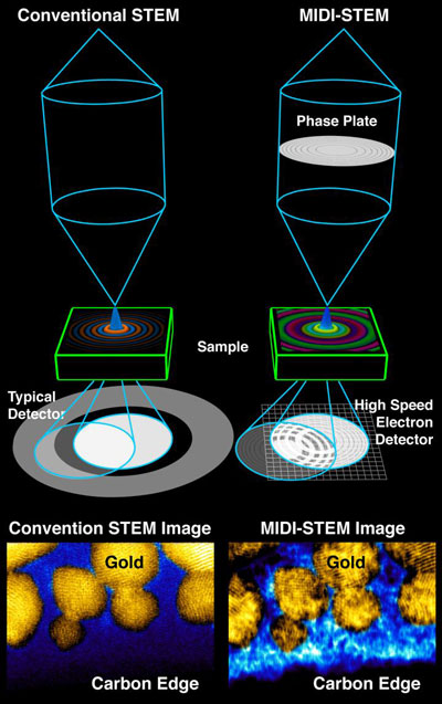
MIDI-STEM Setup
In MIDI-STEM (right), developed at Berkeley Lab, an electron beam travels through a ringed „phase plate,” producing a high-resolution image (bottom right) that provides details about a sample containing a heavy element (gold) and light element (carbon). Details about the carbon are missing in an image (bottom left) of the sample using a conventional electron imaging technique (ADF-STEM). (Image: Colin Ophus/Berkeley Lab)
The newly demonstrated technique, dubbed MIDI-STEM, for matched illumination and detector interferometry STEM, combines STEM with an optical device called a phase plate that modifies the alternating peak-to-trough, wave-like properties (called the phase) of the electron beam.
This phase plate modifies the electron beam in a way that allows subtle changes in a material to be measured, even revealing materials that would be invisible in traditional STEM imaging.
Another electron-based method, which researchers use to determine the detailed structure of delicate, frozen biological samples, is called cryo-electron microscopy, or cryo-EM. While single-particle cryo-EM is a powerful tool–it was named as science journal Nature’s 2015 Method of the Year –it typically requires taking an average over many identical samples to be effective. Cryo-EM is generally not useful for studying samples with a mixture of heavy elements (for example, most types of metals) and light elements like oxygen and carbon.
„The MIDI-STEM method provides hope for seeing structures with a mixture of heavy and light elements, even when they are bunched closely together,” said Colin Ophus, a project scientist at Berkeley Lab’s Molecular Foundry and lead author of a study, published Feb. 29 in Nature Communications („Efficient linear phase contrast in scanning transmission electron microscopy with matched illumination and detector interferometry”), that details this method.
If you take a heavy-element nanoparticle and add molecules to give it a specific function, conventional techniques don’t provide an easy, clear way to see the areas where the nanoparticle and added molecules meet.
„How are they aligned? How are they oriented?” Ophus asked. „There are so many questions about these systems, and because there wasn’t a way to see them, we couldn’t directly answer them.”
While traditional STEM is effective for „hard” samples that can stand up to intense electron beams, and cryo-EM can image biological samples, „We can do both at once” with the MIDI-STEM technique, said Peter Ercius, a Berkeley Lab staff scientist at the Molecular Foundry and co-author of the study.
The phase plate in the MIDI-STEM technique allows a direct measure of the phase of electrons that are weakly scattered as they interact with light elements in the sample. These measurements are then used to construct so-called phase-contrast images of the elements. Without this phase information, the high-resolution images of these elements would not be possible.
In this study, the researchers combined phase plate technology with one of the world’s highest resolution STEMs, at Berkeley Lab’s Molecular Foundry, and a high-speed electron detector.
They produced images of samples of crystalline gold nanoparticles, which measured several nanometers across, and the super-thin film of amorphous carbon that the particles sat on. They also performed computer simulations that validated what they saw in the experiment.
The phase plate technology was developed as part of a Berkeley Lab Laboratory Directed Research and Development grant in collaboration with Ben McMorran at University of Oregon.
The MIDI-STEM technique could prove particularly useful for directly viewing nanoscale objects with a mixture of heavy and light materials, such as some battery and energy-harvesting materials, that are otherwise difficult to view together at atomic resolution.
It also might be useful in revealing new details about important two-dimensional proteins, called S-layer proteins, that could serve as foundations for engineered nanostructures but are challenging to study in atomic detail using other techniques.
In the future, a faster, more sensitive electron detector could allow researchers to study even more delicate samples at improved resolution by exposing them to fewer electrons per image.
„If you can lower the electron dose you can tilt beam-sensitive samples into many orientations and reconstruct the sample in 3-D, like a medical CT scan. There are also data issues that need to be addressed,” Ercius said, as faster detectors will generate huge amounts of data. Another goal is to make the technique more „plug-and-play,” so it is broadly accessible to other scientists.
Source: Lawrence Berkeley National Laboratory

Read more: New form of electron-beam imaging can see elements that are ‘invisible’ to common methods

Dispozitive electronice extensibile care au o lungime cvadruple(Stretchable electronics that quadruple in length)

Și pentru că urmează forma și mișcarea corpului uman, ar putea fi folosită pentru senzori concepuți pentru a monitoriza anumite funcții biologice

sti (6)

Un nou dispozitiv ar putea pune capăt agoniei pentru mii de oameni(New device could end blood test agony for thousands)

a creat un senzor productiv în masă, care poate detecta nivelele de amoniac în respirație – o descoperire care ar putea elimina utilizarea acelor în rândul a mii de pacienți

s40

Șocant roz: un test inexpresiv pentru atacurile cu arme chimice(Shocking Pink: An Inexpresive Test for Chemical Weapon Attacks)

ar putea inspira oamenii de stiinta pentru a dezvolta un instrument de cost pentru a detecta rapid arme chimice in aer; au fost în măsură să detecteze prezența unui agent nervos legat de gazul sarin la un nivel scăzut

20 sept

Detectarea în timp real și fără etichete a virusurilor singulare în soluții complexe (Real-time and label-free detection of single viruses in complex solutions)

Cu senzorul nostru putem vedea mii de virusi sau nanoparticule individuale in timp real in timp ce se afla in mediul natural, cum ar fi serul sau plasma”, spune Scherr. Acest lucru ne permite sa luam masuratori dinamice si sa investigam vizual un numar mare de virusi in solutie intr-un mod care nu a fost anterior posibil.
In plus, adaugand, ca sistem de detectie, abordarea noastra elimina practic orice preparare a probelor. Deoarece agentii patogeni virale sunt vizualizati direct, fara etichete, detectati si discriminati de la un alt zgomot care poate interfera in solutia tinta, Necesar.”

Posted: Feb 05, 2016

Real-time and label-free detection of single viruses in complex solutions

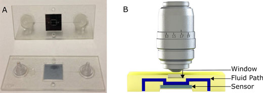
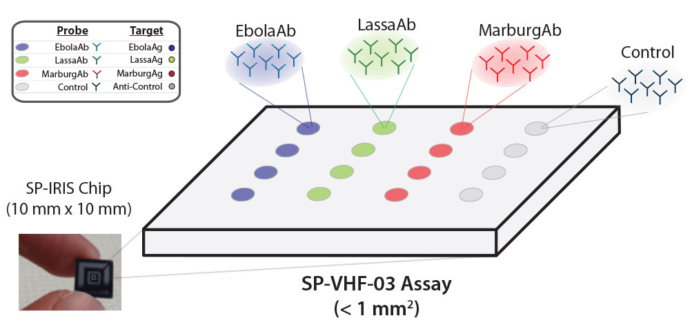
(Nanowerk Spotlight) Every outbreak of a deadly or dangerous virus somewhere in the world – like last year the Ebola virus in West Africa, or just now the Zika virus in Latin America – highlights the importance of rapid detection and accurate diagnosis in health care and preventative medicine. Early detection of these diseases is a critical tool in helping control the virus and save lives.The problem is that many virus detection platforms, including conventional fluorescent label-based ones, have limitations because they are time-intensive and not easily compatible with point-of-care use without the existence of significant infrastructure and expert staff. Case in point is electron microscopy, frequently used for the direct imaging of viruses and nanoparticles, but not suitable for field operations.”Various novel optical sensor systems have been developed in an attempt to meet the needs of point-of-care environments,” M. Selim Ünlü, Distinguished Professor of Engineering in the Optical Characterization and Nanophotonics Laboratory (OCN Lab) at Boston University, tells Nanowerk. „Each of these optical sensors has unique benefits, but none has truly filled the gap to provide robust, direct, and chemically specific high-throughput single-particle visualization in a complex sample. There remains a need for a bridging technology between traditional wide-field microscopy and high-resolution electron microscopy.”In new work, Ünlü’s group and their collaborators have mated an interferometric reflectance imaging sensor developed in their lab with a microfluidic cartridge that allows them to dynamically image the sensor and visualize very small nanoparticles in solution.The researchers reported their findings in the January 13, 2016 online edition of ACS Nano („Real-Time Capture and Visualization of Individual Viruses in Complex Media”).This is the first technique capable of specifically visualizing label-free single viruses in complex solutions in real-time.label-free virus imaging(A) Picture of the first generation polymeric cartridge used for virus and nanoparticle imaging. (B) Cross section model which demonstrates the fluidic path (in blue), the sensor (in gray) and the chip and window (in yellow) not to scale. (Reprinted with permission by American Chemical Society)”We developed a simple to use tool that extends the range of light microscopy to smaller size particles allowing visualization of viruses and nanoparticles that used to require specialized liquid electron microscopy techniques,” notes Steven M. Scherr, a Graduate Research Assistant in the OCN Lab and first author of the paper.The OCN team and its collaborators have spent the past several years advancing a rapid, label-free, chip-scale photonic device that can provide affordable, simple, and accurate on-site detection. They first demonstrated the concept back in 2010 (Nano Letters, „High-Throughput Detection and Sizing of Individual Low-Index Nanoparticles and Viruses for Pathogen Identification”). In 2014, a team led by Ünlü and MED associate professor of microbiology John H. Connor followed this up with a study where they showed the capture and imaging of Ebola and Marburg surrogates using this technology (ACS Nano, „Digital sensing and sizing of vesicular stomatitis virus pseudotypes in complex media: a model for Ebola and Marburg detection”).Now, with this new work, they have refined their instrumentation to allow the simultaneous detection of multiple viruses in blood serum samples—including viruses genetically modified to mimic the behavior of Ebola and the Marburg virus.”With our sensor we can see thousands of individual viruses or nanoparticles in real-time while they are still in a natural environment, such as serum or plasma,” says Scherr. „This lets us take dynamic measurements and visually investigate a large number of viruses in solution in a way that was previously not possible.””Furthermore” he adds, „as a detection system, our approach eliminates virtually all sample preparation. Since the viral pathogens are directly (without labels) visualized, detected, and discriminated from other potentially interfering noise in the target solution, no wash step is needed.”The team has named their prototype diagnostic device the Single-Particle Interferometric Imaging Sensor (SP-IRIS). It allows for the study of unmodified viruses using visible light microscopy. It works by shining light from multi-color LED sources on viruses that are bound to the sensor surface by a coating of virus-specific antibodies. Interference of light reflected from the surface is modified by the presence of the viruses, producing a distinct signal that reveals the size and shape of each virus.The scientists point out that this technique can help bridge the gap between light microscopy and electron microscopy and be applied to both research and diagnostic applications. This tool will let researchers explore populations of synthetic and bio-nanoparticles (viruses, cellular vesicles, etc.) in solution. The sensor can also be used as a rapid and sensitive diagnostic tool.In a multiplexed detection configuration, Ebola, Marburg and Lassa antibodies on the SP-IRIS surface capture corresponding viruses specificallyIn a multiplexed detection configuration, Ebola, Marburg and Lassa antibodies on the SP-IRIS surface capture corresponding viruses specifically. As shown in the images produced by the device, SP-IRIS then identifies and counts each virus particle and classifies it based on its size. (Image: NexGen Arrays) (click on image to enlarge)”We are continuing to develop this as a rapid viral hemorrhagic fever test,” says Scherr. „This technique lets us test for Ebola as well as several other similar diseases in a single test that is both fast and sensitive and requires less sample preparation than other highly sensitive techniques.”The team’s collaborators at The University of Texas Medical Branch at Galveston (Geisbert Lab) will begin testing this cartridge with bona fide Ebola samples in the near future. The experiments will be done using the in-liquid imaging approach described in the manuscript using an automated reader created by Nexgen Arrays, a spinout company that commercializes the SP-IRIS platform.”We would like to see a highly multiplexed virus detection panel that can differentiate between a number of viruses that present with similar symptoms available in an easy-to-use disposable cartridge platform,” adds Ünlü. „Also, our technique allows for characterization of viruses. An exciting new application area for our technology is the quality control application for the emerging oncolytic viruses.”
Video: This movie demonstrates virus binding and single virus detection. It represents the actual binding sped up by a factor of 100. The initial images at the beginning of the experiment show very few particles present on the sensor surface. Accumulation of virus begins rapidly and is sustained for the 60 minute experiment. The movie was created using the images acquired from the SP-IRIS sensor system with minimal postprocessing (AVI). (Video: Optical Characterization and Nanophotonics Laboratory at Boston University)The team wants to continue to push the limit on the smallest particles they can see with this technique and improve the cartridge to make the test easy enough for anyone to use. Although imaging ultra-small particles in solution is difficult, optical detection remains an invaluable tool.By Michael is author of two books by the Royal Society of Chemistry: Nano-Society: Pushing the Boundaries of Technology and Nanotechnology:

Read more: Real-time and label-free detection of single viruses in complex solutions

Simțiți spații cu „pălăria de proximitate”(Feeling spaces with the „proximity hat” )

Senzorul ultrasonic, bateriile și tampoanele de presiune sunt părți ale noului sistem care poate fi pus pe cap ca o pălărie sau bandă de susținere

101 sept

Tehnica de creștere nanosheet ar putea revoluționa producția de nanomateriale

Datorită proprietăților chimice, agentul tensioactiv se asamblează într-un singur strat la suprafața lichidului, cu ioni sulfați încărcați negativ în direcția lichidului. Acești ioni sulfați extrag ionii de zinc încărcați pozitiv din interiorul lichidului la suprafață și în decurs de câteva ore sugerează suficient ioni de zinc pentru a forma nanopreți de oxid de zinc continuu doar câteva straturi atomice groase.

Posted: Jan 29, 2016

Nanosheet growth technique could revolutionize nanomaterial production

(Nanowerk News) After six years of painstaking effort, a group of University of Wisconsin-Madison materials scientists believe the tiny sheets of the semiconductor zinc oxide they’re growing could have huge implications for the future of a host of electronic and biomedical devices.

The group – led by Xudong Wang, a UW-Madison professor of materials science and engineering, and postdoctoral researcher Fei Wang – has developed a technique for creating nearly two-dimensional sheets of compounds that do not naturally form such thin materials. It is the first time such a technique has been successful.
The researchers described their findings in the journal Nature Communications („Nanometre-thick single-crystalline nanosheets grown at the water–air interface”).
nanosheet
The new nanoscale manufacturing process draws zinc to the surface of a liquid, where it forms sheets just a few atoms thick. (Image: Xudong Wang)
Essentially the microscopic equivalent of a single sheet of paper, a 2-D nanosheet is a material just a few atoms thick. Nanomaterials have unique electronic and chemical properties compared to identically composed materials at larger, conventional scales.
„What’s nice with a 2-D nanomaterial is that because it’s a sheet, it’s much easier for us to manipulate compared to other types of nanomaterials,” says Xudong Wang.
Until now, materials scientists were limited to working with naturally occurring 2-D nanosheets. These natural 2-D structures include graphene, a single layer of graphite, and a limited number of other compounds.
Developing a reliable method to synthesize and manufacture 2-D nanosheets from other materials has been a goal of materials researchers and the nanotechnology industry for years.
In their technique, the UW-Madison team applied a specially formulated surfactant – a detergent-like substance – onto the surface of a liquid containing zinc ions.
Due to its chemical properties, the surfactant assembles itself into a single layer at the surface of the liquid, with negatively charged sulfate ions pointed in the direction of the liquid. Those sulfate ions draw the positively charged zinc ions from within the liquid to the surface, and within a couple hours enough zinc ions are drawn up to form continuous zinc oxide nanosheets only a few atomic layers thick.
Xudong Wang first had the idea for using a surfactant to grow nanosheets during a lecture he was giving in a course on nanotechnology in 2009.
„The course includes a lecture about self-assembly of monolayers,” he says. „Under the correct conditions, a surfactant will self-assemble to form a monolayer. This is a well-known process that I teach in class. So while teaching this, I wondered why we wouldn’t be able to reverse this method and use the surfactant monolayer first to grow the crystalline face.”
After five years of trial and error with different surfactant solutions, the idea paid off.
„We are very excited about this,” says Xudong Wang. „This is definitely a new way to fabricate 2-D nanosheets, and it has great potential for different materials and for many different applications.”
Already, the researchers have found that the 2-D zinc oxide nanosheets they’ve grown are able to function as semiconductor transistors called a p-type, the opposite electronic behavior of naturally occurring zinc oxide. Researchers have for some time attempted to produce zinc oxide with reliable p-type semiconductor properties.
Zinc oxide is a very useful component of electronic materials, and the new nanosheets have potential for use in sensors, transducers and optical devices.
But the zinc oxide nanosheets are only the first of what could be a revolution in 2-D nanomaterials. Already, the UW-Madison team is applying its surfactant method to growing 2-D nanosheets of gold and palladium, and the technique holds promise for growing nanosheets from all sorts of metals that wouldn’t form them naturally.
„It brings a lot of new functional material to this 2-D material category,” Wang says.
Source: University of Wisconsin-Madison

Read more: Nanosheet growth technique could revolutionize nanomaterial production