
Nanosenzorul senzitiv se trezește numai în prezența unui semnal de interes (Dormant nanosensor awakens only in the presence of a signal of interest )

Construiți un senzor minuscul care detectează o semnătură de lungimi de undă în infraroșu (IR) caracteristice unei conducte de esapament fierbinți, unui foc de lemn sau chiar unei ființe umane. Proiectați senzorul astfel încât acesta să rămână în stare latentă și nesupravegheată, dar întotdeauna în stare de alertă, chiar și ani de zile, fără a atrage energia bateriei. Și construiți senzorul astfel încât actul de detecție în sine poate iniția emiterea unui semnal care avertizează războinicii, pompierii sau alții că a fost detectat un „semnal de interes”. Este doar o tehnologie de inteligență, recunoaștere și supraveghere (ISR), care poate spori gradul de conștientizare a situației, reducând în același timp necesitatea unor misiuni de întreținere potențial periculoase pentru înlocuirea bateriilor de descărcare. „Ceea ce este cu adevărat interesant în ceea ce privește tehnologia Northeastern IR sensor este că, spre deosebire de senzorii convenționali, acesta consumă zero putere de stand-by atunci când lungimile de undă IR care trebuie detectate nu sunt prezente”, a declarat Troy Olsson, manager al programului N-ZERO în DARPA’s Microsystems Technology Office. „Când aceste lungimi de undă IR sunt prezente și afectează senzorul IR al echipei Northeastern, energia din sursa IR încălzește elementele senzoriale care, la rândul lor, determină mișcarea fizică a componentelor senzorilor cheie. Aceste mișcări au ca rezultat închiderea mecanică a elementelor de circuit deschis, în alt mod, ceea ce duce la semnalele de detectare a semnăturii IR. „

Posted: Sep 12, 2017

Dormant nanosensor awakens only in the presence of a signal of interest

(Nanowerk News) Here’s your task. Build a tiny sensor that detects a signature of infrared (IR) wavelengths characteristic of a hot tailpipe, a wood fire, or perhaps even a human being. Design the sensor so that it can remain dormant and unattended but always alert, even for years, without drawing on battery power. And build the sensor so that the act of detection itself can initiate the emission of a signal that alerts warfighters, firefighters, or others that a “signal-of-interest” has been detected. It’s just the sort of intelligence, reconnaissance, and surveillance (ISR) technology that can increase situational awareness while minimizing the need for potentially dangerous maintenance missions to replace run-down batteries.

Reporting in the journal Nature Nanotechnology („Zero Power Infrared Digitizers Based on Plasmonically-enhanced Micromechanical Photoswitches”), a research team at Northeastern University, led by Electrical and Computer Engineering Associate Professor Matteo Rinaldi, reports pulling off this tall order of DARPA’s Near Zero Power RF and Sensor Operation (N-ZERO) program with a device the Boston team refers to as a “plasmonically-enhanced micromechanical photoswitch.”
micro features of multiple, wavelength-specific sensor patches
The micrograph features the multiple, wavelength-specific sensor patches that enable this N-ZERO device to capture infrared signatures of specific heat-emitting sources. (Image: DARPA)
“What is really interesting about the Northeastern IR sensor technology is that, unlike conventional sensors, it consumes zero stand-by power when the IR wavelengths to be detected are not present,” said Troy Olsson, manager of the N-ZERO Program in DARPA’s Microsystems Technology Office. “When those IR wavelengths are present and impinge on the Northeastern team’s IR sensor, the energy from the IR source heats the sensing elements which, in turn, causes physical movement of key sensor components. These motions result in the mechanical closing of otherwise open circuit elements, thereby leading to signals that the target IR signature has been detected.”
The sensor is a showcase of clever physics and engineering, including a grid of nanoscale patches whose specific dimensions limit them to absorb only particular IR wavelengths. “The charge-based excitations, called plasmons (that can be thought of somewhat like ripples on the surface of water), are highly localized below the nanoscale patches and effectively trap specific wavelengths of light into the ultra-thin structure, inducing a relatively large and swift spike in its temperature,” Rinaldi explained. These temperature spikes, in turn, lead to an upstream sequence of events that culminates in circuit-completing deformations of other parts of the sensor.
“The technology features multiple sensing elements—each tuned to absorb a specific IR wavelength,” Olsson noted. “Together, these combine into complex logic circuits capable of analyzing IR spectrums, which opens the way for these sensors to not only detect IR energy in the environment but to specify if that energy derives from a fire, vehicle, person or some other IR source.”
Consider the identification of vehicles from their IR emissions. Engines that burn gasoline or diesel fuels emit specific compounds in their exhaust gases. Among these compounds are CO2, CO, H2O, various oxides of nitrogen and sulfur (NOx and SOx, respectively), and hydrocarbons such as methane. “As a result, the infrared emission spectra of the heated tailpipe gases coming out of vehicles such as trucks, cars or aircraft can by themselves act as a signature specific to a vehicle type,” explained Zhenyun Qian, who has been working with Rinaldi and other research team members on the N-ZERO program.
A primary goal of the N-ZERO program is to develop fundamental technologies that open the way to new and more capable sensor systems relevant to national security. The NU team points out in its Nature Nanotechnology paper that the same technology could become important over the coming years as the Internet of Things expands to include hundreds of billions of devices, ranging from cars, to appliances, to remotely deployed sensors. “The capability of consuming power only when useful information is present will result in nearly unlimited duration of operation for unattended sensors deployed to detect infrequent but time-critical events, with a groundbreaking impact on the proliferation of the Internet of Things,” the Northeastern researchers predict in their paper.
Source: DARPA

Read more: Dormant nanosensor awakens only in the presence of a signal of interest
Extinderea limitelor conductorilor elastici(Stretching the limits of elastic conductors)

Noul material, produs sub formă de cerneală ca o pastă, pot fi imprimate în diferite modele pe textile și suprafețe de cauciuc ca cabluri alungibil pentru dispozitivele purtabile care încorporează senzori, precum și a da funcții ale pielii cum ar fi umane exterioare robotului ( Nature Materials , „Printable conductori elastici prin formarea in situ a nanoparticulelor de argint din fulgi de argint ” ).

Posted: Sep 12, 2017

Stretching the limits of elastic conductors

(Nanowerk News) A newly developed printable elastic conductor retains high conductivity even when stretched to as much as five times its original length, says a Japanese team of scientists. The new material, produced in paste-like ink form, can be printed in various patterns on textiles and rubber surfaces as stretchable wiring for wearable devices incorporating sensors, as well as give human skin-like functions to robot exteriors (Nature Materials, „Printable elastic conductors by in situ formation of silver nanoparticles from silver flakes”).

LED-integrated pressure-sensing glove
LED-integrated pressure-sensing glove. Each fingertip pressure sensor mounted on this glove is connected to an LED. The intensity of the LEDs varies according to the pressure applied by the fingertips. The glove makes it possible to ascertain degrees of pressure that are difficult to obtain just by examining images. (Image: Someya Group, The University of Tokyo)
The development of wearable devices such as those monitoring a person’s health or physical performance, like heart rate or muscle activity, is currently underway with some products already on the market. Moreover, with the advent of robots in areas such as health care and retail, in addition to manufacturing, future applications for sensitive elastic conductive material that can withstand high strain from stretching are likely to increase at a fever pitch.
„We saw the growing demand for wearable devices and robots,” says Professor Takao Someya at the University of Tokyo’s Graduate School of Engineering, who supervised the current study. „We felt it was very important to create printable elastic conductors to help meet the need and realize the development of the products,” he adds.
To achieve a high degree of stretchability and conductivity, the researchers mixed four components to create their elastic conductor. They found that their conductive paste consisting of micrometer-sized silver (Ag) flakes, fluorine rubber, fluorine surfactant—commonly known as a substance that reduces surface tension in liquid—and organic solvent to dissolve the fluorine rubber markedly outperformed the elastic conductor they had previously developed in 2015.
Without stretching, printed traces of the new conductor recorded 4,972 siemens per centimeter (S/cm), high conductivity using the common measure for assessing electrical conductance. When stretched by 200 percent, or to three times its original length, conductivity measured 1,070 S/cm, which is nearly six times the value of the previous conductor (192 S/cm). Even when stretched by 400 percent, or to five times its original length, the new conductor retained high conductivity of 935 S/cm, the highest level recorded for this amount of stretching.
Magnification by a scanning electron microscope (SEM) and transmission electron microscope (TEM) showed that the high performance of the conductor was due to the self-formation of silver (Ag) nanoparticles—one-thousandth the size of the Ag flakes and dispersed uniformly between the flakes in the fluorine rubber—after the conductive composite paste was printed and heated. „We did not expect the formation of Ag nanoparticles,” comments Someya on their surprising discovery.
Furthermore, the scientists found that by adjusting variables like the molecular weight of the fluorine rubber, they could control the distribution and population of nanoparticles, while the presence of surfactant and heating accelerated their formation and influenced their size.
To demonstrate the feasibility of the conductors, the scientists fabricated fully printed stretchable pressure and temperature sensors – that can sense weak force and measure heat close to body and room temperatures – wired with the printable elastic conductors on textiles. The sensors, which can be installed easily by laminating onto surfaces by hot pressing with heat and pressure, took precise measurements even when stretched by 250 percent. This is enough to accommodate high-stress flexible areas such as elbows and knees on conformable, form-fitting sportswear or joints on robotic arms often designed to surpass human capabilities and thus undergo higher strain.
The new material, which is durable and suitable for high-capacity printing methods like stencil or screen printing that can cover large surface areas, points to easy installation, and its properties of forming Ag nanoparticles (which are a fraction of the cost of Ag flakes) when printed provide an economical alternative for realizing a wide range of applications for wearables, robotics, and deformable electronic devices. The team is now exploring substitutes for Ag flakes to further reduce costs, while they are also looking at other polymers, like nonfluorine rubbers, and various combinations of materials and processes to fabricate elastic conductors with similar high performance.
Source: University of Tokyo

Read more: Stretching the limits of elastic conductors

Nanoparticulele polimerice fluorescente îndreaptă degetul spre urme de dispozitive explozive (Fluorescent polymer nanoparticles point the finger at traces of explosive devices )

Loturile de bombe ar putea fi contracarate cu ajutorul unui sistem portabil pentru detectarea urmelor de explozivi exploziva folosind nanoparticule polimerice fluorescente, dezvoltat de A * STAR. Imprimate pe hârtie, acești polimeri prezintă o performanță de detecție a explozivului mult mai robustă decât materialele anterioare cu proprietăți similare ( Polymer Chemistry , poli (trifenil ethene) și poli (tetraphenyl ethene): sinteza, proprietatea de emisie indusă de agregare și aplicarea ca hârtie senzori pentru detectarea efectivă a nitro-compușilor ” ).
Multe metode au fost dezvoltate pentru a detecta urme de explozivi de mare intensitate, cum ar fi trinitrotoluenul (TNT), dar majoritatea necesită instrumente analitice de laborator, cum ar fi detectorii de absorbție UV sau spectrometrele de masă, spune Jianwei Xu de la Institutul A * Engineering, care a condus lucrarea. „Ne-am propus să dezvoltăm o alternativă portabilă, rapidă, ieftină și foarte sensibilă”.

Posted: Sep 08, 2017

Fluorescent polymer nanoparticles point the finger at traces of explosive devices

(Nanowerk News) Bomb plots could be thwarted with the help of a portable system for detecting traces of high explosives using fluorescent polymer nanoparticles, developed by A*STAR. Coated on to paper, these polymers display an explosive-detection performance far more robust than previous materials with similar properties (Polymer Chemistry, „Poly(triphenyl ethene) and poly(tetraphenyl ethene): synthesis, aggregation-induced emission property and application as paper sensors for effective nitro-compounds detection”).

Many methods have been developed to detect traces of high explosives such as trinitrotoluene (TNT), but most require large, lab-based analytical instruments such as UV absorption detectors or mass spectrometers, says Jianwei Xu from the A*STAR Institute of Materials Research and Engineering, who led the work. “We aimed to develop a portable, quick, inexpensive and highly sensitive alternative.”
polymer-coated polymer readily could detect fingerprints contaminated with traces of four common high explosives
The polymer-coated polymer readily could detect fingerprints contaminated with traces of four common high explosives, including TNT.
Xu focused on fluorescent polymers whose light emission dims when exposed to vapors of molecules such as TNT that contain ‘nitro-groups’ — the nitrogen-rich structure that give high explosives their energetic properties.
Although explosive-detecting fluorescent polymers have been developed before, there have been obstacles to their practical use, Xu explains. Some lost part of their fluorescence in solid form through a process called aggregation-caused quenching. Others lacked the necessary porosity for explosives vapor penetration, only retaining an effective response when formed in layers of around 2.5 nanometers — so thin, the sensor would be very difficult to fabricate cheaply.
Xu and his colleagues have been developing polymers that, rather than losing their light emission in the solid state, become brighter, an effect known as aggregation-induced emission (AIE). “Our previous research demonstrated that porous films obtained from AIE active copolymers show a strong response to the vapor of nitro-compounds,” says Xu.
The team has now developed two new polymers, poly(triphenyl ethene) (PTriPE) and poly (tetraphenyl ethene) (PTPE), designed to maximize AIE, porosity and nitro group sensitivity. The polymers’ multiple bulky phenyl groups help keep them rigid and maximize light emission following aggregation. But in the presence of nitro-groups, electron transfer between polymer and analyte rapidly quenches the light.
“Paper sensors fabricated by absorbing the polymer nanoparticles on to filter paper showed high sensitivity for nitro-compound particles,” says Xu. PTriPE proved to be the pick of the pair, detecting TNT at a concentration of five parts per billion, even in polymer layers 1000 nanometers thick.
“This technology could be used at airports, ports and for border control for detecting explosives in any explosive-contaminated containers, clothing, boxes or bags,” says Xu. “We are seeking co-operation with industry to commercialize this technology.”
Source: A*STAR

Read more: Fluorescent polymer nanoparticles point the finger at traces of explosive devices

Fotodiodele organice – detectori mai economici pentru regiunea NIR(Organic photodiodes – more economical detectors for the NIR region )

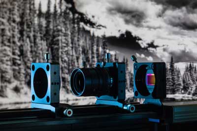
Senzor de imagine bazat pe fotodiodele organice pe siliciu, în aplicații tipice pentru camere. Context: Imagine NIR. (Imagine: Fraunhofer FEP, Fotograf: Jürgen Lösel)
Imaginile CMOS pe bază de siliciu convenționale sunt limitate la o regiune de lungime de undă restricționată din motive tehnologice fundamentale. Acestea sunt de obicei setate pe segmentul vizibil al spectrului. Dacă doriți să detectați lumina în infraroșu apropiat (NIR), cu toate acestea, soluții hibride, cum ar fi combinații de arsenid de iniu galiu (InGaAs) cu CMOS sunt, de obicei, recurs la.
Cu toate acestea, fabricarea acestor tipuri de soluții hibride este considerabil mai costisitoare și mai predispusă la defecte decât fabricarea utilizând procese standard CMOS. Aici fotodiodele organice oferă o alternativă. Straturile organice pot fi integrate pur și simplu la nivelul plachetelor și, prin urmare, sunt economice. În același timp, acestea pot avea, de asemenea, o sensibilitate ridicată în afara regiunii vizibile a lungimii de undă, în funcție de sistemul de materiale selectat

Posted: Sep 05, 2017

Organic photodiodes – more economical detectors for the NIR region

(Nanowerk News) The Fraunhofer Institute for Organic Electronics, Electron Beam and Plasma Technology FEP will be introducing a new generation of organic photodiodes on silicon substrates (OPD-on-silicon) during the SEMI European Imaging & Sensors Summit 2017, September 20-22 in Grenoble, France, at MINATEC, Booth 42.

Optical sensors are pervasive. Domestic life as well as the industrial environment are hard to imagine without them. For example, digital cameras using CMOS detectors have been indispensable vacation companions for many years, while in industry they serve as a simple and economical solution for automated image processing (such as in quality control applications, remote presence and position recognition and counting in conveyor systems, and object recognition in warehousing logistics). They can also be employed in medical engineering for diagnostic image processing. There are many future applications in the field of autonomous vehicles that are already foreseeable today.
Image sensor based on organic photodiodes on silicon in typical camera application
Image sensor based on organic photodiodes on silicon in typical camera application. Background: NIR image. (Image: Fraunhofer FEP, Photographer: Jürgen Lösel)
Conventional silicon-based CMOS imagers are limited to a restricted wavelength region for fundamental technological reasons. They are usually set to the visible segment of the spectrum. If you want to detect light in the near-infrared (NIR), however, hybrid solutions such as combinations of indium gallium arsenide (InGaAs) with CMOS are usually resorted to.
Nevertheless, the manufacture of these kinds of hybrid solutions is considerably more costly and more prone to defects than fabrication using standard CMOS processes. This is where organic photodiodes offer an alternative. The organic layers can be integrated simply at wafer level and are therefore economical. Simultaneously, they also may have high sensitivity outside the visible wavelength region, depending on the system of materials selected.
The Fraunhofer FEP has extensive experience in integrating organic layers on CMOS wafers. Diverse OLED microdisplays (high-resolution, low power, embedded image sensors, …) as well as sensors for fingerprint, flow, and photoelectric sensing applications have already been developed and fabricated.
“We will be debuting an organic photodiode array with SVGA resolution at SEMI European Imaging & Sensors Summit 2017. That means 800 × 600 pixels available for detection applications”, explains Philipp Wartenberg, head of the IC and System Design department at Fraunhofer FEP. “We have demonstrated that it is fundamentally feasible to fabricate a high-resolution organic photodiode matrix at this order of magnitude. It is sensitive at wavelengths up to 1,000 nanometers. We are able to develop customer- and application-specific organic photodiodes with optimized properties for the concrete application through appropriate adaption of material.”
The demonstrated image sensors were fabricated completely at wafer-level and therefore already under near-production conditions. With its extended region of sensitivity, the imager can be employed over the entire bandwidth of conventional applications in industry, automobiles, and medicine. They could be used for quality control of foodstuffs, as fingerprint sensors, and in biomedical tests, for example.
The scientists are now making the new technology available to industrial partners in order to jointly develop and produce optimized organic photodiodes and arrays as image sensors for their respective applications.
Source: Fraunhofer Institute for Organic Electronics, Electron Beam and Plasma Technology
Subscribe to a free copy of one of our daily
Nanowerk Newsletter Email Digests
with a compilation of all of the day’s news.

Read more: Organic photodiodes – more economical detectors for the NIR region

Nanoimateriale de carbon mai sigure, prin design (Nanoparticles limit damage in spinal cord injury)

Nanowerk News ) Nanomaterialele de carbon (CNM) sunt o clasă de nanomateriale fabricate care pot fi utilizate pentru multe aplicații de mediu, inclusiv tratarea apei și detectarea și remedierea contaminanților. În timp ce sunt apreciați pentru abilitatea lor de a detecta, îndepărta sau degrada contaminanții din mediul înconjurător, CNM-urile nu dispar doar după ce sunt folosite.
„Ca orice substanță chimică care persistă în mediul înconjurător, există îngrijorări cu privire la impactul asupra organismelor și sistemelor care rezultă din pericolul inerent al materialului, al produselor sale de degradare și al potențialului său de a se bioacumula – sau se acumulează în corpurile vieții,

Posted: Sep 05, 2017

Nanoparticles limit damage in spinal cord injury

(Nanowerk News) After a spinal cord injury, a significant amount of secondary nerve damage is caused by inflammation and internal scarring that inhibits the ability of the nervous system to repair itself.

A biodegradable nanoparticle injected after a spinal cord trauma prevented the inflammation and internal scarring that inhibits the repair process, reports a new Northwestern Medicine study.
As a result, mice with a spinal cord injury receiving the nanoparticle injection were able to walk better after the injury than those that didn’t receive it.
The treatment could potentially limit secondary damage to the spinal cord in humans after an injury, if administered a few hours after the accident in an emergency room or by paramedics in an ambulance.
“It’s not a cure. There is still the original damage, but we were able to prevent the secondary damage,” said co-senior author Dr. Jack Kessler, a professor of neurology at Northwestern University Feinberg School of Medicine and a Northwestern Medicine neurologist. “It’s an exciting potential treatment. We really believe this is something we’ll be able to take to the clinic.”
Further studies would need to confirm the safety of the injected nanoparticle, Kessler said, but he noted scientists haven’t seen any signs of toxicity so far.
The study was published in Neurobiology of Disease („Intravenous immune-modifying nanoparticles as a therapy for spinal cord injury in mice”).
The nanoparticles work by binding to the cells that cause the inflammation — inflammatory monocytes — and diverting them to the spleen. The particles are made of poly(lactic-co-glycolic) acid, a biocompatible substance already approved by the Food and Drug Administration (FDA) for use in re-absorbable sutures.
Developed in the lab of Northwestern scientist Stephen Miller, the particles also are FDA approved as an investigational drug for a new clinical trial in celiac disease.
“The study results suggest nanoparticle infusion could offer a novel and practical potential treatment for human spinal cord injury, a condition for which there are currently no effective treatments,” said Miller, the Judy Gugenheim Research Professor of Microbiology-Immunology at Feinberg.
After a spinal cord injury, blood cells that normally couldn’t enter the nervous system breech the protective blood brain barrier and flood the injury site. They release noxious chemicals, called inflammatory cytokines, which call in additional inflammatory blood cells. These cells further damage the central nervous system tissue by causing neuronal cell death and scar formation that blocks recovery from paralysis.
Two types of neurons die. One type — myelin — surrounds the nerve fibers and allows them to carry signals through the nervous system. If the myelin sheath is lost, the cells can no longer conduct signals. The other cells that die are axons, the long fibers extending from the neurons that carry signals from neuron to neuron.
“The new treatment is unusual because it is potentially immediately translatable to human beings,” Kessler said. “All we have to do is literally inject these beads into the blood stream. It doesn’t require surgery or any fancy intervention.”
The tiny beads also are very stable and can be kept in a syringe, Kessler noted. “An emergency medical technician at the site of an accident or somebody in an emergency room when someone is brought in can give this injection immediately,” he said.
Other researchers have tried techniques to block inflammatory monocytes from entering the nervous system after a spinal cord injury, but those methods blocked beneficial and harmful cells. The beneficial cells actually clean up the damage from the trauma and limit the scarring, so previous efforts resulted in only a modest improvement in scarring, cell death and repair.
The nanoparticle technology is being developed commercially by Cour Pharmaceuticals Development Co., which is working with Miller to bring this new approach to patients. Miller is a co-founder of Cour and a member of the scientific advisory board.
Miller also is a member of the Robert H. Lurie Comprehensive Cancer Center of Northwestern University.
Source: By Marla Paul, Northwestern University

Read more: Nanoparticles limit damage in spinal cord injury

Detectarea produselor alimentare contrafăcute(Detection of counterfeit food products )

Senzorul de pH fluorescent rasometric detectează modificările pH-ului în produsele lichide marcate atribuite contaminării bacteriene – o procedură comună în microbiologie

Detection

Grapefină pentru aplicații de detectare (Graphene woven fabrics for sensing application )

Grafenul a atras atenția extinsă datorită proprietăților sale excelente electrice, conductivității termice remarcabile, transparenței înalte, grosimii superioare și zonei mari specifice și, firește, a fost folosit ca material de detectare.
In ACS Applied Materials & Interfaces ( „simultană de înaltă sensibilitate de detectare a temperaturii și umidității cu Grafenul Țesături“ ), cercetatorii raport acum o temperatură și umiditate senzor flexibil (FTHS) din grafen țesături (GWFs) preparate prin depunere chimică din vapori (CVD) .
Senzorul a fost preparat printr-un proces de asamblare strat-cu-strat prietenos cu mediul. În comparație cu filmele de grafeni comune produse de CVD, GWF a fost compus din panglici de micrometru de intercalare cu cristale intercalate și au găuri dreptunghiulare, demonstrând o ultrasensibilitate cu un factor de gabarit de 500 până la deformare cu 2%.Rezultatele simulării și unele dispozitive raportate efectuate de GWF au demonstrat macrostructura și microstructura specială a GWF, care îi promite proprietăți unice și aplicații potențiale diversificate”, concluzioneaza autorii raportului. „Cu un design special, am folosit GWF-uri pentru a produce un senzor flexibil și bifuncțional. FTHS a arătat o sensibilitate ridicată la senzorii de temperatură, o performanță bună de detectare a umidității și o mică interferență reciprocă”.

Posted: Sep 04, 2017

Graphene woven fabrics for sensing application

(Nanowerk News) Graphene has attracted extensive attention because of its excellent electrical properties, outstanding thermal conductivity, high transparency, ultrathin thickness, and large specific area, and naturally, it has been used as a sensing material.

In ACS Applied Materials & Interfaces („Simultaneous High Sensitivity Sensing of Temperature and Humidity with Graphene Woven Fabrics”), researchers now report a flexible temperature and humidity sensor (FTHS) from graphene woven fabrics (GWFs) prepared by chemical vapor deposition (CVD).
The sensor was prepared through an environmentally friendly layer-by-layer assembly process. Compared with the common graphene films produced by CVD, the GWF was composed of criss-crossed interlacing graphene micrometer ribbons and had rectangular holes, demonstrating ultra-sensitivity with a gauge factor of 500 to deformation within 2%.
fabricating a flexible temperature and humidity sensor with graphen woven fabrics
(a) Schematic diagram of assembly steps of the FTHS. Inset: photograph of as-prepared FTHS. (b) Mechanism for temperature sensing. (c) Mechanism for humidity sensing. (© ACS) (click on image to enlarge)
The researchers found that the substrate, the length-width ratio of GWF, and the time of the oxygen plasma treatment greatly influenced the sensitivity of the temperature-sensing part.
„Simulation results and some reported devices made by GWF have proved the special macrostructure and microstructure of GWF, which promise it unique properties and diversified potential applications,” the authors conclude their report. „With a special design, we used GWFs to produce a flexible and bifunctional sensor. The FTHS showed high sensitivity in temperature sensing, good humidity sensing performance, and little mutual interference.”
By Michael is author of two books by the Royal Society of Chemistry: N

Read more: Graphene woven fabrics for sensing application

Sistemul de cipuri nanofotonice măsoară lumina de la o singură celulă bacteriană pentru a permite detectarea chimică portabilă ( Nanophotonic chip system measures light from a single bacterial cell to enable portable chemical detection )

Noul sistem, descris în jurnalul Nano Letters ( „Nanoscale Plasmonic V-Groove Waveguides pentru interogarea celulelor bacteriene fluorescente unice” ), deschide calea pentru un sistem eficient și portabil on-chip pentru diverse aplicații de detectare pe bază de celule, cum ar fi Ca și detectarea substanțelor chimice în timp real.
construirea unei rețele de ghiduri de undă, diversificarea sistemului pentru a încorpora diferite tipuri de senzori bacterieni pentru detectarea diferitelor analitări biologice sau chimice.

Posted: Aug 30, 2017

Nanophotonic chip system measures light from a single bacterial cell to enable portable chemical detection

(Nanowerk News) Researchers at the Hebrew University of Jerusalem have created a nanophotonic chip system using lasers and bacteria to observe fluorescence emitted from a single bacterial cell. To fix the bacteria in place and to route light toward individual bacterial cells, they used V-groove-shaped plasmonic waveguides, tiny aluminum-coated rods only tens of nanometers in diameter.

The novel system, described in the journal Nano Letters („Nanoscale Plasmonic V-Groove Waveguides for the Interrogation of Single Fluorescent Bacterial Cells”), paves the way for an efficient and portable on-chip system for diverse cell-based sensing applications, such as detecting chemicals in real-time.
Nanoscale Plasmonic V-Groove Waveguides for the Interrogation of Single Fluorescent Bacterial Cells
Top: SEM image of bacteria deposited inside a V-groove waveguide. Bottom: napshot of bacterial fluorescence excitation via free space beam and the coupling of the fluorescence to the waveguide. The two nanocouplers at the end of the waveguide emit about the same intensity of light because they are roughly the same distance from the bacterium. (© ACS)
The field of on-chip photonic devices for biological and chemical sensing applications presents many powerful alternatives to conventional analytical techniques for applications ranging from “lab on a chip” to environmental monitoring. However, these sensing schemes rely mainly on off-chip detection and require a cumbersome apparatus, even when measuring only single cells.
The Hebrew University team looked for ways to integrate all system components, including light sources and detectors, on-chip at the nanoscale. This would result in a lab-on-chip system that is small, portable and can perform sensing in real-time.
To achieve this, they molecularly engineered live bacteria that emit a fluorescent signal in the presence of target compounds. They paired these on-chip with a nanoscale waveguide, which not only served the purpose of guiding light, but also allowed mechanical trapping of individual bacteria within the V-groove.
In three different illumination conditions, they experimentally demonstrated the interrogation of an individualEscherichia coli bacterial cell using a nanoscale plasmonic V-groove waveguide. First, they measured the light emitted from a bacterium flowing on top of the nanocoupler in a liquid environment by allowing the fluorescence from the bacterium to be coupled directly into the waveguide through the nanocoupler. Next, a bacterium was mechanically trapped within the V groove waveguide and was excited by laser directly either from the top or through the nanocoupler. In all cases, significant fluorescence was collected from the output nano coupler into the detector.
The system worked well both in wet environments, where the bacteria are flowing on top of the waveguide, and in dry conditions, where the bacteria are trapped within the waveguide.
The research was led by Prof. Uriel Levy, Director of The Harvey M. Krueger Family Center for Nanoscience and Nanotechnology at the Hebrew University in collaboration with Prof. Shimshon Belkin, at the Hebrew University’s Alexander Silberman Institute of Life Sciences, who genetically engineered the bacterial sensors, and Prof. Anders Kristensen from the Danish Technical University, who was in charge of fabricating the V-groove waveguides. Prof. Levy is the Eric Samson Chair in Applied Science and Technology, and Prof. Belkin is the Ministry of Labor and Social Welfare Chair in Industrial Hygiene, at the Hebrew University.
Unlike the more traditional plasmonic waveguides consisting of either silver or gold, the choice of aluminum was instrumental for being able to guide the fluorescent light emitted from the bacteria all the way to the output nanocoupler. Furthermore, the waveguide dimensions allow for efficient mechanical trapping of the bacteria and the multimode characteristics may become instrumental in gathering more information, e.g., on the specific position and orientation of the bacteria.
The results provide a clear indication of the feasibility of constructing a hybrid bioplasmonic system using live cells. Future work will include the construction of waveguide network, diversifying the system to incorporate different types of bacterial sensors for the detection of various biological or chemical analytes.
Source: Hebrew University of Jerusalem

Read more: Nanophotonic chip system measures light from a single bacterial cell to enable portable chemical detection

Cercetătorii produc țesături inteligente pentru a neutraliza gazul nervos (Researchers produce smart fabric to neutralize nerve gas )

Țesătura constă dintr-un suport de bumbac modificat cu compozite cu nitruri de carbon cu oxid de carbon-BTC MOF / oxidată. Acestea din urmă au fost dezvoltate anterior în laborator și testate ca medii de detoxifiere a agenților nervoși și detectori colorimetrici.
Combinarea Cu-BTC și gC 3 N 4 -ox a condus la un nanocompozit (MOFgCNo x ) de porozitate și chimie eterogene. După depunerea MOFgCNo x pe textilele de bumbac, a fost obținută o țesătură stabilă cu abilitate supremă de detoxifiere fotocatalitică față de surogatul gazului nervos, dimetil clorofosfat.

Posted: Aug 16, 2017

Researchers produce smart fabric to neutralize nerve gas

(Nanowerk News) From the lab of City College of New York chemical engineer and Fulbright Scholar Teresa J. Bandosz comes a groundbreaking development with the potential to thwart chemical warfare agents: smart textiles with the ability to rapidly detect and neutralize nerve gas (Nanoscale Horizons, „Smart textiles of MOF/g-C3N4 nanospheres for the rapid detection/detoxification of chemical warfare agents”).

The fabric consists of a cotton support modified with Cu-BTC MOF/oxidized graphitic carbon nitride composites. The latter were developed in the lab previously and tested as nerve agent detoxification media and colorimetric detectors.
Combining Cu-BTC and g-C3N4-ox resulted in a nanocomposite (MOFgCNox) of heterogeneous porosity and chemistry. Upon the deposition of MOFgCNox onto cotton textiles, a stable fabric with supreme photocatalytic detoxification ability towards the nerve gas surrogate, dimethyl chlorophosphate, was obtained.
The detoxification process was accompanied by a visible and gradual color change, which Bandosz said can be used for the selective detection of chemical warfare agents and for monitoring their penetration inside a protective layer.
„These smart textiles adsorbed almost 7g of CWA surrogate/its detoxification products per gram of Cu. The superior performance was linked to the high dispersion of the MOF crystals on the fibers, and a specific texture promoting the availability of the active copper centers,” said Bandosz, who is seeking funding for additional research.
Source: City College of New York

Read more: Researchers produce smart fabric to neutralize nerve gas

Materialul 2D cu două fețe este primul(2-faced 2D material is a first)

Noul material pe care îl numesc Janus sulfură de molibden seleniu (SMoSe) are o construcție cristalină, cercetătorii spun că pot găzdui un câmp electric intrinsec și care, de asemenea, arată promisiunea producerii catalitice a hidrogenului.Ar putea conduce la numeroase aplicații, cum ar fi un catalizator activ bazat pe plan 2-D, senzori robusti cu piezoelectricitate și actuatori la limita 2-D. ”

Posted: Aug 14, 2017

2-faced 2D material is a first

(Nanowerk News) Like a sandwich with wheat on the bottom and rye on the top, Rice University scientists have cooked up a tasty new twist on two-dimensional materials.

The Rice laboratory of materials scientist Jun Lou has made a semiconducting transition-metal dichalcogenide (TMD) that starts as a monolayer of molybdenum diselenide. They then strip the top layer of the lattice and replace precisely half the selenium atoms with sulfur.
The new material they call Janus sulfur molybdenum selenium (SMoSe) has a crystalline construction the researchers said can host an intrinsic electric field and that also shows promise for catalytic production of hydrogen.
The work is detailed this month in ACS Nano („Janus Monolayer Transition-Metal Dichalcogenides”).
scientists replace all the atoms on top of a three-layer, two-dimensional crystal to make a transition-metal dichalcogenide with sulfur, molybdenum and selenium
Rice University materials scientists replace all the atoms on top of a three-layer, two-dimensional crystal to make a transition-metal dichalcogenide with sulfur, molybdenum and selenium. (Image: Jing Zhang/Rice University)
The two-faced material is technically two-dimensional, but like molybdenum diselenide it consists of three stacked layers of atoms arranged in a grid. From the top, they look like hexagonal rings a la graphene, but from any other angle, the grid is more like a nanoscale jungle gym.
Tight control of the conditions in a typical chemical vapor deposition furnace – 800 degrees Celsius (1,872 degrees Fahrenheit) at atmospheric pressure – allowed the sulfur to interact with only the top layer of selenium atoms and leave the bottom untouched, the researchers said. If the temperature drifts above 850, all the selenium is replaced.
„Like the intercalation of many other molecules demonstrated to have the ability to diffuse into the layered materials, diffusion of gaseous sulfur molecules in between the layers of these Van der Waals crystals, as well as the space between them and the substrates, requires sufficient driving force,” said Rice postdoctoral researcher Jing Zhang, co-lead author of the paper with graduate student Shuai Jia. „And the driving force in our experiments is controlled by the reaction temperature.”
Close examination showed the presence of sulfur gave the material a larger band gap than molybdenum diselenide, the researchers said.
Janus sulfur molybdenum selenium
This image shows top (left) and side views of Janus sulfur molybdenum selenium created at Rice University. Careful control of heating allows sulfur to replace just the top plane of selenium atoms in the new two-dimensional material. (IMage: Jing Zhang/Rice University)
„This type of two-faced structure has long been predicted theoretically but very rarely realized in the 2-D research community,” Lou said. „The break of symmetry in the out-of-plane direction of 2-D TMDs could lead to many applications, such as a basal-plane active 2-D catalyst, robust piezoelectricity-enabled sensors and actuators at the 2-D limit.”
He said preparation of the Janus material should be universal to layered materials with similar structures. „It will be quite interesting to look at the properties of the Janus configuration of other 2-D materials,” Lou said.
Source: Rice University

Read more: 2-faced 2D material is a first