Cercetătorii detectează detectarea gazului la temperatura camerei(Researchers greenlight gas detection at room temperature)

Cercetatorii rusi au dezvoltat un mecanism pentru detectarea hidrogenului molecular folosind lumina verde pentru iluminarea unui senzor compozit nanocristalin bazat pe oxizi de zinc si indiu. Pentru prima dată, acest lucru permite un senzor de gaz care funcționează la temperatura camerei.Astfel de senzori pot fi utilizați pentru a analiza calitatea aerului în aer liber și în spații închise

Posted: Oct 25, 2017

Researchers greenlight gas detection at room temperature

(Nanowerk News) Russian researchers have developed a mechanism for detecting molecular hydrogen using green light to illuminate a nanocrystalline composite sensor based on zinc and indium oxides. For the first time, this enables a gas sensor operating at room temperature. The paper was published in the journal Scientific Reports („Green light activated hydrogen sensing of nanocrystalline composite ZnO-In2O3 films at room temperature”).

Multisensor arrays for determining gas mixture composition are currently being developed. These are monitoring systems incorporating multiple sensors that target individual gases. Such sensors can be used to analyze air quality both outdoors and in closed spaces. Tracking atmospheric pollution remains a vital concern for many developed countries. Because residential communities tend to cluster around industrial areas, it is necessary to have a mechanism in place for controlling harmful emissions from plants and factories.
Besides that, air composition measurements are required at nuclear power plants, on submarines and space stations, and at other facilities where access to fresh air is not immediately available: If the concentration of carbon dioxide increases or a toxic substance leaks into the ventilation system, this might put the lives of personnel at risk.
Commercial gas mixtures such as gas fuels also need precise composition monitoring. Among them is hydrogen. Used as gas fuel, it could conceivably replace hydrocarbons. It is a clean fuel that releases nothing but water vapor when burnt. In addition, the efficiency of burning hydrogen is 10 to 20 percent higher than that of hydrocarbons. Some car manufacturers have already started phasing in hydrogen seeing it as a fuel of the future. And yet the Hindenburg airship disaster is a sad reminder of how dangerous hydrogen can be.
Until recently, gas sensors based on nanocrystalline metal oxides had operating temperatures between 300 and 500 degrees Celsius. This made them unsafe for the detection of explosive or combustible substances. Moreover, to maintain these high temperatures, a lot of power is required, making it impossible to embed such gas sensors into the circuit boards of portable devices.
To solve this problem, Professor Leonid Trakhtenberg of MIPT; Pavel Kashkarov, director of the Institute of Nano-, Bio-, Information, Cognitive and Socio-Humanistic Science and Technology; Alexander Ilin and Pavel Forsh from Lomonosov Moscow State University; and their colleagues from Semenov Institute of Chemical Physics proposed sensors capable of operating at room temperature. Their new nanocomposite sensors are based on zinc and indium oxides, and their efficiency is maximized by green light illumination. The proposed device could be used to detect combustible, explosive, or poisonous substances in the atmosphere even at low concentrations.
“The mechanism consists in the light-induced transition of the nanocrystalline sensor components into a nonequilibrium state and the resulting change in the photoconductivity of the sensor interacting with molecular hydrogen. This effect is linked with the dependence of photoconductivity on the nonequilibrium charge carrier recombination rate,” explains Maria Ikim, a doctoral student at the Laboratory of Functional Nanocomposites of Semenov Institute of Chemical Physics of the Russian Academy of Sciences.
photoconductivity (curve 1) and electrical conductivity (curve 2) of a composite film made of zinc and indium oxides
Photoconductivity (curve 1) and electrical conductivity (curve 2) of a composite film made of zinc and indium oxides in a 1-to-9 ratio by weight under periodic exposure to air containing hydrogen. Orange marks the scope of sensor response.
“The detectors that we have developed differ from the conventional semiconductor sensors in that they operate at room temperature. This eliminates the danger of combustion or explosion, when flammable or explosive substances are involved,” says Leonid Trakhtenberg of the Department of Chemical Physics, MIPT, who holds an ScD in physics and mathematics. “Most papers on sensor photoactivation discuss the effects of ultraviolet light on sensors and focus on the detection of oxidizing gases. But the efficiency of ultraviolet light diodes is low, while their cost is far greater than that of their counterparts emitting in the visible part of the spectrum. By working with hydrogen, we explore the possibilities of the detection of reducing gases.”
The paper reported in this story proposes a novel mechanism of sensor response photoactivation, which is illustrated by the image above. It accounts for the transition of charge carriers into a nonequilibrium state. The process involved is universal: It can be used to interpret sensing results in both oxidizing and reducing gases.
The sensors proposed by the authors could be used to monitor atmospheric air composition and analyze the chemical makeup of gases used in industrial processes. Although the study focuses on gases, the same sensors could be modified to target liquids.
Source: Moscow Institute of Physics and Technology

Controalele din plastic și metal-organice pentru detectarea și stocarea(Plastic and metal-organic frameworks partner for sensing and storage)

O casatorie intre plasticul imprimantei 3D si un material versatil pentru detectia si stocarea gazelor ar putea conduce la senzori ieftini si baterii de celule de combustie la fel, deoarece ar putea fi, de asemenea, bune ca bază pentru tehnologia de detectare ieftină. De exemplu, anumite MOF sunt bune la filtrarea metanului sau a dioxidului de carbon, ambele fiind gaze cu efect de seră. Marea problemă este că noile MOF-uri sunt particule mici, care în vrac au consistența de praf. Și este greu să construiți un senzor utilizabil dintr-un material care să alunece prin degete.

Posted: Oct 25, 2017

Plastic and metal-organic frameworks partner for sensing and storage

(Nanowerk News) A marriage between 3-D printer plastic and a versatile material for detecting and storing gases could lead to inexpensive sensors and fuel cell batteries alike, suggests new research from the National Institute of Standards and Technology (NIST).

The material is called a metal-organic framework, or MOF–perhaps not as familiar a substance as plastic, but one that may prove as broadly useful. They are easy to make, cost little, and some of them are good at picking out a particular gas from the air.
Seen on a microscopic level, MOFs look like buildings under construction–think of steel girders with space between them. A particular MOF talent is to allow fluids to flow through their spaces while their girders attract some specific part of the fluid and hold onto it as the rest of the fluid flows past. MOFs are already promising candidates for refining petroleum and other hydrocarbons.
MOFs have caught the attention of a team of scientists from NIST and American University because they also might be good as the basis for inexpensive sensing technology. For example, certain MOFs are good at filtering out methane or carbon dioxide, both of which are greenhouse gases. The big problem is that newly made MOFs are tiny particles that in bulk have the consistency of dust. And it’s hard to build a usable sensor from a material that slips through your fingers.
To address this problem, the team decided to try mixing MOFs into the plastic that is used in 3-D printers. Not only would the printer mold the plastic into any shape the team desired, but the plastic itself is permeable enough to allow gases to pass right through it, where the MOFs could snag the specific gas molecules the team wants to detect. The question was, would the MOFs work in the mix?
The team’s new research paper shows (Polymers for Advanced Technologies, „Toward 3D printed hydrogen storage materials made with ABS-MOF composites”) the idea has promise not only for sensing but for other applications as well. It demonstrates that the MOFs and the plastic get along well; for example, the MOFs don’t settle to the bottom of the plastic when it’s melted, but stay evenly distributed in the mixture. The team then moved on to mix in a specific MOF that’s good at capturing hydrogen gas and conducted testing to see how well the solidified mixture could store hydrogen.
„The auto industry is still looking for an inexpensive, lightweight way to store fuel in hydrogen-powered cars,” said NIST sensor scientist Zeeshan Ahmed. „We’re hoping that MOFs in plastic might form the basis of the fuel tank.”
The paper also shows that when exposed to hydrogen gas, the solid mix retains more than 50 times more hydrogen than plastic alone, indicating the MOFs are still functioning effectively while inside the plastic. These are promising results, but not yet good enough for a fuel cell.
Ahmed said his team members are optimistic the idea can be improved enough to be practical. They have already built on their initial research in a second, forthcoming paper, which explores how well two other MOFs can absorb nitrogen gas as well as hydrogen, and also shows how to make the MOF-plastic mixtures immune to the degrading effects of humidity. The team is now pursuing collaborations with other NIST research groups to develop MOF-based sensors.
„The goal is to find a storage method that can hold 4.5 percent hydrogen by weight, and we’ve got a bit less than one percent now,” he said. „But from a materials perspective, we don’t need to make that dramatic an improvement to reach the goal. So we see the glass–or the plastic–as half full already.”
Source: NIST

Auto-asamblare a particulelor cristaline foarte poroase în materiale fotonice noi pentru detectare(Self-assembly of highly-porous crystalline particles into novel photonic materials for sensing)

Construite din MOF, noile structuri au, de asemenea, o porozitate ridicată, o caracteristică care poate fi exploatată în aplicațiile de detectare: substanțele diferite adsorbite în pori determină reflexia luminii în culori diferite. Acest efect poate fi reglat astfel încât o anumită culoare să indice prezența unei substanțe date. Abilitatea de a forma suprastructuri 3D din unitățile poroase deschide, de asemenea, ușa aplicațiilor bazate pe alinierea porilor la scară largă, de exemplu, pentru a produce membrane îmbunătățite pentru adsorbția și cataliza de gaz.

Posted: Oct 24, 2017

Self-assembly of highly-porous crystalline particles into novel photonic materials for sensing

(Nanowerk News) In a lab just outside of Barcelona, tiny particles are arranging themselves into ordered 3D structures, like little animated Lego bricks clicking themselves into place frame by frame. And not just any particles, but highly-porous organic-inorganic hybrids whose size and shape can be controlled to tune the properties of the resulting ensemble.

Self-assembly has long been ubiquitous in chemistry, materials science and biology, but it emerges now as an efficient route to a range of materials with uniform structures, particularly at the nanoscale. Many studies to date have reported the synthesis of polymeric and metal-based particles that spontaneously self-assemble into ordered 3D superstructures. Today researchers at the Catalan Institute of Nanoscience and Nanotechnology (ICN2) and the Institute of Materials Science of Madrid (ICMM-CSIC) present their findings in relation to hybrid metal-organic particles and, in doing so, add a new family to the list of compounds that can be synthesised for 3D self-assembly: metal-organic frameworks (MOFs).
FE-SEM images of a self-assembled superstructure made of TRD ZIF-8 crystals
FE-SEM images of a self-assembled superstructure made of TRD ZIF-8 crystals.
Think of cannonballs: they pile up easily because of their shape, fitting into place regardless of their orientation. Bricks, however, need to be in the right place and facing the right way to create an orderly pile. When this is carried out at the nanoscale, the problems are the same. A condition for this stop-motion Lego effect is that all synthesised particles present the same size (monodispersity) and shape, so that when they click into place, the resulting arrangement is well-ordered, well-packed and functional.
Until now this had never been achieved for crystalline hybrid compounds like MOFs, despite their sharing the same polyhedral geometries as their metal-based counterparts. But in this latest work, published this week in Nature Chemistry („Self-Assembly of Polyhedral Metal-Organic Framework Particles into Three-Dimensional Ordered Superstructures”), Spanish researchers led by ICREA Prof. Daniel Maspoch of the ICN2 and by Prof. Cefe López of the ICMM, with lead author Civan Avci (ICN2), report the successful synthesis, with the required homogeneity of size and shape, of the MOFs known as “ZIF-8” and “UiO-66”.
The resulting 3D superstructures, made up of many billions of identical particles arranged into crystals several millimetres across, present properties typical of photonic crystals, a promising new material that is finding applications in the manipulation of light. As such, the new structures scatter light in a way that provides colour without the use of pigments or dyes, known as structural colour. Furthermore, by controlling the size and shape of the particles at synthesis, we can tune the material’s photonic band gap to determine what colour is achieved.
Built from MOFs, the new structures also boast high porosity, a feature that can be exploited in sensing applications: different substances adsorbed into the pores cause the light to be refracted into different colours. This effect can be tuned such that a given colour indicates the presence of a given substance. The ability to form 3D superstructures from porous units also opens the door to applications based on the alignment of the pores on a large scale, for instance, to produce improved membranes for gas adsorption and catalysis.
This work is the result of a multi-disciplinary collaboration between research centres in Spain and Holland. Led by the ICN2 and ICMM, researchers from the Debye Institute for Nanomaterials Science of Utrecht University and the Institute of Materials Science of Barcelona also lent their practical and theoretical expertise. ICN2 and ICMAB are research centers linked to the Universitat Autònoma de Barcelona (UAB).
Source: ICN2

La cerere, imprimarea 3D a nanostructurilor plasmonice(On-demand 3D-printing of plasmonic nanostructures)

Structurile construite pe scara nanometrilor ar putea construi surse de lumină, senzori și calculatoare noi și îmbunătățite. Oamenii de stiinta au creat un nou mod de a imprima 3-D pe orice material sau forma fara masuratori costisitoare si consumatoare de timpMetoda de imprimare 3D generează nanomateriale personalizate, de la partea de sus în sus, la cerere. Tehnologia deschide calea către fabricarea mascată a arhitecturilor personalizate 1-, 2- și 3-D pe orice formă și material. Materialele pot avea comportamente plasmonice specifice. Oscilațiile oscilante codifică mai multe date decât este posibil cu tehnologiile convenționale. Astfel, acest avans poate accelera apariția unor noi surse de lumină, dispozitive de senzori și tehnologii de stocare ultra-densă a informațiilor.

Posted: Oct 22, 2017

On-demand 3D-printing of plasmonic nanostructures

(Nanowerk News) Structures built on the scale of nanometers could build new and improved light sources, sensors and computers. Scientists created a novel way to 3-D print on virtually any material or shape without costly and time-consuming masking steps (ACS Applied Materials & Interfaces, „Direct-write 3D nanoprinting of plasmonic structures”).

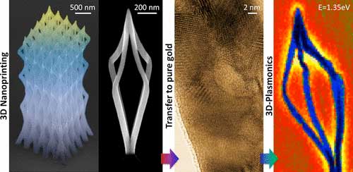
Focused electron beams are used to convert surface-bound molecules made from gold and carbon into the gas phase and deposit them to construct precise 3-D freestanding structures of pure gold
Focused electron beams are used to convert surface-bound molecules made from gold and carbon into the gas phase and deposit them to construct precise 3-D freestanding structures of pure gold. The ultra-sharp features produce free electron oscillations, or quasiparticles called plasmons, with high efficiency. (© ACS)
In a patterned sequence, researchers used a focused electron beam to dissociate surface-bound carbon- and metal-containing molecules and deposit them with precision. The result is a 3-D gold-carbon shape (shown here in a style reminiscent of Gandalf’s staff). They purified these structures in situ (inside the growth reactor) to remove carbon. They tested the resulting freestanding pure-gold architectures for plasmonic behavior—tiny, rapid waves of electron density created when light hits metal.
The 3-D printing approach produces customized, from the bottom up, nanostructures on demand. The technology paves the way to maskless fabrication of custom 1-, 2-, and 3-D architectures on virtually any material and surface shape. The materials can have specific plasmonic behaviors. Plasmonic oscillations encode more data than possible with conventional technologies. Thus, this advance may speed the advent of novel light sources, sensor devices and ultra-dense information storage technologies.
Structures on the scale of nanometers—much smaller than wavelengths of light—may improve transmission of plasmons, or small waves of electron density created when light hits an electron conductor, such as a metal.
To 3-D print nanoscale shapes with controlled properties, researchers integrated design, simulation and experiment. They used pattern sequencing to guide focused electron beams in inducing deposition of organometallic precursor molecules on a surface. Then, they removed residual carbon via in situ purification with water vapor to produce purely metallic freestanding 3-D nanostructures—an advance over previous 2-D nanoprinting with materials that contained significant carbon in addition to the desired metal. The structure that was produced—akin to the outline of up- and down-facing pyramids connected at their bases—demonstrated high plasmonic resonance at branches and tips.
On-demand 3-D printing can take place on virtually any material and surface shape, pushing nanoscale optical, mechanical, magnetic and even multifunctional materials beyond current limits and paving the way to functional plasmonic architectures for next-generation photonic, photovoltaic and data-storage technologies.
Source: Department of Energy, Office of Science

Nanoparticulele metalice vor ajuta la determinarea procentului de compuși volatili(Metallic nanoparticles will help to determine the percentage of volatile compounds)

Chimiștii ruși au inventat o tehnică care combină detecția optică utilizând benzi de testare pe hârtie cu nanoparticule triunghiulare de argint distribuite peste ele și extracție dinamică de gaze (extracția unui compus dintr-o soluție sau un amestec uscat prin intermediul gazelor lichefiate). Perspectivele acestei tehnici au fost demonstrate prin detectarea clorului. Clorul este adesea folosit pentru purificarea apei, deoarece distruge coaja exterioară a bacteriilor și a virușilor. Cu toate acestea, problema determinării concentrației de clor în apă rămâne relevantă, deoarece tehnicile existente nu sunt suficient de sensibile.

Posted: Oct 20, 2017

Metallic nanoparticles will help to determine the percentage of volatile compounds

(Nanowerk News) Researchers from the Faculties of Chemistry and of Materials Science of Lomonosov Moscow State University have developed a new way of increasing the sensitivity of detecting volatile compounds, especially chlorine, using metallic nanoparticles. The work has been published in the Talanta journal („Towards highly selective detection using metal nanoparticles: A case of silver triangular nanoplates and chlorine”).

TEM Micrograph of Aqueous Solution of Silver Triangular Nanoplates
This is an image of TEM micrograph of aqueous solution of silver triangular nanoplates. (Image: Aleksei Furletov)
Metallic nanoparticles, in particular the nanoparticles of gold and silver, are widely used in analytical chemistry. Amongst their uses is creating optical sensors based on the surface plasmonic resonance (the phenomenon of surface plasmon excitation by light) in colloidal solutions and on solid supports. Modern optical sensors have considerable advantages like high sensitivity, ease of detecting an analytic signal and adjustability of the optical and laboratory analysis parameters. Nevertheless, these devices have certain limitations when it comes to selectivity.
It happens because of aggregative instability of nanoparticles (the particles stick together when collide) which starts to happen during high ionic strength (high intensity of the electric field created by ions). The ion layer formed on the surface of particles is called the double electric layer and is characterized by an electrokinetic potential, also known as the zeta potential. With a decrease in the zeta potential, the electrostatic stabilization of nanoparticles does not happen.
The problem can be solved if the nanoparticles are attached to solid supports; scientists then acquire micro- or nanosensors based on solid particles. There are not many matrix materials for these sensors, and the process of attaching the nanoparticles to supports is not a simple one, so the researchers started working on a problem of modifying the surface of sensor matrices. For that goal they proposed separating the nanoparticles from ions and chemical compounds while retaining their sensitivity.
The Russian chemists invented a technique that combines optical detection using paper test strips with triangular silver nanoparticles spread over them, and dynamic gas extraction (the extraction of a compound from a solution or a dry mixture by means of liquefied gases). Perspectives of this technique were shown by detecting chlorine. Chlorine is often used to purify water, since it destroys the outer shell of bacteria and viruses. Nevertheless, the problem of determining the chlorine concentration in water remains relevant, since the existing techniques are not sensitive enough.
Aleksei Furletov, student of the Department of Analytic Chemistry, Faculty of Chemistry, Lomonosov Moscow State University, one of the paper’s authors, says: „The technique developed allows to determine small amounts of gaseous chlorine in the presence of large concentrations of foreign compounds without any sample preparation. This approach can be applied to other analytical systems based on metal nanoparticles, which opens up broad opportunities for the further development of this area of chemical analysis. „
Source: Lomonosov Moscow State University

Noile nano-panglici graphene conferă senzorilor o sensibilitate fără precedent(New graphene nano-ribbons lend sensors unprecedented sensitivity)

Pinning panglici de carbon de dimensiuni de ADN la un senzor de gaz poate spori sensibilitatea sale mult mai bine decat orice alt material cunoscut de carbon, spune un nou studiu de la Universitatea din Nebraska-Lincoln.
Echipa a dezvoltat o nouă formă de nano-panglică realizată din grafen, o fagure de 2-D de atomi de carbon. Atunci când cercetătorii au integrat un film al nano-panglicilor în circuitul unui senzor de gaz, acesta a răspuns de aproximativ 100 de ori mai sensibil la molecule decât au făcut senzorii cu cele mai performante materiale pe bază de carbon.

Posted: Oct 20, 2017

New graphene nano-ribbons lend sensors unprecedented sensitivity

(Nanowerk News) Pinning DNA-sized ribbons of carbon to a gas sensor can boost its sensitivity far better than any other known carbon material, says a new study from the University of Nebraska-Lincoln.

The team developed a new form of nano-ribbon made from graphene, a 2-D honeycomb of carbon atoms. When the researchers integrated a film of the nano-ribbons into the circuitry of a gas sensor, it responded about 100 times more sensitively to molecules than did sensors featuring even the best-performing carbon-based materials.
“We previously studied sensors based on other carbon-based materials such as graphene and graphene oxide,” said Alexander Sinitskii, associate professor of chemistry at Nebraska. “In the case of graphene nano-ribbons, we were certain that we would see some sensor response, but we did not expect that it would be that much higher than anything we have seen in the past.”
Reporting their findings in the journal Nature Communications („Laterally extended atomically precise graphene nanoribbons with improved electrical conductivity for efficient gas sensing”), the researchers showed that gas molecules can dramatically alter the electrical resistance of nano-ribbon films. Different gases produced varying resistance signatures, allowing the sensor to distinguish among them.
gas molecules widening the gaps between rows of graphene nano-ribbons
This rendering shows gas molecules widening the gaps between rows of the team’s graphene nano-ribbons. Nebraska’s Alexander Sinitskii and his colleagues have proposed that this phenomenon partly explains how the nano-ribbons grant sensors an unprecedented boost in sensitivity. (© Nature)
“With multiple sensors on a chip, we were able to demonstrate that we can differentiate between molecules that have nearly the same chemical nature,” said Sinitskii, a member of the Nebraska Center for Materials and Nanoscience. “For example, we can tell methanol and ethanol apart. So these sensors based on graphene nano-ribbons can be not only sensitive but also selective.”
Sinitskii and his colleagues suspect that the nano-ribbons’ remarkable performance stems partly from an unusual interaction between the ribbons and gas molecules. Unlike its predecessors, the team’s nano-ribbons — which resemble ordered rows of Charlie Brown’s shirt stripes — stand vertically rather than lying flat on a surface. The team has proposed that gas molecules can nudge these rows apart, effectively lengthening the gaps between nano-ribbons that electrons must jump to conduct electricity.

Enter the (benzene) ring

Graphene, whose 2004 discovery eventually earned a Nobel Prize, boasts unmatched electrical conductivity. But the material’s lack of a band gap — which requires electrons to gain energy before jumping from their near orbits around atoms to an outer “conduction band” that drives conductivity — initially prevented researchers from switching off that conductivity. This, in turn, posed challenges to applying graphene in electronics that require adjusting the material’s conductivity at will.
One potential solution involved trimming sheets of graphene down to nanoscopic ribbons that computer simulations suggested would possess the elusive band gap. This proved difficult to do with the atomic precision needed to preserve the properties that made graphene appealing in the first place, so researchers began fabricating ribbons from the bottom up by strategically snapping together molecules on certain types of solid surfaces. Though the process worked – and the resulting ribbons did have a band gap – it limited researchers to fabricating just a few ribbons at a time.
In 2014, Sinitskii pioneered an approach that could mass-produce nano-ribbons in a liquid solution, a vital step toward scaling up the technology for electronic applications. But the films made from these nano-ribbons were not conductive enough to perform electrical measurements. The team’s newest study adapted the original chemical approach by adding benzene rings — circular molecules with six atoms of both carbon and hydrogen — onto either side of a first-generation nano-ribbon. These rings widened the ribbon, reducing its band gap and enhancing its ability to conduct electricity.
“People do not often think of graphene nano-ribbons as a sensor material,” Sinitskii said. “However, the same (property) that makes the nano-ribbons good for devices such as transistors – the ability to change their conductivity by several orders of magnitude — is also what makes them good for sensors.
“It is possible to design many different kinds of graphene nano-ribbons with very diverse properties. Only a few types have been experimentally demonstrated so far, but there are many interesting theoretical predications about ribbons that are yet to be synthesized by chemists. So it is very likely that new nano-ribbons with even better sensor characteristics or other exciting properties will be developed in the near future.”
Source: By Scott Schrage, University of Nebraska-Lincoln

Oamenii de știință revizuiesc constantele optice ale filmelor de aur ultrascurte(Scientists revisit optical constants of ultrathin gold films)

Filmele metalice cu o grosime de zeci de nanometri sau zeci de miliarde de metru sunt utilizate pe scară largă pentru a produce senzori compacți chimici și biologici, fotodetectoare, celule solare și componente pentru computere optice. Atunci când nanofilmele sunt mai subțiri decât 10 nanometri, ele devin nu doar conductive, ci și flexibile și transparente, care ar putea fi aplicabile într-o varietate de dispozitive moderne.Astfel de filme pot fi folosite în optică și optoelectronică pentru a dezvolta biosenzori compacți cu sensibilitate ridicată, celule solare, fotodetectoare în bandă largă și componente computerizate optoelectronice”. Filmele de aur de acest tip, cu o grosime de aproximativ 40 nanometri, sunt deja utilizate în proiectarea biosenzorilor.

Posted: Oct 17, 2017

Scientists revisit optical constants of ultrathin gold films

(Nanowerk News) Researchers at Moscow Institute of Physics and Technology (MIPT) have conducted highly precise measurements of the optical constants of ultrathin gold films with thicknesses ranging from 20 to 200 billionths of a meter in the optical part of the electromagnetic spectrum. Thin gold films are key components of modern micro- and nanoscale optical and optoelectronic devices. The research findings will be in demand among researchers in the field. The paper was published in the journal Optics Express („Optical constants and structural properties of thin gold films”).

Metal films with a thickness of tens of nanometers, or tens of billionths of a meter, are widely used to produce compact chemical and biological sensors, photodetectors, solar cells, and components for optical computers. When nanofilms are made thinner than 10 nanometers, they become not just conductive but also flexible and transparent, which might be applicable in a variety of modern devices.
gold thin-film
Preparation of a thin gold film sample for spectroscopic ellipsometry measurements. (Image: MIPT)
Gold, which is widely used in nanoscale device development, has proved to be the most suitable metal for the purpose. Such applications require gold in the form of very thin films or nanostructures. To develop and optimize devices, precise data on the properties of such films are necessary. But most of the data used by researchers at present are reported in papers published almost half a century ago.
For instance, one of the most frequently cited articles on the optical constants of gold is „Optical constants of the noble metals” by P.B. Johnson and R.W. Christy, published as early as 1972. The Scopus citation database reveals that the reference constants for gold from this paper have been used in at least 10,000 other publications. To appreciate the significance of this work, it is important to keep in mind that in the 70s, research into the optical properties of thin metal films required a tremendous effort, because the challenging experiments had to be followed by complex calculations and computers were not yet widespread.

Thinner is better

State-of-the-art laboratory equipment and the nearly unlimited computing power available to modern researchers enable more detailed studies of thin metal films. However, it is known that the optical properties of such films – and therefore the efficiency of devices based on them – depend on factors such as film thickness, deposition rate, and the temperature of the substrate used for film deposition.
Accordingly, the MIPT researchers adjusted the initial conditions, namely the deposition rate and the substrate temperature, so as to optimize the optical properties of the film. After that, they conducted the necessary measurements by means of spectroscopic ellipsometry, X-ray diffractometry, electron and atomic force microscopy. The data obtained allowed the MIPT team to study in detail how the properties of thin gold films are related to their structure and average grain size.
The structure of a material affects its physical properties to a large extent, because it is at grain boundaries that conduction electrons are scattered, losing energy – the way a ball in a pinball machine loses its momentum as it runs into obstacles. As it turned out, both optical losses and direct current resistivity are substantially increased, as the thickness of the gold film is reduced to below 80 nanometers.
The authors of the paper provide reference data on the optical constants of gold for a wide range of wavelengths, from 300 to 2,000 nanometers, for films that are 20 to 200 nanometers thick. These findings will be of use to researchers working on various nanophotonic devices and metamaterials.

State-of-the-art technology

To grow thin films, the researchers used a technique called electron beam evaporation, which involves the following steps:: A purified silicon substrate is introduced into a vacuum chamber. Opposite the substrate, a metal sample is positioned. The metal, in this case gold, is then subjected to a beam of electrons accelerated by an electric field. This rapidly heats up the gold causing it to melt and eventually transform into vapor. The evaporated gold atoms are then transported across a region of low pressure from their source and undergo condensation on the substrate to form the thin film.
„Provided that you maintain a high vacuum, heat the metal appropriately, and otherwise follow the procedure, this technique yields films of arbitrary thickness, which is determined by the evaporation time. Moreover, the films are almost perfectly smooth, having a roughness of less than a nanometer,” comments Valentyn Volkov, who heads the Laboratory of Nanooptics and Plasmonics at MIPT. „Such films can be used in optics and optoelectronics to develop high-sensitivity compact biosensors, solar cells, broadband photodetectors, and optoelectronic computer components.” Gold films of this kind with a thickness of about 40 nanometers are already used in biosensor design.
Source: Moscow Institute of Physics and Technology

Plasmonii într-o cutie deschisă creează un laser miniatural(Plasmons in an open box create miniature laser)

Simulările sugerează că laserul SPP ar putea deveni un detector și mai sensibil pentru materialele biologice, chimice și de mediu decât utilizarea doar a cavității rezonante. Designul laserului permite, de asemenea, integrarea ușoară într-un circuit fotonic și poate permite, de asemenea, noi studii ale plasmonicii cuantice, interacțiunea nanometrică a materiei cu proprietățile cuantice ale luminii.

Posted: Oct 13, 2017

Plasmons in an open box create miniature laser

(Nanowerk News) Scientists at the National Institute of Standards and Technology (NIST) have developed the first miniature laser in which the light is guided along the floor of an open metallic trench. The laser could act as a nanoscale device to sense minute amounts of pollutants and other chemicals in the environment, or detect the surface binding of biomolecules for medical diagnostics.

Wenqi Zhu of NIST and the University of Maryland, along with NIST physicists Henri Lezec and Amit Agrawal, described their work (link is external) in a recent edition of Science Advances(„Surface-Plasmon-Polariton Laser based on a Metallic Trench Fabry-Perot Resonator”). The work was performed in collaboration with Nanjing University in China and the University of Michigan.
Illustration depicts cavity and sidewalls, made of silver, that form a miniature laser
Illustration depicts cavity and sidewalls, made of silver, that form the miniature laser fabricated by scientists working at NIST. The cavity’s ultrathin coating (flat red layer) is the amplifying layer used to induce SPP lasing under illumination from above (blue-green light beam); a small amount of the red laser light leaks through a nanoscale notch positioned just below the cavity’s floor enabling researchers to monitor small wavelength shifts induced by the presence of the molecules on the cavity floor. (Image: NIST)
The development of the new laser relies on the interaction between photons—particles of light—and the sea of electrons that floats along the surface of a metal. Interactions between the photons and ripples in the electron sea yield a special type of light wave, dubbed a surface plasmon polariton (SPP), which is tightly confined to travel only along the metal’s surface. This confinement makes the SPPs highly sensitive to anything lying on the metal surface.
As a first step toward building the miniature laser, the team fashioned out of silver a small trench-shaped open cavity in which SPPs can resonate. The cavity is a flat surface flanked by tiny, mirror-like sidewalls that reflect the surface waves back and forth.
Through careful fabrication, the resonant cavity possessed two key properties: all of its interior surfaces were smooth on an atomic scale, varying in thickness by no more than a few nanometers, and its sidewalls were perpendicular with respect to the flat cavity floor. The design, made possible by molding silver using a precisely patterned silicon template, enabled the SPPs to bounce back and forth across the cavity hundreds of times without losing significant energy, like a guitar string sustaining a pure note for a long time. That property, known as high quality factor, or high Q, is essential for constructing a laser. The Q measured by the team is the highest to date for any visible-light resonator using only SPPs.
The high Q also enabled the cavity to act as an extremely selective filter for SPPs—only those with wavelengths that fell within a narrow band could resonate in the cavity. The narrow range is important because it enables the resonant cavity (even before it became part of a laser) to become a highly sensitive detector of tiny changes in its environment—the presence of particulate matter or the addition of a thin film to the cavity’s floor. Such changes shift the center of the band of wavelengths that will resonate in the cavity.
“By achieving a narrow resonance, the shift in wavelength is clear, and the open cavity can act as an exquisitely sensitive detector,” said Lezec.
After demonstrating that the cavity could be used as a sensor, the team then worked to turn their design into a laser. They did so by adding an ultrathin coating to the cavity that amplified the intensity of the SPP traveling through the structure. This is the first nanoscale laser ever constructed by manipulating an SPP traveling on a single flat metal surface, Lezec noted.
Simulations suggest the SPP laser could become an even more sensitive detector for biological, chemical and environmental materials than using just the resonant cavity. The design of the laser also enables it to be easily integrated into a photonic circuit and may also enable new studies of quantum plasmonics, the nanoscale interaction of matter with the quantum properties of light.
Source: NIST

Senzor de hidrogen ultra-rapid și ultra-sensibil pentru nanofire(Ultra-fast and ultra-sensitive nanowire hydrogen sensor)

O echipă KAIST a realizat un senzor de hidrogen ultra rapid care poate detecta nivelurile de gaze de hidrogen sub 1% în mai puțin de șapte secunde. De asemenea, senzorul poate detecta sute de părți la un milion de niveluri de hidrogen gazos în 60 de secunde la temperatura camerei ( materiale și interfețe aplicate ACS , „Nanowires compozit Pd-Ag compozit pentru răspuns rapid și senzori de hidrogen transparent” ).Profesorul Kim se așteaptă ca senzorul ultra-rapid de hidrogen să poată fi util pentru prevenirea accidentelor de explozie provocate de scurgeri de hidrogen gazos. În plus, se așteaptă ca alte gaze nocive din aer să poată fi detectate cu precizie prin nano-filtrare eficientă prin utilizarea unei varietăți de straturi MOF.

Posted: Sep 29, 2017

Ultra-fast and ultra-sensitive nanowire hydrogen sensor

(Nanowerk News) A KAIST team made an ultra-fast hydrogen sensor that can detect hydrogen gas levels under 1% in less than seven seconds. The sensor also can detect hundreds of parts per million levels of hydrogen gas within 60 seconds at room temperature (ACS Applied Materials and Interfaces, „Hollow Pd-Ag Composite Nanowires for Fast Responding and Transparent Hydrogen Sensors „).

A research group under Professor Il-Doo Kim in the Department of Materials Science and Engineering at KAIST, in collaboration with Professor Reginald M. Penner of the University of California-Irvine, has developed an ultra-fast hydrogen gas detection system based on a palladium (Pd) nanowire array coated with a metal-organic framework (MOF).
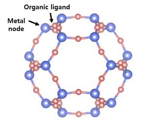
text
Schematic illustration of a metal-organic framework (MOF). The MOF, consisting of metal ions and organic ligands, is a highly porous material with a ultrahigh surface area. The various structures of MOFs can be synthesized depending on the kinds of metal ions and organic ligands. (Image: KAIST)
Hydrogen has been regarded as an eco-friendly next-generation energy source. However, it is a flammable gas that can explode even with a small spark. For safety, the lower explosion limit for hydrogen gas is 4 vol% so sensors should be able to detect the colorless and odorless hydrogen molecule quickly.
The importance of sensors capable of rapidly detecting colorless and odorless hydrogen gas has been emphasized in recent guidelines issued by the U.S. Department of Energy. According to the guidelines, hydrogen sensors should detect 1 vol% of hydrogen in air in less than 60 seconds for adequate response and recovery times.
Ultra-fast and ultra-sensitive nanowire hydrogen sensor
Representative image of this paper published in ACS Nano on Sept. 26.
To overcome the limitations of Pd-based hydrogen sensors, the research team introduced a MOF layer on top of a Pd nanowire array. Lithographically patterned Pd nanowires were simply overcoated with a Zn-based zeolite imidazole framework (ZIF-8) layer composed of Zn ions and organic ligands. ZIF-8 film is easily coated on Pd nanowires by simple dipping (for 2-6 hours) in a methanol solution including Zn (NO3)2·6H2O and 2-methylimidazole.
As synthesized ZIF-8 is a highly porous material composed of a number of micro-pores of 0.34 nm and 1.16 nm, hydrogen gas with a kinetic diameter of 0.289 nm can easily penetrate inside the ZIF-8 membrane, while large molecules (>0.34 nm) are effectively screened by the MOF filter.
Thus, the ZIF-8 filter on the Pd nanowires allows the predominant penetration of hydrogen molecules, leading to the acceleration of Pd-based H2 sensors with a 20-fold faster recovery and response speed compared to pristine Pd nanowires at room temperature.
Images of Pd nanowire array-based hydrogen sensors, scanning electron microscopy image of a Pd nanowire covered by a metal-organic framework layer, and the hydrogen sensing properties of the sensors
Images of Pd nanowire array-based hydrogen sensors, scanning electron microscopy image of a Pd nanowire covered by a metal-organic framework layer, and the hydrogen sensing properties of the sensors. (Image: KAIST)
Professor Kim expects that the ultra-fast hydrogen sensor can be useful for the prevention of explosion accidents caused by the leakage of hydrogen gas. In addition, he expects that other harmful gases in the air can be accurately detected through effective nano-filtration by using of a variety of MOF layers.
Source: The Korea Advanced Institute of Science and Technology (KAIST)

Digitizatoarele cu infraroșu cu putere zero, bazate pe microprocesoare micromecanice îmbunătățite cu plasmă(Zero-power infrared digitizers based on plasmonically enhanced micromechanical photoswitches)

Senzorii de ultimă oră folosesc electronica activă pentru a detecta și a discrimina vibrațiile, vibrațiile sonore și alte semnale

Infrared-analytical pag 35-47