Nanocars luate pentru o plimbare dur(Nanocars taken for a rough ride)

au constatat în testele recente că conducerea autovehiculelor lor în condiții ambientale expuse la aer liber, mai degrabă decât un vid – a pierdut după o vreme, deoarece mașinile hidrofobe cu o singură moleculă au rămas pe drum și au creat ceea ce sa ridicat la lovituri de viteză mari.Cercetătorii au remarcat că nu puteau vedea noile modele cu microscoape de scanare pentru că aceștia lucrează doar în vid și emit energie care ar putea influența circulația autovehiculelor

Nanocars

Printr-un pahar, cald: Nanomaterialele pot ajuta la eficientizarea ferestrelor

Nanofoamul care se dezvoltă – cunoscut sub numele de compozit nanocelular cu izolație termică superioară și izolare fonică – utilizează bule de gaz mai mici de 100 nanometri în diametru pentru a bloca transferul de căldură și sunet prin ferestrele de sticlă, permițând lumina vizibilă să treacă și să mențină o claritate Similar cu ferestrele normale

Posted: Jun 01, 2016

Through a glass, warmly: Nanomaterials can help make windows more efficient

(Nanowerk News) A team of researchers at the U.S. Department of Energy’s (DOE’s) Argonne National Laboratory is using nanomaterials to improve the energy efficiency of existing single-pane windows in commercial and residential buildings. The team was recently awarded a $3.1 million grant from DOE’s Advanced Research Projects Agency-Energy (ARPA-E) to develop a technology that could help achieve that goal. The nanofoam the team is developing – known as a nanocellular composite with super thermal insulation and soundproofing – uses gas bubbles less than 100 nanometers in diameter to block the transfer of heat and sound through glass windows while allowing visible light to pass through and maintain a clarity similar to normal windows.

chemical engineer Jie Li, left, and postdoctoral researcher Alina Yan create coated nanoparticles in a continuous flow reactor
Principal chemical engineer Jie Li, left, and postdoctoral researcher Alina Yan create coated nanoparticles in a continuous flow reactor. Nanoparticles are key to an ongoing effort at Argonne to create more efficient window films.
“That’s really the trick, blocking the heat and sound transfer while maintaining transparency,” said Ralph Muehleisen, principal building scientist at Argonne. “It’s fairly simple to develop a coating that insulates, but getting one that is thin and you can still see through is a substantial technical challenge.”
The nanofoam, which will be extruded into sheets about three millimeters thick, creates a thermal insulation effect by using the tiny bubbles to reduce collisions among gas molecules, thereby reducing the transfer of heat energy. When the bubbles are reduced to that scale, super thermal insulation becomes possible.
A foam with larger bubbles could perform a similar function, but those bubbles would scatter visible light, making the window hazy and less transparent. The bubbles need to be created with a size of around 100 nanometers or less, distributed properly and then sculpted within the host medium to achieve an acceptable level of clarity.. By way of comparison, a human hair is about 60,000 nanometers wide and a DNA molecule is 2-3 nanometers wide.
According to ARPA-E, single-pane windows make up 30-40 percent of windows in the United States, depending on the region. Single-pane windows conduct at least twice as much heat as double paned, so retrofitting all those windows could save consumers about $12 billion a year in energy costs.
The nanofoam team combines expertise from nanomaterial scientists, polymer scientists, chemical, process and building engineers, along with the expertise of Argonne’s Center for Nanoscale Materials, a DOE Office of Science user facility. The team also includes researchers from the University of Chicago’s Institute for Molecular Engineering, Lawrence Berkeley National Laboratory (LBNL) and Temple University’s Department of Chemistry.
“This effort really shows the power of cross-cutting scientific collaboration,” said Matt Tirrell, who is Argonne’s Deputy Laboratory Director for Science and holds a joint appointment with the University of Chicago. “By bringing together these unique skillsets and facilities, we have the ability to make substantial breakthroughs that hold the promise to make a big difference in building energy efficiency.”
The team will not be satisfied with creating laboratory versions of the materials, however. Researchers are also developing processes that can be economically scaled up to commercial production. Jie Li, a principal chemical engineer at Argonne and the principal investigator on the project, recently completed the DOE’s Lab-Corps program, which aims to accelerate the transfer of clean energy technologies from national laboratories to the marketplace.
“We know that commercial production is the key step to having a positive effect on building efficiency,” Li said. “There are billions of square feet of windows in the US. Imagine the impact of making all those windows more efficient. That’s when you really start to see benefit from your science.”
The team also includes Leah Guzowski, director of strategic programs at Argonne, Yugang Sun, formerly of Argonne and now a professor at Temple University, and Stephen Selkowitz and Charlie Curcija from the Windows and Daylighting Group at LBNL.
This nanofoam research builds upon another nanomaterial being developed at Argonne. Several members of the ARPA-E team are working on a new nanoparticle coating of vanadium dioxide, which is a phase-change material that behaves differently at different temperatures. At low temperatures, vanadium dioxide is a semiconductor that allows both near-infrared light (the portion of the solar spectrum that contains approximately half of all solar energy) and visible light to pass through. When it gets hot, however, it develops metallic properties and begins to block out near-infrared light, which helps reflect solar radiation during the summer. Current versions of vanadium dioxide do not block much solar heat gain, so the film must be very thick, which makes for a darker window that consumers are reluctant to adopt.
By using nanoparticles of vanadium dioxide, the team has created a film that can boost near-infrared blocking and is more efficient at reflecting solar radiation, all while maintaining visible transparency.
The Argonne researchers hope that by combining the nanofoam and the vanadium dioxide, they may be able to create a single-pane window that could achieve efficiencies similar to multi-pane Low-E units. Low-E windows usually have multiple coated panes of glass with inert gas suspended between them. By using only one pane of glass without the costly and complicated sealing system required by multi-paned windows, the new windows would become more affordable, allowing more widespread adoption.
Source: Argonne National Laboratory

Read more: Through a glass, warmly: Nanomaterials can help make windows more efficient

Undă moleculară a catalizatorului pe bază de oxid de metal nanosizat

Studiul recent al grupului Ananikov a vizat formarea legăturii carbon-heteroatom catalizată de oxizii de cupru de dimensiuni nano. Acest tip de reacție catalitică interesantă utilizează nanoparticule CuO și Cu2O pentru a promova transformările chimice. Studiul mecanic a relevat o imagine destul de complicată a evoluției catalizatorului. În reacția C-S de cuplare încrucișată, oxidul de cupru cu dimensiunea nano a fost transformat în specii metalice solubile: tiolații de cupru [Cu (SR) n] s-au format ușor în reacția oxidului de cupru cu tioli (RSH). Într-adevăr, procesul studiat demonstrează că reacția presupusă în mod tradițional pe suprafața oxidului de metal nu aduce o contribuție primară la formarea produsului. Modificarea oxidului metalic și transferul de soluții corespunzătoare de tiolat de metal în soluție au fost responsabile de formarea formei active a catalizatorului.
În ciuda căii catalitice eterogene așteptate, studiul reacției de cuplare încrucișată a evidențiat solubilizarea oxidului de cupru și a catalizei omogene de stare a soluției. Mișcarea complecșilor de cupru la soluție a fost însoțită de eliberarea apei: Cu2O + 2RSH = 2CuSR + H2O

Posted: Jun 01, 2016

Molecular wave of nanosized metal oxide catalyst

(Nanowerk News) Metal oxides represent primary source of catalytic materials for a variety of industrial and research applications, either as an active phase or as a supporting phase. Mechanistic studies conducted by Ananikov group revealed formation of catalytically active species due to partial dissolution of metal oxide in the reaction mixture and generation of soluble metal complexes (ACS Catalysis, „Nature of the Copper-Oxide-Mediated C–S Cross-Coupling Reaction: Leaching of Catalytically Active Species from the Metal Oxide Surface”). Therefore, metal oxides are not directly involved in heterogeneous catalysis; rather, they can be considered as a source of reactive species for solution-state homogeneous catalysis (DOI: 10.1021/acscatal.6b00337).

Catalysis is the major driving force in modern industry. Catalysis is vital in production of fuels, materials, drugs, and a variety of molecular and composite chemicals. Around 80% of all industrial processes involve catalytically produced components or catalytic technologies. Metal oxides represent a traditional class of solid materials to create active phases of catalysts or to construct supports for other types of active centers. Metal oxides as active phases are designed to render chemical transformation and directly participate in the catalytic cycle. Metal oxides as supporting phases are used to introduce innocent component with high stability.
Cryogenic scanning electron microscopy study of solution phase of catalytic cross-coupling reaction
Cryogenic scanning electron microscopy study of solution phase of catalytic cross-coupling reaction. (Image: Ananikov group)
Recent study of Ananikov group addressed carbon-heteroatom bond formation catalyzed by nano-sized copper oxides. This intriguing type of catalytic reactions utilizes CuO and Cu2O nanoparticles to promote chemical transformations. Mechanistic study revealed rather complicated picture of catalyst evolution. In C-S cross-coupling reaction, nano-sized copper oxide was transformed to soluble metal species: copper thiolates [Cu(SR)n] were readily formed in the reaction of copper oxide with thiols (RSH). Indeed, the studied process demonstrates that traditionally assumed reaction on the surface of metal oxide do not make a primary contribution to the product formation. Modification of metal oxide and transfer of corresponding metal thiolate species to solution were responsible for the formation of active form of the catalyst.
Despite expected heterogeneous catalytic pathway, the study of cross-coupling reaction revealed solubilization of copper oxide and solution state homogeneous catalysis. Movement of copper complexes to solution was accompanied by release of water: Cu2O + 2RSH = 2CuSR + H2O. Cryogenic scanning electron microscopy suggested formation of a complex catalytic system with substantial evolution of initial form of metal oxide during the catalytic reaction (see Figure).
The occurred transformations may change the paradigm of metal-oxide-based systems application in catalysis for both options – active phase and supporting phase. In the former option, if metal oxide is assumed as an active phase, transition to solution drastically changes the nature of the catalytic process. In the latter option, if metal oxide is utilized as a support, the oxide does not behave as an innocent material and cannot be recovered in the original state.
Catalyst stability and recycling are the key properties affected by the reported transformation of the metal oxide. Knowledge of mechanistic nature of catalyst evolution opens up new possibilities to reduce cost of chemicals production processes.
Source: Zelinsky Institute of Organic Chemistry
Subscribe to a free copy of one of our daily
Nanowerk Newsletter Email Digests
with a compilation of all of the day’s news.

Read more: Molecular wave of nanosized metal oxide catalyst

Nanoparticule pentru înlocuirea elementelor de pământuri rare în magneți permanenți

Cercetatorii au folosit un complex mixt de oleat de cobalt-cobalt intr-o abordare sintetica intr-un singur pas pentru a produce nanoparticule magnetice core-shell. Materialele rezultate au prezentat proprietăți magnetice puternice și capacități de stocare a energiei.

Posted: Jun 01, 2016

Nanoparticles to replace rare-earth elements in permanent magnets

(Nanowerk News) Technologies from wind turbines to electric vehicles rely on critical materials called rare-earth elements. These elements, though often abundant, can be difficult and increasingly costly to come by.

Now, scientists looking for alternatives have reported in ACS’ journal Chemistry of Materials („Strongly exchange coupled core|shell nanoparticles with high magnetic anisotropy: a strategy towards Rare Earth -free permanent magnets”) a new way to make nanoparticles that could replace some rare-earth materials and help ensure the continued supply of products people have come to depend on.
Rare-earth elements have unique characteristics that make them very useful. For example, the world’s strongest magnets are made with neodymium. A little too powerful for your refrigerator, these magnets are incorporated into computer disk drives, power windows and wind turbines.
But rare earths are challenging to mine and process, and prices can rise quickly in a short period of time. Given the increasing demand for rare earths, Alberto López-Ortega, Claudio Sangregorio and colleagues set out to find substitutes for use in strong magnets.
The researchers used a mixed iron-cobalt oleate complex in a one-step synthetic approach to produce magnetic core-shell nanoparticles. The resulting materials showed strong magnetic properties and energy-storing capabilities.
Their approach could signal an efficient new strategy toward replacing rare earths in permanent magnets and keeping costs stable, the researchers say.
Source: American Chemical Society

Read more: Nanoparticles to replace rare-earth elements in permanent magnets

Atomii -materiale cuantice topologice

clase de materiale complet noi, cunoscut sub numele de „materiale cuantice topologice^

Posted: May 31, 2016

Atome mit dem gewissen Twist

(Nanowerk News) Gewisse Materialien wie Metalle leiten den Strom, andere, sogenannte Isolatoren wie Glas oder Keramik nicht. Nun ist es Forschern der Universität Hamburg erstmals gelungen, die zentrale Kenngröße einer Klasse ganz neuer Materialien, der sogenannten „topologischen Quantenmaterialien“ zu vermessen. Von diesem speziellen „Twist“, einer trickreichen Verdrehung der Wege der Elektronen, hängen zum Beispiel die Leitfähigkeit und andere Eigenschaften ab.

Die Ergebnisse eröffnen ganz neue Perspektiven für die Entwicklung neuer Quantenmaterialien, auch mit potenziellen Anwendungen bei zukünftigen Quantencomputern. Sie wurden nun im Fachmagazin Science veröffentlicht („Experimental reconstruction of the Berry curvature in a Floquet Bloch band”).
Geometrie der Eigenstände zweier Bloch-Bänder
Künstlerische Darstellung der berechneten Geometrie der Eigenstände der zwei Bloch-Bänder. (Bild: UHH/Sengstock)
In üblichen Materialien müssen sich Elektronen, die für den Stromtransport verantwortlich sind, ihren Weg durch gleichmäßig verteilte Hindernisse im Festkörper bahnen. In den topologischen Quantenmaterialien können sich Teilchen dagegen nur auf gewissen, mehr oder weniger verdrehten Wegen (die einen Twist beinhalten) bewegen und verhalten sich entsprechend den Gesetzen der Quantenphysik zudem wie Teilchen und Wellen gleichzeitig.
Es gibt eine zentrale Eigenschaft, die die Topologie, also den Quanten-Twist dieser Materialien, komplett beschreiben kann: die „Berry Krümmung“, benannt nach dem englischen Physiker Michael Berry, der das Grundkonzept dazu bereits in den 1980er Jahren angelegt hat. Das Team um Prof. Dr. Klaus Sengstock und Dr. Christof Weitenberg vom Institut für Laserphysik der Universität Hamburg konnte die Berry Krümmung in einem Quantenmaterial nun erstmalig vollständig vermessen.
Die Physiker nutzten bewusst ein künstliches Quantenmaterial, das heute weltweit intensiv eingesetzt wird: atomare Wolken – sogenannte „ultrakalte Quantengase“ – in einem künstlichen Festkörper, gebildet aus Laserlicht. Nachdem die Atome, die in diesen Experimenten die Rolle von Elektronen in Festkörpern übernahmen, in das künstliche Material, das die zu untersuchende Topologie enthielt, eingebracht worden waren, konnte mithilfe weiterer Laser diese Topologie sehr präzise gemessen werden.
Dr. Weitenberg, der die Experimente betreute, betont: „Wir konnten bereits in diesen ersten Experimenten die Topologie eines künstlichen Materials bestimmen, und das ist erst der Anfang, wir alle sind sehr begeistert von den Möglichkeiten dieser neuen Methode.“ Prof. Sengstock ergänzt: „Neuartige Quantenmaterialien werden schon in naher Zukunft eine wichtige Rolle in den absehbaren Quantentechnologien spielen; Quantencomputer sind dabei besonders visionär und nur durch neue Konzepte zu verwirklichen.“ Materialien mit dem gewissen Twist können vermutlich dazu wichtige Beiträge liefern: „Es ist besonders spannend, in diesem Bereich zu forschen, da das Forschungsfeld dieser neuen Quantenmaterialien erst ganz am Anfang steht, vieles ist noch gar nicht erforscht“, so Prof. Sengstock.
Source: Universität Hamburg

Read more: Atome mit dem gewissen Twist

Nanotehnologii sunt pași mici spre fabricarea atomică la scară 3D

se va deschide porțile pentru tehnologiile emergente în calcul, energie, cataliza, și o serie de alt articol de revizuire recente fields.A (în ACS Nano „Directing Materia: Spre Nanofabrication Atomic-Scale 3D „) Ilustrează utilizarea fascicule de electroni și ioni concentrat (e-grinzi și traverse) pentru a induce reacții chimice foarte localizate la interfețe solide la vapori și solid-lichid, amorfe transformări de fază cristaline cu precizie strat atomic, iar mișcarea atom specific dopant unic, în barilor de cristal, punând astfel bazele pentru asamblarea atomically precis direcționată a materialelor și a creșterii devices.

Nanotechnology’s tiny steps toward atomic-scale 3D fabrication

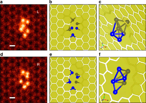
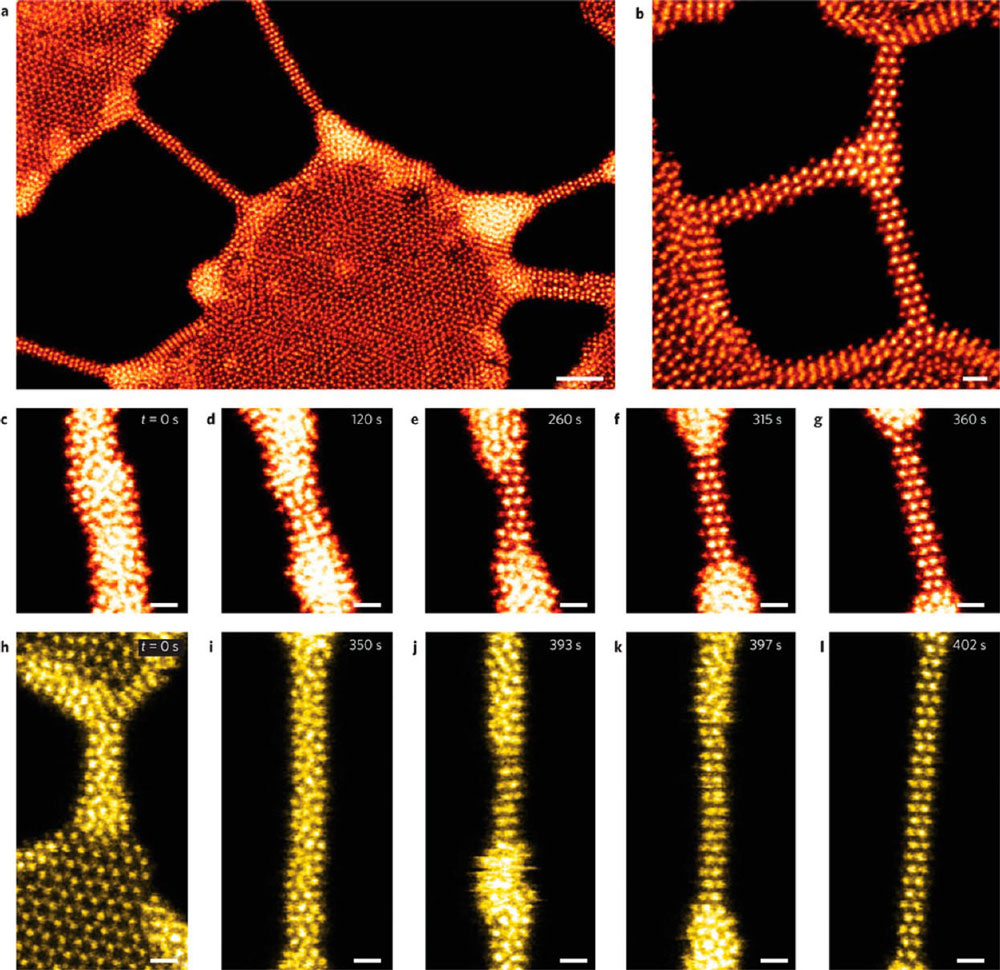
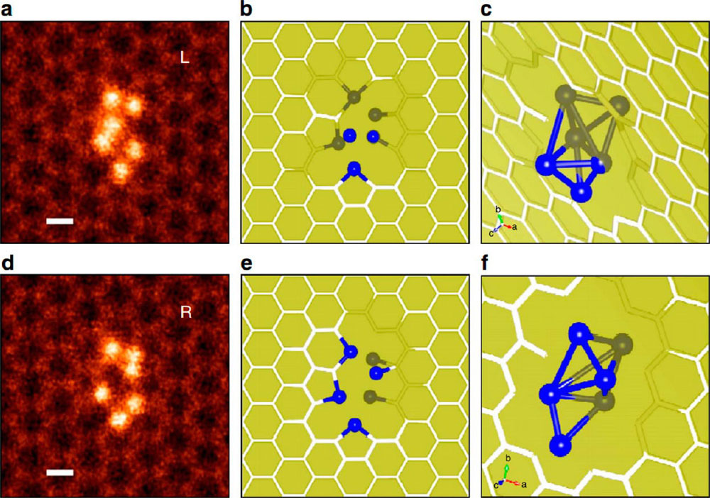
(Nanowerk Spotlight) Over the past few decades, the development of electron microscopy has gone hand in hand with techniques for atomically precise fabrication of 3D structures based on electron and ion beams.All material functionality is governed by the type, arrangement, and bonding of atoms. Enabling the capacity to perform atomically precise directed assembly of matter will open the doors to emerging technologies in computing, energy, catalysis, and a plethora of other fields.A recent review article in ACS Nano („Directing Matter: Toward Atomic-Scale 3D Nanofabrication”) illustrates the use of focused electron and ion beams (e-beams and i-beams) to induce highly localized chemical reactions at solid-vapor and solid-liquid interfaces, amorphous to crystalline phase transformations with atomic layer precision, and the motion of specific single dopant atoms within crystal lattices, thus laying the foundation for atomically precise directed assembly of materials and devices.The growth of plasmonic gold nanostructures by electron beam induced deposition (EBID) has been demonstrated already 10 years ago and the physics behind this nanofabrication technique has been explored (see for instance: „Scientists unveil new physics behind the nanofabrication technique of electron beam induced deposition„). The process has been improved over the years and researchers are now able to grow structures much faster with a broad range of precursors (see: „A new process for rapidly fabricating complex 3D nanostructures„).In their review, the authors emphasize the synergy between imaging, nanofabrication, and modeling in order to reveal the fundamental mechanisms of charged particle-surface interaction.They present several recent examples that suggest the feasibility of atomically precise fabrication in the bulk, including creating specific dopant configurations, ordered vacancy planes, and other structures.The article covers EBID/IBID from gas or liquid precursors, e-beam-induced crystallization in the bulk, and the ability to image and to analyze single atoms and defects in 2D structures.Patterning of a MoSe nanowire network(a) Patterning of a MoSe nanowire network, where each nanowire is sculpted individually. (b) Ramified Y junction made of three MoSe nanowires. (c-l) Serial snapshots of the sculpting process of individual MoSe (c-g) and MoS (h-l) nanowires. All images are STEM Z-contrast images, false-colored for better visibility. Scale bars, 2 nm (a), 0.5 nm (b-l). (© Nature Publishing Group) (click on image to enlarge)Electron-beam/ion-beam-induced deposition from gas precursorsDiscussing Focused Electron-Beam-Induced Processing – a nanoscale direct-write synthesis technique where an electron beam directs assembly of a surface-adsorbed precursor via an electron-stimulated chemical reaction – and Focused Ion-Beam-Induced Processing – where the deposition and etching of nanoscale materials is induced by a focused ion beam – the authors show how these techniques were developed; they discuss their benefits but also obstacles to large-scale implementation.Eelectron-beam/ion-beam-induced deposition from liquid precursorsAn alternative pathway to using gas precursors for direct nanofabrication is direct-write with electron and/or ion beams with a liquid precursor. This method utilizes the e-beam or i-beam as an ionizing source that decomposes solvent molecules to generate solvated electrons and other radicals in a complex cascade of reaction pathways.When using electrons to direct-write in solution, the minimal size of the created structures is limited to the nanometer scale due to the fundamental physics of the interactions between the electron beam and the liquid, including the lateral transport of solvated electrons and ionic species. The helium ion beam, on the other hand, might offer the potential for improved resolution.Atomically precise e-beam-induced crystallization in the bulkE-beam and i-beam patterning are popular and versatile approaches for creating structures on ∼10-100 nm scales, typically in SEM-like geometry. However, in the field of imaging, high-resolution transmission electron microscopy (TEM) has long been a tool of choice because it allows for atomic-scale studies of crystals and nanoparticles.As the authors note, over the last 15 years, aberration correction has pushed the achievable resolution into the sub-angstrom range and allowed for much greater localization of the probe in STEM geometry, suggesting that higher precision patterning should be achievable using these improved electron probes.Provided that the electron beam path can be programmed, localization of features in the areas illuminated by the beam and the ability to control their growth allows for more complex patterning.The team writes that the manufacturing of epitaxial crystalline nanostructures with predefined shapes is particularly interesting, as adjustable strain states could yield ways to control properties, and the ordered final structures can be more easily modeled than amorphous structures.Si6 cluster configurations embedded in a graphene pore(a,d) ADF Z-contrast images of two representative stable Si6 cluster configurations embedded in a graphene pore. (b,e) Two- and (c,f) three-dimensional structures obtained from first-principles calculations. Si and C atoms below the graphene plane are shaded. L or R labels are used to highlight when the oscillating Si atom is either at the left or right sites. Scale bar, 0.2 nm. (© Nature Publishing Group) (click on image to enlarge)Single-atom dynamics and beyondThe difficulties in manipulating single atoms for nanoscale engineering were famously highlighted by Stemmer („Three-dimensional imaging of individual dopant atoms in SrTiO3„).The use of an electron beam might provide an answer to this dilemma by allowing the direct addressing of single atoms in bulk 3D materials.The review highlights results („Direct Observation of Dopant Atom Diffusion in a Bulk Semiconductor Crystal Enhanced by a Large Size Mismatch”) that show the interplay between the materials science aspect of calculated diffusion barriers and the energy supplied to the sample by the electron beam.As the authors point out: „This relation is important because it is possible to directly control the accelerating voltage in a (S)TEM, thereby altering the energy transferred to the material. This concept raises several tantalizing prospects for the future as to what extent the final position of the dopant can be controlled. If single dopants could be directly manipulated, an obvious application would be toward quantum computing.”Link theory and dataIncreasing computer power and more sophisticated analytical software allows analyzing experimental data in near real-time. This provides the ability to have rapid feedback to and from models and simulations that both inform and validate the simulations/model, which may ultimately provide predictive capabilities to guide experiments.Until recently, advances in microscopy relied on improvements in the instrumentation platforms, focused probes, lenses, detectors, measurement modalities, and mathematical tools for extraction of materials-specific parameters from imaging data. However, in almost all cases, due to the complexity and size of the available signals, only a small, manually selected subset of the fully generated information volume is recorded and an even smaller subset of this is processed.In the future, new tools will allow the (real-time) monitoring and analysis of the full data stream from the microscope. This would also allow researchers to take full advantage of all of the information contained in experimental data to provide input into computational methods to predict and understand materials.The authors conclude that „in order to see what is happening as it is happening, a significant emphasis must be placed on forming a tight loop between expansive dynamic streaming EELS (electron energy loss spectroscopy), tomographic, and ptychographic data sets provided by experimental platforms and the model-driven interpretation of the data. As the techniques mature, these theory-in-the-loop approaches will also significantly expedite the quality control process, an important facet in transitioning from scientific test-beds to high-volume manufacturing.”By Michael is author of two books by the Royal Society of Chemistry: Nano-Society: Pushing the Boundaries of Technology and Nanotechnology: The Future is Tiny.
Read more: Nanotechnology’s tiny steps toward atomic-scale 3D fabrication

Sprijinirea dezvoltării responsabile a nanotehnologiei

Se pot detecta acum nanoparticule cu mult sub nivelurile de toxicitate cunoscute și sub pragul acțiunilor de reglementare economice și rezonabile Înlătură probleme complexe de determinare a biomarkerilor expunerii legate de boală problemei complexe de determinare a biomarkerilor expunerii legate de boală.

Posted: May 31, 2016

Supporting responsible development of nanotechnology

(Nanowerk News) Nanotechnology environmental, health, and safety (nanoEHS) activities have become a hallmark of the National Nanotechnology Initiative (NNI). Well-coordinated nanoEHS research and development (R&D) is essential to ensuring a future in which responsible development of nanotechnology provides maximum benefit to society and the environment. These efforts are pivotal in contributing to American innovation and to advancing manufacturing and economic competitiveness.

Progress in nanoEHS research is vital to establishing the regulatory certainty and public confidence needed for companies to bring their nanotechnology products to market and to ensuring that these products are safe and sustainable throughout their life cycles.
Three reports recently released highlight Federal investments and activities in this area, progress and needs in understanding exposure from consumer products, and how businesses can protect their nanotechnology workforce. In addition, an upcoming workshop will explore the work of joint U.S.–European Union nanoEHS communities of research in developing a shared repertoire of protocols and methods.
The recently released NNI Supplement to the President’s Budget for Fiscal Year 2017, which serves as the annual report for the NNI, highlights the programs and coordinated activities taking place across the many departments, independent agencies, and commissions participating today in the NNI—an initiative that continues to serve as a model for effective coordination of Federal science and technology R&D.
As detailed in this report, nanoEHS activities continue to account for about 10 percent of the annual NNI budget, with cumulative Federal R&D investments in this area exceeding $1 billion over the past decade. This report includes descriptions of a wide variety of individual agency and coordinated activities supporting the responsible development of nanotechnology.
To understand and control the risks of using any new materials in consumer products, it is important to understand the potential for exposure and any associated hazards across product life cycles. Last month, the NNI released a report, Quantifying Exposure to Engineered Nanomaterials (QEEN) from Manufactured Products: Addressing Environmental, Health, and Safety Implications, summarizing a workshop on this topic sponsored by the U.S. Consumer Product Safety Commission (CPSC).
The main goals of the workshop were to assess progress in developing tools and methods for quantifying exposure to engineered nanomaterials across the product life cycle, and to identify new research needed to advance exposure assessment for nanotechnology-enabled products. As noted in the report, significant progress has been made in the ability to quantify nanomaterial exposures, such that available methods can now detect nanoparticles well below known toxicity levels and beneath the threshold of economical and reasonable regulatory action. However, greater understanding of exposure risks in “real-world” scenarios is needed, along with techniques, based on alternative testing models and high-throughput methods for rapidly estimating exposures.
The technical experts who participated in CPSC’s workshop recommended that future work focus on the complex issue of determining biomarkers of exposure linked to disease, which will require substantive public–private collaboration, partnership, and knowledge sharing. Recognizing these needs, the President’s 2017 Budget request for CPSC (pdf) includes funds for a new nanotechnology center led by the National Institute of Environmental Health Sciences (NIEHS) to develop test methods and to quantify and characterize the presence, release, and mechanisms of consumer exposure to nanomaterials in consumer products. This cost-effective, interagency collaboration will enable CPSC—through NIEHS—to collect the needed data to inform the safety of nanotechnology in consumer products and allow CPSC to benefit from NIEHS’s scientific network and experience.
Managing EHS risks across a product’s lifecycle includes protecting the workers who manufacture those products. The National Institute for Occupational Safety and Health has issued a series of documents providing guidance to this emerging industry, including the recently released publication Building a Safety Program to Protect the Nanotechnology Workforce: A Guide for Small to Medium-Sized Enterprises. This guide provides business owners with the tools necessary to develop and implement a written health and safety program to protect their employees.
The responsible development of nanotechnology is a goal that the United States shares with many countries. The United States and the European Union are engaged in notable cooperation on this front. European and American scientists engaged in nanoEHS research convene annually for a joint workshop to identify areas of shared interest and mechanisms for collaboration to advance nanoEHS science. The 2016 joint workshop will be held on June 6–7, 2016 in Arlington, VA, and is free and open to the public. Registration opened on April 6, 2016, on a first-come, first-served basis.
Source: By Lloyd Whitman, Assistant Director for Nanotechnology and Advanced Materials at the White House Office of Science and Technology Policy

Read more: Supporting responsible development of nanotechnology

Creșterea cristalelor perfecte prin umplerea golurilor

Cristalele sunt materiale solide compuse din blocuri microscopice, dispuse în modele foarte ordonat. Ei au nenumărate aplicații, variind de la metalurgie la electronice la bijuterii. Multe dintre proprietățile au făcut cristale utile depind de modelul detaliat al aranjament al constituenților lor, care, la rândul său, este extrem de sensibil la detaliile interacțiunii dintre blocurile de construcție. In cristalele moleculare si atomice forțele interparticule sunt fixate de Natura, iar singura modalitate de tuning aranjament microscopic este de a varia fie condițiile externe (temperatură, presiune, etc.) sau de a modifica particulele Înșiși.amestecurilor de coloizi si particule pe baza de polimeri numiti polimeri stele

Posted: May 31, 2016

Growing perfect crystals by filling the gaps

(Nanowerk News) Be it in phyics, metallurgy, gemology or engineering, the applications of crystals are very broad. A research team including Christos Likos and Lorenzo Rovigatti from the Faculty of Physics of the University of Vienna, in collaboration with the National Institute of Standards and Technology (NIST, USA) and Princeton University (USA) has developed a new method to assemble large, periodic crystals. The results have been published in the Journal ACS Nano („Bottom-Up Colloidal Crystal Assembly with a Twist”).

long-range order can be restored by employing mixtures of colloids and polymer-based particles called star polymers
The scientists have shown that long-range order can be restored by employing mixtures of colloids and polymer-based particles called star polymers (Image: Christos Likos, Universität Wien)
Crystals are solid materials composed of microscopic building blocks arranged in highly ordered patterns. They have countless applications, ranging from metallurgy to jewellery to electronics. Many of the properties that make crystals useful depend on the detailed pattern of arrangement of their constituents, which, in turn, is highly sensitive to the details of the interaction between the building blocks. In molecular and atomic crystals the interparticle forces are fixed by Nature, and the only way of tuning the microscopic arrangement is to either vary the external conditions (temperature, pressure, etc.) or change the particles themselves.
By contrast, insoft matter Physics , where the building blocks are orders of magnitude larger and much more complex than atoms, it is possible to design and engineer building blocks with extremely tunable properties. Consequently, much effort has been devoted to the synthesis of colloids that self-assemble into highly symmetric patterns with technologically relevant properties. For instance, there exist specific crystal lattices that exhibit very exciting optical properties, the so-called photonic crystals – periodic structures that allow certain bands of wavelengths of light to propagate through their interior while blocking other ones.
A natural example of a photonic crystal is the opal, whose fascinating coloration is due to the way the light interacts with its microscopic structure of colloidal particles arranged on a regular lattice. The multicolored iridescence of the precious opal, the source of its charming appearance, is due to the presence of several small crystals, known as crystallites, which are randomly oriented with respect to the one another.
In addition, the assembly of colloidal crystals is often confounded by polymorphism: „Different structures are characterised by comparable thermodynamic stabilities, making it difficult to produce a single morphology at will”, says Christos Likos from the Faculty of Physics of the University of Vienna.
The resulting lack of long-range order is detrimental for many applications. Accordingly, strategies need to be developed that enhance the growth of long-ranged, monocrystalline samples in (real or numerical) experiments. Accordingly, scientists have been working hard to deveop strategies that enhance the growth of large, monocrystalline structures. Employing computer simulations, a new method has now been developed that allows the assembly of technologically relevant, non-polymorphic crystals.
„The system crystallises into a mixture of difference micocrystals. However, the competing structures assembled by the colloids have different geometries and different internal void distributions. This difference can be exploited by tuning the size of polymer additive to interact uniquely with the void symmetry of the desired crystal, effectively stabilising it against the competitor”, explains Lise-Meitner Fellow Lorenzo Rovigatti, working at the group of Christos Likos.
The results of the research team serve not only to illustrate an alternative to existing approaches which, in many cases, produce unsatisfactory results, but also to guide experimental realizations of highly-ordered colloidal open crystals in the near future.
Source: Universität Wien

Read more: Growing perfect crystals by filling the gaps

Camera de atracție pentru nanostructuri

O tehnologie care ar putea transfera și de a salva datele codificate pe undele de lumina ar fi de 100.000 de ori mai rapid decât sistemele actuale. O interacțiune materie de lumină, care ar putea deschide calea de a căuta produse electronice bazate pe lumina a fost investigata de catre oamenii de stiinta de la Laboratorul de Attosecond Fizica (PLA) Ludwig-Maximilians-University (LMU) și Institutul Max Planck de Optică Cuantică (MPQ ), în colaborare cu colegii de la Catedra de fizica cu laser de la Universitatea din Erlangen-Nuremberg. Cercetatorii au trimis impulsuri laser intens pe un nanofire mic din aur. Cele ultrascurte impulsului laser excitat vibrația electronilor se deplasează liber în metal.
Acest lucru a dus la electromagnetic „lângă câmpuri“ la suprafața firului. Cvasi-câmpuri a oscilat cu o schimbare de câteva sute de attoseconds în ceea ce privește câmpul cu laser interesant (un Attosecond este o miliardime de miliardime de secundă). Această schimbare ce Măsurat folosind impulsuri de lumina Attosecond pe care oamenii de știință trimis ulterior Onto nanowire.
Atunci când lumina se aprinde metale, aceasta poate duce la lucruri curioase în microcosmos la suprafață. Câmpul electromagnetic al luminii excită vibratii ale electronilor din metal. Această interacțiune determină formarea „aproape-câmpuri“ – câmpuri electromagnetice localizate în apropierea suprafeței metalului.

Posted: May 31, 2016

Attosecond camera for nanostructures

(Nanowerk News) Physicists of the Laboratory for Attosecond Physics at the Max Planck Institute of Quantum Optics and the Ludwig-Maximilians-Universität Munich in collaboration with scientists from the Friedrich-Alexander-Universität Erlangen-Nürnberg have observed a light-matter phenomenon in nano-optics, which lasts only attoseconds („Attosecond nanoscale near-field sampling”).

The interaction between light and matter is of key importance in nature, the most prominent example being photosynthesis. Light-matter interactions have also been used extensively in technology, and will continue to be important in electronics of the future.
When laser light interacts with a nanoneedle (yellow), electromagnetic near-fields are formed at its surface
When laser light interacts with a nanoneedle (yellow), electromagnetic near-fields are formed at its surface. A second laser pulse (purple) emits an electron (green) from the needle, permitting to characterize the near-fields. (Image: Christian Hackenberger)
A technology that could transfer and save data encoded on light waves would be 100.000-times faster than current systems. A light-matter interaction which could pave the way to such light-driven electronics has been investigated by scientists from the Laboratory for Attosecond Physics (LAP) at the Ludwig-Maximilians-Universität (LMU) and the Max Planck Institute of Quantum Optics (MPQ), in collaboration with colleagues from the Chair for Laser Physics at the Friedrich-Alexander-Universität Erlangen-Nürnberg. The researchers sent intense laser pulses onto a tiny nanowire made of gold. The ultrashort laser pulses excited vibrations of the freely moving electrons in the metal.
This resulted in electromagnetic ‘near-fields’ at the surface of the wire. The near-fields oscillated with a shift of a few hundred attoseconds with respect to the exciting laser field (one attosecond is a billionth of a billionth of a second). This shift was measured using attosecond light pulses which the scientists subsequently sent onto the nanowire.
When light illuminates metals, it can result in curious things in the microcosm at the surface. The electromagnetic field of the light excites vibrations of the electrons in the metal. This interaction causes the formation of ‘near-fields’ – electromagnetic fields localized close to the surface of the metal.
How near-fields behave under the influence of light has now been investigated by an international team of physicists at the Laboratory for Attosecond Physics of the Ludwig-Maximilians-Universität and the Max Planck Institute of Quantum Optics in close collaboration with scientists of the Chair for Laser Physics at the Friedrich-Alexander-Universität Erlangen-Nürnberg.
The researchers sent strong infrared laser pulses onto a gold nanowire. These laser pulses are so short that they are composed of only a few oscillations of the light field. When the light illuminated the nanowire it excited collective vibrations of the conducting electrons surrounding the gold atoms. Through these electron motions, near-fields were created at the surface of the wire.
The physicists wanted to study the timing of the near-fields with respect to the light fields. To do this they sent a second light pulse with an extremely short duration of just a couple of hundred attoseconds onto the nanostructure shortly after the first light pulse. The second flash released individual electrons from the nanowire. When these electrons reached the surface, they were accelerated by the near-fields and detected. Analysis of the electrons showed that the near-fields were oscillating with a time shift of about 250 attoseconds with respect to the incident light, and that they were leading in their vibrations. In other words: the near-field vibrations reached their maximum amplitude 250 attoseconds earlier than the vibrations of the light field.
“Fields and surface waves at nanostructures are of central importance for the development of lightwave-electronics. With the demonstrated technique they can now be sharply resolved.”, explained Prof. Matthias Kling, the leader of the team carrying out the experiments in Munich.
The experiments pave the way towards more complex studies of light-matter interaction in metals that are of interest in nano-optics and the light-driven electronics of the future. Such electronics would work at the frequencies of light. Light oscillates a million billion times per second, i.e. with petahertz frequencies – about 100.000 times faster than electronics available at the moment. The ultimate limit of data processing could be reached.
Source: Max Planck Institute of Quantum Optics

Read more: Attosecond camera for nanostructures

Văzând nanofibrele „vii” în timp real

care poseda flexibilitatea si diversitatea de functii care exista intr-o celula vii.Putem controla auto-sortarea cu moleculele artificiale,putem lucra pentru a dezvolta inteligente

Posted: May 31, 2016

Seeing ‘living’ nanofibers in real time (w/video)

(Nanowerk News) The Greek goddess Psyche borrowed help from ants to sort a room full of different grains. Cells, on the other hand, do something similar without Olympian assistance, as they organize molecules into robust, functional fibers. Now scientists are able to see self-sorting phenomena happen in real time with artificial molecules.

The achievement, reported in Nature Chemistry („In situ real-time imaging of self-sorted supramolecular nanofibers”), elucidates how two different types of nanofibers sort themselves into organized structures under artificial conditions.
Real-time imaging of supramolecular nanofibers?Video: Itaru Hamachi)
„Basic cellular structures, such as actin filaments, come into being through the autonomous self-sorting of individual molecules, even though a tremendous variety of proteins and small molecules are present inside the cell,” says lead author Hajime Shigemitsu, a researcher in Itaru Hamachi’s lab at Kyoto University.
„Imagine a box filled with an assortment of building blocks – it’s as if the same type of blocks started sorting themselves into neat bundles all on their own. In living cells, such phenomena always happen, enabling accurate self-assembling of proteins, which is essential for cell functions.”
„If we are able to control self-sorting with artificial molecules, we can work toward developing intelligent, next-generation biomimics that possess the flexibility and diversity of functions that exist in a living cell.”
Study co-author Ryou Kubota explains that previous studies have already made artificial molecules build themselves into fibers – but only when there was one type of molecule around. Having a jumble of types, on the other hand, made the molecules confused.
„The difficulty in inducing self-assembly with artificial molecules is that they don’t recognize the same type of molecule, unlike molecules in the natural world. Different types of artificial molecules interact with each other and make an unsorted cluster.”
From a database of structural analyses, Hamachi and colleagues discovered a combination of nanofibers – namely a peptide-based and lipid-based hydrogelator – that would make sorted fibers without mixing with the other. They then tethered the fibers with fluorescent probes; with a type of microscope typically used in cell imaging, the team was able to observe directly and in real-time how the artificial molecules sorted themselves.
„Ultimately, this finding could help develop new materials that respond dynamically to different environments and stimuli,” elaborates Hamachi. „This insight is not only useful for materials science, but may also provide useful clues for understanding self-organization in cells.”
Source: Kyoto University

Read more: Seeing ‘living’ nanofibers in real time (w/video)