
Senzor electric pe bază de hârtie dezvoltat pentru a monitoriza rata de respirație(Paper-based electrical sensor developed to monitor respiration rate)
A fost creat un senzor simplu dar eficient pentru monitorizarea ratei de respirație a persoanelor
A fost creat un senzor simplu dar eficient pentru monitorizarea ratei de respirație a persoanelor
Oamenii de stiinta de la MIPT au reusit sa dezvolte pelicule feroelectrice ultra-subtiri (2,5 nanometri) pe baza de oxid de hafniu care ar putea fi folosite pentru a dezvolta elemente de memorie nevolatile numite jonctiuni tunel feroelectrice.
| Posted: Apr 14, 2016 | |
Scientists grow a material based on hafnium oxide for a new type of non-volatile memory(Nanowerk News) Scientists from MIPT have succeeded in growing ultra-thin (2.5-nanometre) ferroelectric films based on hafnium oxide that could potentially be used to develop non-volatile memory elements called ferroelectric tunnel junctions. The results of the study have been published in the journal ACS Applied Materials & Interfaces („Ultrathin Hf0.5Zr0.5O2 Ferroelectric Films on Si”). |
|
 |
|
| Function of a silicon-based ferroelectric tunnel junction. Information is written by applying an external electric field, which changes the direction of the ferroelectric’s polarization vector, and this in turn changes the shape of the potential barrier. Information is read by measuring the tunnel current, which depends on the shape of the barrier. (Image courtesy of the authors of the study) | |
| Humans are constantly expanding the volume of stored and processed information, which according to statistics is doubling every 1.5 years. To store this information, we need increasing amounts of computer memory, especially non-volatile memory, which stores information even in the event of a power outage. Scientists all over the world are trying to develop faster and more compact storage devices. The ideal would be a “universal” memory device with the speed of RAM, the capacity of a hard drive, and the non-volatility of a flash drive. | |
| There are many known principles that can be used to build memory, but each one has its drawbacks. This is why modern computers and mobile devices have multiple types of memory. | |
| Non-volatile memory based on ferroelectric tunnel junctions is a promising development that has not yet been fully implemented. A ferroelectric is a material that is able to “remember” the direction of an externally applied electric field by the residual polarization charge. | |
| Thin-film ferroelectrics have for a long time been used to make non-volatile memory devices, however it is extremely difficult to miniaturize them and, in addition to this, they are made of materials that are “incompatible” with the production processes used in modern microelectronics. | |
| About ten years ago, after ferroelectric properties were demonstrated in ultra-thin single-crystal films of perovskites, an alternative concept for memory devices was proposed – based on the use of the tunnel effect. | |
| Ferroelectrics are generally insulators and do not conduct electricity. However, if the ferroelectric layer is very thin, electrons can “slip” through with a certain probability, thanks to the quantum tunnelling effect. The probability of tunnelling depends on the size and shape of the potential barrier (the energy characteristics of the structure), and the electrons that “pass through” create a tunnel current. | |
| The movement of the electrons in this case is similar to an obstacle course race, and the size of the obstacle is determined by the direction of the polarization vector, which alters the shape of the potential barrier (see image below). Information is written by applying a voltage to the electrodes next to the ultra-thin ferroelectric, and it is read by measuring the tunnelling current. | |
| In theory, this type of memory may have an extremely high density, fast reading and writing speeds, and a low level of power consumption. It could become a non-volatile alternative to DRAM (dynamic random-access memory). Modern DRAM has a short retention time (approximately 0.1 seconds), after which the data is either lost or overwritten. Using this type of memory requires a large amount of power. Memory based on ferroelectric tunnel junctions will be able to save power, which is especially important for portable devices that run on batteries. However, until now, all prototypes of devices based on conventional ferroelectrics have not been compatible with silicon technology, which is used in the production of most modern chips. | |
| The team of researchers from MIPT’s Laboratory of Functional Materials and Devices for Nanoelectronic, with the participation of their colleagues from the University of Nebraska (USA) and the University of Lausanne (Switzerland), have for the first time experimentally demonstrated that polycrystalline fused films of hafnium and zirconium oxides with a thickness of just 2.5 nm (see image below) retain their ferroelectric properties. | |
| Hafnium oxide is already used in the production of modern silicon logic chips, and a few years ago ferroelectric properties were discovered in one of its modifications. In their study, the scientists from MIPT succeeded in growing an ultra-thin, tunnel-transparent film of this material on a silicon substrate, while maintaining the ferroelectric properties. | |
 |
|
| Cross section of the structure developed: a polycrystalline fused film of hafnium and zirconium oxides grown on a highly doped Si substrate (upper electrode – titanium nitride) (Image courtesy of the authors of the study) | |
| It is important to note that the method of atomic layer deposition (ALD) was used to grow the film. This technique is widely used today in the production of modern microprocessors and one of its particular benefits is that it enables functional layers to be grown in three-dimensional structures. | |
| “Since the structures of this material are compatible with silicon technology, we can expect that new non-volatile memory devices with ferroelectric polycrystalline layers of hafnium oxide will be able to be built directly onto silicon in the near future,” says the corresponding author of the study and head of the Laboratory of Functional Materials and Devices for Nanoelectronics, Andrei Zenkevich. | |
| Furthermore, if ferroelectric tunnel junctions based on hafnium oxide are developed, it can be hoped that they will be able to demonstrate memristor properties. This is a prerequisite for creating electronic synapses, which could be used in neuromorphic systems that are currently being developed. These systems have a fundamentally different computing architecture that simulates the functioning principles of the human brain. |
| Source: Moscow Institute of Physics and Technology |
au dezvoltat un senzor și un comutator bazat pe grafen, care pot detecta poluarea dăunătoare a aerului la domiciliu cu un consum foarte redus de energie.
Senzorul detectează moleculele individuale de CO 2 și moleculele de gaze volatile ale compușilor organici volatili (VOC) găsite în materialele de construcție și interioare, mobilier și chiar bunuri de uz casnic, care afectează în mod negativ locuința noastră în case moderne cu izolație bună.
Aceste gaze chimice dăunătoare au concentrații scăzute ale nivelurilor de ppb (părți per miliard) și sunt extrem de dificil de detectat cu tehnologia actuală a senzorilor de mediu, care poate detecta numai concentrațiile de ppm.
| Posted: Apr 14, 2016 | |
Graphene-based sensor detects harmful air pollution in the home(Nanowerk News) Scientists from the University of Southampton, in partnership with the Japan Advanced Institute of Science and Technology (JAIST), have developed a graphene-based sensor and switch that can detect harmful air pollution in the home with very low power consumption. |
|
| The sensor detects individual CO2 molecules and volatile organic compound (VOC) gas molecules found in building and interior materials, furniture and even household goods, which adversely affect our living in modern houses with good insulation. | |
| These harmful chemical gases have low concentrations of ppb (parts per billion) levels and are extremely difficult to detect with current environmental sensor technology, which can only detect concentrations of parts per million (ppm). | |
| In recent years, there has been an increase in health problems due to air pollution in personal living spaces, known as sick building syndrome (SBS), along with other conditions such as sick car and sick school syndromes. | |
| The research group, led by Professor Hiroshi Mizuta, who holds a joint appointment at the University of Southampton and JAIST, and Dr Jian Sun and Assistant Professor Manoharan Muruganathan of JAIST, developed the sensor to detect individual CO2 molecules adsorbed (the bond of molecules from a gas to a surface) onto the suspended graphene (single atomic sheet of carbon atoms arranged in a honeycomb-like hexagonal crystal lattice structure) one by one by applying an electric field across the structure. | |
| By monitoring the electrical resistance of the graphene beam, the adsorption and desorption (whereby a substance is released from or through a surface) processes of individual CO2molecules onto the graphene were detected as ‘quantised’ changes in resistance (step-wise increase or decrease in resistance). In the study, published today in Science Advances, the journal of the American Association for the Advancement of Science (AAAS), a small volume of CO2 gas (equivalent to a concentration of approximately 30 ppb) was released and the detection time was only a few minutes. | |
| Professor Mizuta said: “In contrast to the commercially available environmental monitoring tools, this extreme sensing technology enables us to realise significant miniaturisation, resulting in weight and cost reduction in addition to the remarkable improvement in the detection limit from the ppm levels to the ppb levels.” | |
| Research group members, Dr Harold Chong from Southampton and Dr Marek Schmidt and Dr Jian Sun of JAIST, have also recently developed graphene-based switches (published in the March issue of Nanoscale, the journal of the Royal Society of Chemistry) using a uniquely thin film developed at the University of Southampton. | |
| The switches, which require remarkably low voltages (below three volts), can be used to power electronic components on demand, greatly improving the battery lifetime of personal electronic devices. | |
| Professor Mizuta and the research group are now aiming to bring the two technologies together to create ultra-low-power environmental sensor systems that can detect single molecules. |
| Source: University of Southampton |
Cercetătorii au testat cămășile comerciale atletice în care nanoparticulele de argint au fost încorporate într-unul din cele patru moduri diferite;Cercetătorii spun, de asemenea, că argintul rămas va curge în timp când hainele sunt aruncate în depozitele de deșeuri
cercetătorii de la Universitatea de Stat din Ohio au făcut următorul pas către proiectarea de textile funcționale – haine care adună, stochează sau transmit informații digitale. Cu o dezvoltare ulterioară, tehnologia ar putea duce la cămăși care funcționează ca antene pentru telefonul sau tableta dvs. inteligentă, haine de antrenament care monitorizează nivelul de fitness, echipamente sportive care monitorizează performanța sportivilor, un bandaj care îi spune medicului cât de bine este țesutul sub el vindecare – sau chiar un capac flexibil de material care sesizează activitatea în creier.
| Posted: Apr 13, 2016 | |
Computers in your clothes? A milestone for wearable electronics(Nanowerk News) Researchers who are working to develop wearable electronics have reached a milestone: They are able to embroider circuits into fabric with 0.1 mm precision—the perfect size to integrate electronic components such as sensors and computer memory devices into clothing. |
|
| With this advance, the Ohio State University researchers have taken the next step toward the design of functional textiles—clothes that gather, store, or transmit digital information. With further development, the technology could lead to shirts that act as antennas for your smart phone or tablet, workout clothes that monitor your fitness level, sports equipment that monitors athletes’ performance, a bandage that tells your doctor how well the tissue beneath it is healing—or even a flexible fabric cap that senses activity in the brain. | |
 |
|
| Researchers at The Ohio State University are developing embroidered antennas and circuits with 0.1 mm precision—the perfect size to integrate electronic components such as sensors and computer memory devices into clothing. (Photo: Jo McCulty, The Ohio State University) | |
| That last item is one that John Volakis, director of the ElectroScience Laboratory at Ohio State, and research scientist Asimina Kiourti are investigating. The idea is to make brain implants, which are under development to treat conditions from epilepsy to addiction, more comfortable by eliminating the need for external wiring on the patient’s body. | |
| “A revolution is happening in the textile industry,” said Volakis, who is also the Roy & Lois Chope Chair Professor of Electrical Engineering at Ohio State. “We believe that functional textiles are an enabling technology for communications and sensing—and one day even medical applications like imaging and health monitoring.” | |
| Recently, he and Kiourti refined their patented fabrication method to create prototype wearables at a fraction of the cost and in half the time as they could only two years ago. With new patents pending, they published the new results in the journal IEEE Antennas and Wireless Propagation Letters („Fabrication of Textile Antennas and Circuits With 0.1 mm Precision”). | |
| In Volakis’ lab, the functional textiles, also called “e-textiles,” are created in part on a typical tabletop sewing machine—the kind that fabric artisans and hobbyists might have at home. Like other modern sewing machines, it embroiders thread into fabric automatically based on a pattern loaded via a computer file. The researchers substitute the thread with fine silver metal wires that, once embroidered, feel the same as traditional thread to the touch. | |
| “We started with a technology that is very well known—machine embroidery—and we asked, how can we functionalize embroidered shapes? How do we make them transmit signals at useful frequencies, like for cell phones or health sensors?” Volakis said. “Now, for the first time, we’ve achieved the accuracy of printed metal circuit boards, so our new goal is to take advantage of the precision to incorporate receivers and other electronic components.” | |
| The shape of the embroidery determines the frequency of operation of the antenna or circuit, explained Kiourti. | |
| The shape of one broadband antenna, for instance, consists of more than half a dozen interlocking geometric shapes, each a little bigger than a fingernail, that form an intricate circle a few inches across. Each piece of the circle transmits energy at a different frequency, so that they cover a broad spectrum of energies when working together—hence the “broadband” capability of the antenna for cell phone and internet access. | |
| “Shape determines function,” she said. “And you never really know what shape you will need from one application to the next. So we wanted to have a technology that could embroider any shape for any application.” | |
| The researchers’ initial goal, Kiourti added, was just to increase the precision of the embroidery as much as possible, which necessitated working with fine silver wire. But that created a problem, in that fine wires couldn’t provide as much surface conductivity as thick wires. So they had to find a way to work the fine thread into embroidery densities and shapes that would boost the surface conductivity and, thus, the antenna/sensor performance. | |
| Previously, the researchers had used silver-coated polymer thread with a 0.5-mm diameter, each thread made up of 600 even finer filaments twisted together. The new threads have a 0.1-mm diameter, made with only seven filaments. Each filament is copper at the center, enameled with pure silver. | |
| They purchase the wire by the spool at a cost of 3 cents per foot; Kiourti estimated that embroidering a single broadband antenna like the one mentioned above consumes about 10 feet of thread, for a material cost of around 30 cents per antenna. That’s 24 times less expensive than when Volakis and Kiourti created similar antennas in 2014. | |
| In part, the cost savings comes from using less thread per embroidery. The researchers previously had to stack the thicker thread in two layers, one on top of the other, to make the antenna carry a strong enough electrical signal. But by refining the technique that she and Volakis developed, Kiourti was able to create the new, high-precision antennas in only one embroidered layer of the finer thread. So now the process takes half the time: only about 15 minutes for the broadband antenna mentioned above. | |
| She’s also incorporated some techniques common to microelectronics manufacturing to add parts to embroidered antennas and circuits. | |
| One prototype antenna looks like a spiral and can be embroidered into clothing to improve cell phone signal reception. Another prototype, a stretchable antenna with an integrated RFID (radio-frequency identification) chip embedded in rubber, takes the applications for the technology beyond clothing. (The latter object was part of a study done for a tire manufacturer.) | |
| Yet another circuit resembles the Ohio State Block “O” logo, with non-conductive scarlet and gray thread embroidered among the silver wires “to demonstrate that e-textiles can be both decorative and functional,” Kiourti said. | |
| They may be decorative, but the embroidered antennas and circuits actually work. Tests showed that an embroidered spiral antenna measuring approximately six inches across transmitted signals at frequencies of 1 to 5 GHz with near-perfect efficiency. The performance suggests that the spiral would be well-suited to broadband internet and cellular communication. | |
| In other words, the shirt on your back could help boost the reception of the smart phone or tablet that you’re holding – or send signals to your devices with health or athletic performance data. |
| Source: Ohio State University |
au dezvoltat particule luminoase care pot rezista la temperaturi ridicate;Utilizând pigmenți luminoși din oxid de ytriu sau oxid de gadoliniu, desenele tipărite sunt create în alb sau transparent, care strălucesc roșu portocaliu în lumină UV sau raze
cercetatorii au demonstrat ca noul material , realizat din tuburi de carbon mici, emite fotonii doriti la temperatura camerei
Cercetatorii au demonstrat un material nou, realizat din tuburi mici de carbon, care emite fotonii doriti la temperatura camerei.
Ascultarea electronică ar putea fi împiedicată prin codarea biților de informații în proprietățile sau stările mecanice cuantice ale fotonilor singuri. Fotoanele singulare emise de nanotuburi de carbon modificate sau dopate cu oxigen sunt deosebit de atractive pentru realizarea acestei tehnologii cuantice a informației.
Generarea de fotoni unici necesită un sistem izolat, mecanic cuantic, cu două nivele, care poate emite un singur foton într-un singur ciclu de emisie-excitație. În timp ce materialele nanometrice artificiale (cum ar fi punctele cuantice și centrele vacante în diamante) au fost explorate pentru generarea unui singur foton, nici unul nu a apărut ca un candidat ideal care să îndeplinească toate cerințele tehnologice.Dincolo de punerea în aplicare a acestei noi metode în tehnologiile de comunicare cuantică, sursele fotonice bazate pe nanotuburi ar putea permite alte tehnologii cuantice transformante, inclusiv măsurători de absorbție ultra-sensibile, imagini sub-difracție și computerizare liniară cuantică.
| Posted: Apr 12, 2016 | |
Using nanotubes to create single photons for quantum communication(Nanowerk News) Critical information, ranging from credit card numbers to national security data, is sent in streams of light, or laser pulses. However, the data transmitted in this manner can be stolen by splitting out a few photons (packets of light) from the laser pulse. Such eavesdropping could be prevented by encoding the data into single photons. But that requires generating single photons. Researchers demonstrated a new material, made from tiny carbon tubes, that emits the desired photons at room temperature. |
|
| Digital eavesdropping could be prevented by encoding bits of information in the properties, or quantum mechanical states, of single photons. Single photons emitted by carbon nanotubes altered, or doped with oxygen, are especially attractive for realizing this quantum information technology. | |
| Single photon generation requires an isolated, quantum mechanical, two-level system that can emit only one photon in one excitation-emission cycle. While artificial nanoscale materials (such as quantum dots and vacancy centers in diamonds) have been explored for single photon generation, none have emerged as the ideal candidate that meets all of the technological requirements. | |
| These requirements include the ability to generate single photons in the 1.3 to 1.5 µm fiber optic telecommunication wavelength range at room temperature. Earlier studies revealed that carbon nanotubes were not suited for use in quantum communications because the tubes required extremely low temperatures and had strong photoluminescence fluctuations. | |
 |
|
| The deposition of a silicon dioxide layer (yellow layer) on a carbon nanotube (gray spheres) introduces solitary oxygen dopants (red spheres). A single photon (red and white star) is emitted when a dopant is excited by a laser pulse (green arrow). (Image courtesy of the Center for Integrated Nanotechnologies) | |
| In contrast to these earlier findings, researchers led by Han Htoon and Stephen Doorn of the Center for Integrated Nanotechnologies showed that oxygen doping of carbon nanotubes can lead to fluctuation-free photoluminescence emission in the telecommunication wavelength range (Nature Nanotechnology, „Room-temperature single-photon generation from solitary dopants of carbon nanotubes”). | |
| Experiments measuring the time-distribution of two successive photon emission events also unambiguously demonstrated single photon emission at room temperature. Furthermore, because oxygen doping is achieved through a simple deposition of a silicon dioxide layer, these doped carbon nanotubes are fully compatible with silicon microfabrication technology and can be fabricated into electrically driven single photon sources. | |
| In addition, the silicon dioxide layer encapsulating the nanotubes allows for their easy integration into electronic and photonic integrated circuits. | |
| Beyond the implementation of this new method into quantum communication technologies, nanotube-based single photon sources could enable other transformative quantum technologies, including ultra-sensitive absorption measurements, sub-diffraction imaging, and linear quantum computing. |
| Source: Department of Energy, Office of Science | |
ar progresa în mod semnificativ dezvoltarea materialelor superhidrofobe și transferul lor către produse comerciale, de exemplu în aplicații cu autocurățare și anti-înghețare. ) Testul de abraziune liniar. (B) Pe o suprafață superhidrofobică, o picătură de apă se rotește cu frecare redusă, cauzată de captarea unui strat subțire de aer între rugozitatea suprafeței. (C) Deteriorarea rugozității suprafeței duce la fixarea picăturilor
| Posted: Apr 09, 2016 | |
Clearing the way for real-world applications of superhydrophobic surfaces(Nanowerk News) In their perspective article in the journal Science („Moving superhydrophobic surfaces toward real-world applications”), researchers from Aalto University call for consistent and standardized testing of superhydrophobic, i.e. extremely water-repellent, materials. Agreeing on a unified testing method is needed to allow community-wide comparison between published results. This would significantly progress development of superhydrophobic materials and their transfer to commercial products in, for instance, self-cleaning and anti-icing applications. |
|
 |
|
| (A) Linear abrasion test. (B) On a superhydrophobic surface a water droplet rolls with low friction, as caused by trapping of a thin air layer between the surface roughness. (C) Damaging the surface roughness leads to droplet pinning. (Image: Juan Li, Aalto University) | |
| Currently, research groups around the world use many different kinds of tests to evaluate the durability and wear of superhydrophobic materials. For example, researchers have used linear abrasion, circular abrasion, sandblasting and water jets in testing the surfaces. However, the results obtained through different methods are not comparable, which makes it hard to find the best materials for applications. | |
| ‘We therefore propose that researchers should begin using a standardised method when testing the wear and durability of extremely water-repellent materials. We find that linear abrasion of the surface, for example with sandpaper, would be the best general method. It is important to specify the applied pressure, the abrasion distance and the abradant material to make sure the result is reproducible’, explains Professor Robin Ras. | |
| Benefits of the proposed method include, among other things, the easy availability of the testing materials and the simple test setup. | |
| ‘Nevertheless, the wear test alone is not sufficient to determine the robustness of the superhydrophobic surface. The second step is to perform tests with water droplets to measure the water-repelling properties of the surface after wear’, clarifies Tuukka Verho, who is currently preparing his doctoral dissertation. | |
| The superhydrophobicity of a surface is often measured based on the shape of a water droplet on the surface, i.e. how completely the droplet beads up in the surface. However, according to the authors, this so-called static contact angle does not provide enough information about the effects of wear, as water often forms almost spherical droplets even on a damaged surface, but no longer easily slides off the surface. Therefore, the authors encourage to always measure droplet mobility, for example using an inclination test. | |
| The Aalto University researchers wish that their perspective article initiates in the research community a discussion on the evaluation of superhydrophobic surfaces. Even though they propose linear abrasion as a primary test for all superhydrophobic materials, additional application-specific tests may be needed, for instance, to assess the laundering durability of textiles or the weather-durability of outdoor materials. |
| Source: Aalto University |
Read more: Clearing the way for real-world applications of superhydrophobic surfaces
Molibden (α-MoO 3 ) conține , de asemenea , astfel de straturi 2D, care sunt legate între ele prin slabe forțe van der Waals care cauzeaza o molecula care urmeaza sa fie atras sau impins departe de o altă moleculă.
Structura unică stratată face ca α-MoO 3 să fie un material atrăgător pentru utilizarea în bateriile litiu-ion și dispozitivele electrochromice, cum ar fi ferestrele „inteligente” care controlează absorbția luminii solare în clădiri și oglinzile retrovizoare auto-dim care protejează șoferii de lumini de mare viteză .
| Posted: Apr 09, 2016 | |
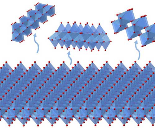
Serving up fresh, clean, and monolayer-thin MoO3 nanosheets(Nanowerk News) The 2010 Nobel Prize in physics was awarded to Manchester scientists Andre Geim and Konstantin Novoselov for their pioneering work with graphene, a 1-atom-thick, two-dimensional (2D) network of carbon that may revolutionize computing and electronics. Molybdenum trioxide (α-MoO3) also contains such 2D layers, which are linked together through weak van der Waals forces that cause a molecule to become attracted or pushed away from another molecule. |
|
| The unique layered-structure makes α-MoO3 an attractive material for use in lithium ion batteries and electrochromic devices, such as „smart” windows that control solar light absorption in buildings and auto-dim rearview mirrors that protect drivers from high-beam lights. | |
 3 molecular fragments from the surface of a single monolayer during film growth” border=”0″ align=”middle”> |
|
| Schematic representation of the re-evaporation of α-MoO3 molecular fragments from the surface of a single monolayer during film growth. At the optimum substrate temperature, only one monolayer “sticks” to the substrate because of strong interaction between the two; all other monolayers desorb because of weak van der Waals interaction with the first layer. | |
| Results | |
| Materials scientists at Pacific Northwest National Laboratory have overcome a set of challenges in synthesis and isolation of ultra-thin α-MoO3 layers. They developed a reproducible method for growing α-MoO3 sheets down to a monolayer in thickness. They used a thin-film deposition technique, molecular beam epitaxy (MBE), to synthesize α-MoO3. A stable oxide substrate provided the needed template (Nanoscale, „Iso-oriented Monolayer α-MoO3(010) Films Epitaxially Grown on SrTiO3(001)”). | |
| The secret to growing monolayer-thin α-MoO3 is multi-faceted. The scientists’ success hinged on the right substrate that provides lateral confinement to the α-MoO3, and the carefully identified growth temperature, which allows α-MoO3 seeds to evolve, grow, but stop right at the monolayer thickness. Their results, which can greatly advance our current understanding on the material’s physical and chemical properties, appear in the scientific journal Nanoscale. | |
| Why It Matters | |
| Besides electrochemical and catalytic applications, ultra-thin α-MoO3 has also demonstrated its potential use in thin-film pseudocapacitors, light-emitting diodes, plasmon resonance generators, and biosensors. It is critical to be able to synthesis and isolate such 2D materials in a contamination-free environment (ultra-high vacuum) to better understand their intrinsic properties. The PNNL science team was able to meet these high standards by combining instrumentation and capabilities in the Environmental Molecular Sciences Laboratory (EMSL), a DOE national user facility. | |
| Methods | |
| „To grow the layers, we evaporate high-purity MoO3 powders held in a ceramic cup in ultra-high vacuum and put a substrate in front to collect the molecules,” said Dr. Yingge Du, lead scientist on the project. The evaporated MoO3 molecules will condense and form a well-ordered thin film on the heated substrate. | |
| Du likens the substrate to a Lego© base plate. „If you throw atoms together randomly, they will stick together like a pile of Lego pieces in a random, messy way. But with a good base template, you can position the Legos in an ordered fashion, and make nice structures.” | |
| And, MoO3 film growth is temperature sensitive. „At lower substrate temperatures, the material will grow as amorphous layers and become thicker and thicker. At higher temperatures, unwanted phases and structures start to evolve,” Du said. „We were extremely delighted that a very narrow temperature window was found for us to grow this material as a single monolayer.” | |
| The correct temperature-in this case, 450°C-allows a crystalline layer to form on the substrate, stabilized by interfacial chemistry. However, the growth of subsequent MoO3 layers is suppressed by material re-evaporation from the substrate. The high substrate temperature and weak van der Waals bonding between adjacent MoO3 layers allow a self-limiting growth process, which provides a highly reliable technique for MoO3 to form and stay as a monolayer. | |
| „Using traditional methods, these nanomaterials are hard to grow or isolate. The trick is to find the optimal temperature that not only provides enough thermal energy to start the crystal structure, but also is high enough to de-adsorb additional layers,” said Du. | |
| What’s Next? | |
| The research also paves the way to creating phase-pure, thicker films by lowering the growth temperature once the monolayer template is formed. The team plans to further investigate the electronic, transport, and catalytic properties of these films using various in situ spectroscopy and microscopy techniques at EMSL. |
| Source: Pacific Northwest National Laboratory | |
Read more: Serving up fresh, clean, and monolayer-thin MoO3 nanosheets
O piele inteligentă auto-alimentată, ca cea recent dezvoltată de o echipă de cercetători chinezi, rezolvă fundamental această problemă. În această lucrare, oamenii de știință combină efectul triboelectric și inducția electrostatică plană și o aplică într-o structură subtilă pentru prima dată pentru a crea o piele inteligentă analogică inteligentă.
Posted: Apr 08, 2016
(Nanowerk Spotlight) In order to make robots and robotic technology more human-like and more human-friendly, smart skin technology is a critical element that helps robots sense the world. These electronic or smart skins could help machines to accurately perceive the environment and better assist human owners.However, conventional smart skins – no matter if they are based on resistance, capacitance or transistors – all need a power supply. It’s kind of awkward for users to have a high-tech, state-of-the-art thin, flexible and light-weight smart skin and have to power it with a hard and heavy battery which can just work for hours.Furthermore, in conventional smart skins higher resolution always means higher energy consumption and complex circuits. These two aspects need to be carefully balanced to result in a practical device. So the obvious question is: Is it possible to achieve higher resolution and at the same time reduce energy consumption?A self-powered smart skin as the one just recently developed by a team of Chinese researchers fundamentally solves this problem. In this work, the scientists combine the triboelectric effect and planar electrostatic induction and apply it in a subtle device structure for the first time to create a self-powered analogue smart skin. Structure of analogue smart skins. (a) Schematic diagram of an analogue smart skin. (b) Optical image of the transparent, flexible, and lightweight smart skin. The smart skin with a honey bee landing on it will not deform the peony. (c) SEM image of microstructures on the PDMS film. (d) SEM image of the silver nanowire electrodes. (Reprinted with permission by American Chemical Society)Reporting their findings in ACS Nano („Self-Powered Analogue Smart Skin”), a team led by Prof. Haixia Zhang at the National Key Laboratory of Science and Technology on Micro/Nano Fabrication, Peking University, presents a self-powered analogue smart skin to detect location as well as contact velocity, based on a single-electrode contact electrification effect and planar electrostatic induction.In this paper, the team presents two significant achievements. The first is that their smart skin is intrinsically self-powered.”We use spontaneous triboelectric charges, combined with planar electrostatic induction, to sense the touch applied on the smart skin,” Zhang explains to Nanowerk. „Triboelectric charges occur in our daily life everywhere when two surfaces touch each other. And when the charged surface approaches a metal block (or electrode) it will induce the opposite charge, which is the so-called ‘electrostatic induction’ effect.”The beauty of this approach is that it makes use of the charges from triboelectric effect – which exist everywhere. Imagine a scenario, when you want to drink some coffee: you walk towards a table, and by doing so the opposite charges will be generated on the surface of shoes and ground respectively; you pick up the cup to drink, and the opposite charges will be generated on the skin of your palm and the handle of the cup; furthermore, even swallowing the coffee will generate charges on the surface of your digestive tract and the coffee.The Chinese researchers utilize these spontaneous – but often be ignored – charges to make their smart skin completely self-powered.The intensity of the electrostatic induction effect depends on the distance between the charged surface and the metal electrode. The scientists use fixed electrodes to detect the intensity of the electrostatic induction effect, allowing them to confirm the location based on the relative intensity.That way, no extra power supply is required for operating the analogue smart skin.The second achievement is that only four electrodes are necessary to achieve millimeter bi-dimensional resolution (precision) because of the utilization of analogue localizing method to sense the touch stimulation.”Compared with the previous works (see references 1-3 below), this smart skin reduces the number of electrodes remarkably,” Zhang points out. „This helps a lot to reduce the complexity of the signal processing circuit. Although using less electrodes, our smart skins achieve 1.9 mm resolution, much better than previous results.”She notes that, compared with digital smart skins which have been studied extensively, analogue smart skins still need more in-depth study.”Analogue smart skins have obviously advantages at resolution and energy consumption,” she says. „I hope our work can draw more attention to the field of analogue smart skins. Furthermore, it will contribute to the areas of artificial intelligence and portable electronics as the self-powered high-resolution sensor offers a solution for smart skin applications.”
 Use of smart skin on an artificial hand. (a) Photograph of an artificial hand covered by two-dimensional analogue smart skins on the curved back of the hand and one-dimensional analogue smart skins on the middle finger. (b) Voltage output when a honey bee approaches and leaves the two-dimensional smart skin swiftly. (c,d) Voltage ratios of electrodes a-d. (e) Voltage output when the two-dimensional smart skin on the artificial hand is touched. (f) Location result of analogue smart skins. The testing point is (2.50, 2.50), and the result is (2.53, 2.50), with a slight deviation of only 0.3 mm. (Reprinted with permission by American Chemical Society) (click on image to enlarge)Going forward, the team will work on the stretchability of their smart skin (the current version is not stretchable) and on improving the resolution. According to the team, due to the theoretically infinite resolution, there still is plenty of room to improve on the current performance. Furthermore, they will try to integrate more sensing parameters as well as signal transmission in the design.Last but not the least, they will explore approaches to shield the smart skin from environmental interference, which is critical for practical applications.Zhang notes that the current device design provides opportunities for including additional sensing capabilities such as temperature, contact velocity, or gas composition.References1) Takao Someya’s Group,36 electrodes for 64 square centimeter smart skins. Kaltenbrunner, M, et al. „An ultra-lightweight design for imperceptible plastic electronics.” Nature 499.499(2013):458-63.2) Zhenan Bao‘s Group, 16 electrodes for 4 square centimeter smart skins. Lipomi, Darren J., et al. „Skin-like pressure and strain sensors based on transparent elastic films of carbon nanotubes.” Nature Nanotechnology 6.12(2011):788-792.3) Do Hwan Kim’s Group, 14 electrodes for 16 square centimeter smart skins. Kim, So Young, et al. „Highly Sensitive and Multimodal All-Carbon Skin Sensors Capable of Simultaneously Detecting Tactile and Biological Stimuli.” Advanced Materials 27.28(2015):4178-4185.By Michael Berger – Michael is author of two books by the Royal Society of Chemistry: Nano-Society: Pushing the Boundaries of Technology and Nanotechnology: The Future is Tiny. Copyright © Nanowerk
Read more: An analogue smart skin that is self-powered