
Masca de gaze (filtru NCB , M95,CB,C4,NA 50)
Filtru cartus NCB 40 mm, tipuri si preturi
Cea mai usoara masca de protectie C4
Masca M95- descriere si accesorii
Masca de gaze CB , cu protectie excelenta si camp de vizibilitate mare
Filtru NCB 2200
Filtru cartus NCB 40 mm, tipuri si preturi
Cea mai usoara masca de protectie C4
Masca M95- descriere si accesorii
Masca de gaze CB , cu protectie excelenta si camp de vizibilitate mare
Filtru NCB 2200
Polimerii noi sintetici arată promisiunea pentru crearea de medicamente rezistente la mediul înconjurător, care nu pierd potență în timp
Composite balistice ușoare;
CO2 capturat fie direct din atmosferă, fie dintr-o centrală de gaze naturale cu ciclu combinat, poate fi electrolizat pentru a produce gaz de oxigen și nanofibre de carbon, care pot fi apoi folosite pentru a produce o varietate de produse valoroase
O echipă de cercetători de la Academia Chineză de Științe și Universitatea din California a găsit o modalitate de a degrada plasticul obișnuit într-un mod care să permită crearea unui combustibil din gunoi de plastic.În plus, catalizatorii sunt compatibili cu diferiți aditivi de poliolefine
cele mai recente cercetări relevă de ce geckos sunt cele mai mari animale capabile să scadă zidurile verticale netede – chiar și alpiniștii mai mari ar necesita picioarele lipsite de manevră mari;iar scalarea este esențială pentru îmbunătățirea performanțelor adezivilor pe suprafețe mult mai mari
Informații privind peisajul dezvoltării senzorilor;cresterea comunicatiei;Workshop pentru nanotehnologia senzorilor
Avionul Hipersonic Atac (HAA) / „Nuke Glider” și Yu-74 Ultra-Maneuverable Hipersonic Glide Vehicule (HGV)
Dezvoltarea fotodetectoarelor a fost o chestiune de interes considerabil în ultimele decenii, deoarece aplicațiile lor sunt esențiale pentru multe domenii diferite, cum ar fi camerele, dispozitivele medicale, echipamentele de siguranță, dispozitivele de comunicații optice sau chiar instrumentele de măsurare, printre altele.
| Posted: Jun 17, 2016 | |
A new form of hybrid photodetectors with quantum dots and graphene(Nanowerk News) The development of photodetectors has been a matter of considerable interest in the past decades since their applications are essential to many different fields including cameras, medical devices, safety equipment, optical communication devices or even surveying instruments, among others. |
|
| Many efforts have been focused towards optoelectronic research in trying to create low cost photodetectors with high sensitivity, high quantum efficiency, high gain and fast photoresponse. This is of paramount importance especially in the short wave infrared which currently is addressed by very expensive III-V InGaAs photodetectors. The development of two main classes of photodetectors, photodiodes and phototransistors, have partially been able to accomplish these goals because even though they both have many outstanding properties, none seem to fulfill all of these requirements. While photodiodes are much faster than phototransistors, phototransistors have a higher gain and do not require low noise preamplifiers for their use. | |
| To overcome these limitations, ICFO researchers Ivan Nikitskiy, Stijn Goossens, Dominik Kufer, Tania Lasanta, Gabriele Navickaite, led by ICREA professors at ICFO Frank Koppens and Gerasimos Konstantatos, have been able to develop a hybrid photodetector capable of attaining concomitantly better performance features in terms of speed, quantum efficiency and linear dynamic range, operating not only in the visible but also in the near infrared (NIR: 700-1400nm) and SWIR range (1400-3000nm). | |
| At the same time this technology is based upon materials that can be monolithically integrated with Si CMOS electronics as well as flexible electronic platforms. The results of this work have been recently published in Nature Communications („Integrating an electrically active colloidal quantum dot photodiode with a graphene phototransistor”). | |
 |
|
| This is a schematic of the device structure. (Image: ICFO) | |
| To be able to achieve this, the team of researchers developed a hybrid device by integrating an active colloidal quantum dot photodiode with a graphene phototransistor. By including an „active” quantum dot photodiode, they were able to increase charge collection in a highly absorbing thick QD film, which in turn increased the quantum efficiency as well as the photoresponse. The active quantum dot layer enabled a more effective charge collection by exploiting carrier drift towards the graphene layer instead of relying only on diffusion. The researchers then combined this scheme with a graphene transistor to register ultra-high-gains and record gain-bandwidth products, thanks to Graphene’s 2D character and remarkably high carrier mobility. | |
| The results obtained in this study have shown that this hybrid architecture does clearly demonstrate the potential of graphene and active quantum dot materials, opening new pathways for their integration in other optoelectronic materials in search for much higher performance and a broader spectrum of functionalities. |
| Source: ICFO |
Un material semiconductor nou, care are doar trei straturi atomice groase, a apărut cu proprietăți electronice mai exotice, maleabile decât cele ale semiconductorilor tradiționali.Un nou material semiconductor ultra-subțire (disulfură de wolfram sau WS 2 ) constă din trei straturi atomice într-o configurație „sandwich atomică”, cu un strat de atomi de tungsten de metal greu între straturile de atomi de sulf mai ușori. Materialul este cvasi-dimensional, are doar trei atomi grosime și prezintă o structură electronică unică, cu diferențe subtile, în funcție de direcția în raport cu legăturile atomice repetate în planul stratului.
| Posted: Jun 17, 2016 | |
Laser manipulates electronic properties(Nanowerk News) A new semiconducting material that is only three atomic-layers thick has emerged with more exotic, malleable electronic properties than those of traditional semiconductors. These properties come from electrons, like a ball rolling down a hill to a valley, that prefer the lower energy levels at the bottom of electronic energy “valleys”. Now, the valley depth can be shifted optically and with extreme speed with sculpted laser pulses (Nature Materials, „Valley-selective optical Stark effect in monolayer WS2„). |
|
 |
|
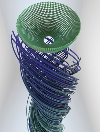
| Electrons have distinct energy levels where the energy is minimized, similar to a ball rolling down a mountain to a valley. In the artistically enhanced depiction, a valley in the electronic structure interacts with and is controllably manipulated by circularly polarized laser light. The laser causes valleys with initially equal energies to have slightly different energies. This is the first time a laser has separated energy valleys in an atomically thin semiconductor (tungsten disulfide), which could lead to advanced electronics based on energy valley states instead of conventional electronics based on charge flows and accumulation. (Image: Massachusetts Institute of Technology. Illustration by Ella Marushchenko and Alex Tokarev) | |
| Layered materials where electrons are constrained to two dimensions can be engineered into novel electronic structures with unique electronic and optical properties. Optical manipulation of electrons can lead to new modes of energy conversion and computational devices such as electronics based on energy valleys states instead of conventional electronics based on charge flows and accumulation. | |
| A new ultra-thin semiconducting material (tungsten disulfide or WS2) consists of three atomic layers in an “atomic sandwich” configuration with a heavy metal tungsten atom layer between lighter element sulfur atom layers. The material is quasi-two dimensional, just three atoms thick, and exhibits a unique electronic structure with subtle differences depending on the direction relative to the repeating atomic bonds in the layer plane. | |
| The differences create two distinct but similar valleys in the electronic structure, where electrons can accumulate with different directions, but with associated energy levels and gaps that are equal. Adding a specific type of laser beam, where the polarization direction (the direction of interacting electric forces) rotates as the light propagates, creates a new type of electron energy structure that can be probed and manipulated. | |
| The electron structural landscape, which began with two similar valleys, can also be made to have different distinct valleys with different energy depths. The valley depth can now be manipulated with light to encode information like zeroes and ones for conventional data. | |
| Additionally, changing the energy of the valleys with light allows for fast manipulation without the need for contact with complex electrodes as in conventional electronics. |
| Source: Department of Energy, Office of Science |
Armura corpului include o primă placă blindată având o suprafață posterioară concavă, o a doua placă având o suprafață frontală convexă și, opțional, un strat separat de cuplare configurat să se potrivească între prima placă de armă ceramică și placa de polimer